POLY-SS MICROCOMPUTER SYSTEM
VOLUME I: ASSEMBLY, TEST, AND THEORY OF HARDWARE
©
1976 IPCPOLYMORPHIC SYSTEMS
737 South Kellogg AvenuePLEASE NOTE
Several erratta sheets are included
at the end of this manual. Be sure
to read the erratta pertaining to
TABLE OF CONTENTS
A. Assembly and Test . . . .
1. Check all components for inclusion . . . .
a. Backplane, cabinet and power supply . . . .
1
1
1
b. Proces sor b o a r d . . . 3
c. Video board . . . 5
2. Assemble cabinet, backplane and power supply . . . 8
a. Assemble backplane . . . 8
b. Assemble chassis . . . 9
c. Test backplane and power supply . . . 13
3. Assemble processor board . . . 14
a. Install voltage regulators . . . 14
b. Install integrated circuits . . . 15
c. Install discrete components . . . 16
4. Assemble video board . . . 19
a. Smoke test . . . 22
b. Install integrated circuits . . . 22
c. Option selection . . . 23
d. Select character line length option . . . 24
e. Address location . . . 24
f. Interface TV monitor or receiver . . . 25
g. Connect keyboard . . . 26
h. Keypress strobe . . . 27
i. Optional volatge regulator . . . • . . . 28
5. System checkout . . . : . . . 28
a. Video board checklist . . . 29
b. Central processor checkout . . . 43
B. Theory of Operation . . . • . . . 45
1. Video Terminal Interface . . . 45
a. Block diagram . . . 46
b. Schematic diagram . . . 46
2. Central processing unit . . . 52
a. Block diagram . . . 52
b. Schematic diagram . . . 53 Appendix
A. Schematic foldouts
PolyMorphic Systems POLY 88, Vol. I Rev.O.O P. 1
POLY 88 Microcomputer System Manual
VOLUME I: Assembly, Test, and Theory of Hardware
This volume explains hm·, ·to assemble and test the POLY 88, a complete microcomputer system that interfaces with an ASCII
keyboard and video monitor. It also explains how the hardware
works. Volume II discusses system software, and offers hands-on
experience with the system.
The assembly and test portion of this volume is intended for those
who have unassembled kits. If your POLY 88 is assembled, turn
directly to Section A.5, system checkout. That section concerns
inserting assembled circuit cards into the chassis' and checking
for correct operation. Those with assembled systems will find
the remainder df this volume interesting mainly as a source of reference.
A. Assembly and Test
1. Check all components for inclusion.
The POLY 88 microcomputer system in unassembled form consists of three packages containing the components for the three
sub-assemblies, plus a two-volume manual. The three sub-assemblies
are:
a. backplane, cabinet, and power supply.
b. central processor sub-assembly.
c. video terminal interface.
Following are complete parts lists. Check each sub-assembly for
inclusion of all components. If any component is missing, see
the enclosed warranty.
PolyMorphic Systems POLY 88, Vol. I Rev. 0.0
Backplane and power supply components are packed inside the cabinet. Lift off the cabinet and verify that packed inside it are:
check
(~'
ba.ckplane circuit board(v1'
two boxes of componentsP. 2
The cube-shaped box contains the transformer. The other box contains all the miscellaneous components for the backplane and power supply. They are:
check
(1--t
(~('B
(-\)(~
~~
(I)'
~<o(v(, (0'(c/)
(11'5
(0
(0
(/)
{vi'
1 1 i ne cord
1 17,000
pF
capacitor (15V) 1 2,00npF
capacitor (SOV) 1 1,000pF
capacitor (SOV)2 100-pin edge connectors
1 lighted reset b~tton
1 lighted power s.Jitch 1 fuseholder with hex nut
Z 'plastic slotted card guides 1 strain relief
'.1 3-Tug te·rminal ·strip 2 6-amp power diodes 4 l-amppower diodes I 330-ohm ~ W resistor
(60S0S) (IN4003)
1 0.1
pF
ceramic disc capacitor 2 IOO-ohm ~ W resistb~s2 2200-ohm ~ W resistors
(0
( 0/) 1 1000-ohm ~ W resistor
470-ohm \ W'resistor 2N5449 transistor 1N4148 diode
(/5,
1(.1
1(0'
1(V) 6 hex~gonal metal standoffs
@16V
PolyMorphic Systems. POLY 88, Vol. I Rev. 0.0
{v5
2 Card guide brackets (one front and one back)10-32 screws, lockwashers, and nuts
(t--t"
4(~ 24 6-32 X ~" screws
4
6-32X
~ screws~.
8 6-32 nuts and stan-lashers
4 rubber feet
P. 3'
(U'
~+ () 2~'-2
flat plastic insulators (or plastic backing on brackets) pairs of Molex connectors with assorted pins
(~~
(L.-}.-r 1
(vr
8(vY'
1(//j (v)
( )
Green, orange, and blue wire (26") length of shrink tubing
small forked standoffs
2 Amp fuse
solder
black wire (6")
Additional edge connectors, if ordered, plus additional
4-40 screws, nuts, and fiber washers, are also in this box.
b. Processor board
Processor and video board components are packed in the remaining
two boxes. The processor board box contains clear plastic bags.
One bag contains the processor circuit board. Th~ others, numbered
starting with
0,
contain the components to be mounted on theboard. Check each bag to see if an components are included.
BAG
0:
INTEGRATED C.IRCUITS (38 in all)check
( n l C 808 0 Ace n t r a 1 pro c e s sin gun i t
(iY1
1 8224 clock generator( ) 1 C2708 Monitor read-only memory
('1
4 M191l11APC 256 X 4 random-access memories (or type 2111 1s)(vj"'6 N8T97B bus drivers
(~3 74LSI09
(0
2 74LS138(v)"
2
74lS174(v-r"2
74LS257PolyMorphic Sys terns POLY 88, Va 1 . I Rev.
(y/
1 74LS08(-1' .... , 1 74LS132
(0'/ 1 7425
(0
1 7407(v-f' 1 74148
(vJ
1 74LSOO(?) 1 74LS02
/
(v) 1 74LS04
(vf 1 74LS13
(v(
1 40 pin socket(vf
3 24 pin socketBAG #1: HARDWARE
CHECK
(Yj/ 2 6107B-14 Thermalloy heatsinks
U-"(
1 6051B Thermal1ay heatsink(,~ ) mica insulator
(v('"
3 6-32 X 3/8" screws(0
3 #6 star washers(v,.r'" 4 6 -32 hex nu ts
(0
1 #6 fiber washer(v"r ",1 6-32 X 3/811 nylon screw
(v)"" 1 LM309K or U4340K-5.0
(~ 1 MC78M12PC
(~'1 MC79M05PC
0.0 P. 4
BAG #2: DISCRETE COMPONENTS
CHEC K
{ V(,
2II
2, 2 00 -0 h m res i s tor s(II"(
.3
1,000-ohm resistors(0'
(v)'
('-1"
(0'
1 4,700-ohm resistor
8 10,000-ohm resistors
1 470 pF ceramic disc capacitor
PolyMorphic Systems POLY BB, Vol. I
(vy
1 33 JlF tantalum capacitor(~~ 1 39 pF ceramic disc capacitor
(Yf"-
31 0.1 JlF ceramic disc capacitors(.f-
2 IN414B diodes(t"r
1 16. 5BBB HHZ crys ta 1(~ 5" teflon sleeving
(~" 6" bare wire
Rev. 0.0
The following bags contain components for options that mayor may not have been ordered.
BAG #3: SOCKET KIT
check
(~ 4 lB-pin sockets
(vj-17 16-pin sockets
(vj"12 14-pin sockets
BAG #4: RECEIVER/TRANSMITTER PACKAGE
"
( 0 . 1
~1i~5307
programmable baud-rate generatorsr
(t.1/ 1 B251 universal synchronous/asynchronous receiver/
transmitter with socket
(1/( 1 74LS08
(V),- 2 14 pin sockets
( V(
1 IN4148 diode{j/(d 1 79L12 regulator
(v]
_1
10 JlF tantalum capacitor(v('
2 .1 JlF ceramic disc capacitorsc. Vi d eo bo a r/d
P. 5
The last box contains bags of components for the video terminal
interface. One unnumbered bag contains the circuit board. Check
PolyMorphic Systems POLY 88', Vol. I Rev. 1.2 P .
BAG #0: INTERGRATED CIRCUITS
check
{n
1 SN7407N(~
2 SN74150N{ 3 SN74367N or DM8097N
(0"
2 SN74393N( t--1-"
2 SN74LSOON(~ 1 SN74LS02N
(vr-
1 SN74LS20N(~. 2 SN74LS74N
(W' 1 SN74LS123N
( vY':-
2 SN74LS132NUf~
1 SN74LS138N1 SN74LS139N
(W' 1 SN74LS153N
(~- 5 SN74LS157N
(J...y- 3 SN74LS161N
(~ 1 SN74LS273N
(~ 1 SN74S124N
(p.-f' 1 SN74S412N or P8212
(~ 1 MCM6571A or MCM6574 or MCM6576
(*.
4 AM91LllAPC [);Z Ii I.tl 1..-1/~~.
1 DM8131N1 N82 74 B
BAG #1 : DISCRETE COMPONENTS
check
(v). 1 Capacitor-Silver Mica 22pf @ 150v CD15ED220J03
(v-('
1 Capacitor-Silver Mica 39pf @ 150v CD15ED390K03(~.' 6 Capacitor Tantalum lOmf@25vT362B106M025AS(Kemet)
(v~ .. 1 100pf
2:.
10% Ceramic Disc(VI 1 Capacitor Ceramic .0047 @ 25v
·{~-~~~tor G~m+e--4-~
(~_ 1 Regulator lM323K
(Y'J/ 1 MC78Ll2CP
(~ 2 Trimpot 10K ohm 72WR10K
(YJ. 1 Resistor 820hm ~w
(~ 1 Resistor 100 ohm ~w
(~ 2 Resistor 220 ohm ~w
tv[ .,
1 Res i s tor 4 70 0 h m ~w(~- 4 Resistor 1000 ohm ~w
(....;. 1 Resistor 3300 ohm ~w 10%
(vr:::
2 Resi stor 4700 ohm ~w(~ 1 Transistor 2N5449
~.---.---'-'---~
(0 I D BAG #2: HARDWARE, ETC.
check ( )
(
)
()
( )
30 Capacitor Ceramic .lmf @ 16v UK16-104
1 Heat sink 6051
14 Resistor 2200 ohm~w
1 Bag Hardware
PolyMorphic Systems POLY 88', Vol. I Rev. 1.2
VIDEO HARDWARE (SHIPPED IN BAG #2) check
( )
( ) ( ) ( ) ( ) ( ) check2 6-32 X 3/8 11 pan head screws
2 #6 Hex nut (small pattern) 2 #6 Lockwasher
1 1211 #24 bare wire 1 611 Teflon sleeving 1 15 feet solder
BAG #3: MEMORY OPTION
( ) 4 Capacitor Ceramic .1mf @ 16v
( ) 4 AM91L11APC
BAG #4: SOCKET SET
check
(vt· 2 Male Receptacle 22-05-2021
(~ 1 Female Connector 08-50-0114
(0- 1 Plug Housing Molex 22-01-2021
(J..--}- 11 Socket-14 pin Low Profile
(H-
18 Socket-16 pin Low Profile(~ 8 Socket-18 pin Low Profile
(vJ· 1 Socket-20 pi n Low Profi 1 e
(v-r
4 Soc k e t - 2 4 pin Low Pro f i 1 e(t--t-
1 14 pin sidew;ping(v}
1 CTS20607 14 pin Dip Slide Switch(t.-1--····1 Coaxial Cable) 1 Foot
check ( ) ( ) ( ) ( ) ( ) ( ) ( ) ( ) ( ) check
BAG #5: POLY 88 ACCESSORIES
2 MALE PC RECEPTACLE 22-05-2021 1 FEMALE CONNECTOR 08-50-0114
1 HARDWARE FOR AMP 206584-1, 205817-1 1 CONNECTOR AMP 206584-1
1 REAR MTG PHONO PLUG
1 RIBBON CABLE 3M 06/06/65-15 1 PC BOARD-PARALLEL
1 BAG HARDWARE
COAXIAL CABLE 1 FOOT
SUPPLEMENTAL HARDWARE (SHIPPED IN BAG #5)
) 2 4.40 X 3/8 11 Pan Head 'Screws
) 2 2.40 Hex nuts
) 2 #4 Star Washers
) 1 6.32 X 3/8 11 Pan Head Screws
) 1 6.32 Hex nuts
) 1 #6 Star Washers
) 1 1" shrink tubing
PolyMorphic Systems POL Y' 88 t Vol. IRe v. O. 0 P.8
2. Assemble cabinett backplane, arid power supply
The first step in building the POLY 88 is assembling the back-plane, starting with the discrete electronic components
(small-est through larg(small-est), then card guides t then sockets. The
transformer is then assembled into the chassis, and the backplane mounted and connected.
a. Assemble backplane. Refer to figure A-l to see where the
components go on the board. When installing discrete components,
solder on the back of the board and trim leads.
(J
1. Install standoffs for four 1-amp power·diodes, with forksup. (for 03 through Ofi -- see fig. A-I.) Clip off extra pin b;low board.
NOTE: The extra holes with diode symbol nearest the center are not used.
(~.
Install IAdjo~es
(lN4003) onto standoffs (03 through,06)oriented as indica~ed by the arrow on the' board. The banded
end of the diode points in the direction th~e arrow is pointing.
(v)
3. Install both 6-amp power diodes in place (01-02). Thesetwo diodes alone provide full-wave rectification with the center-ta pped trans former. (60505)
(~4.
Install two~,200-ohm
resistors RI and R2.(~ 5. Install the 330-ohm ~ Wresistor R3.
(v1"
6. Install one lOa-ohm ~ W resistor R4.(0'7. Install the other laO-ohm ~W resistor R5.
(M8. Install the lN4148 diode 07.
(red-red-red)
(orange-o range-brown) , (brn-blk-brn)
(~9.
Install the ceramic disc capacitor C4. ( .1 ,uF)(V}lO. Install the 1,000-ohm resistor R6 at the other end of the
board. (brn-bl k-red)
(vrl1.:.Instal1 the 470-ohm r.esistor R7. . (ylw-viol-brn)
(vf),2.' Install the 2N5449 transistor Ql oriented as shown.
(yf'13 .. Install the 1,000 J.1F electrolytic capacitor C2 .
PolyMorphic Systems . POLY 88, Vol. I Rev. 0.0 p .9
.
( 0"
1 4 . Ins tall the 2, 000 f.4 F e 1 e c t r 0 1 Y tic cap a cit 0 r CItoriented with its positive end in the direction indicated on the
boa rd.
(v1
15. Using the screws supplied on the capacitors, attachthe 17,000 JlF electrolytic capacitor C3. (Noting the polarity)
(/1""'16. Attach plastic card guides to metal card-guide
supports, using 6-32 screws and nuts. (Nuts on inside.)
(v)
17. Mount card guides as shown. Use short 6-32 screws andsix metal standoffs. These are protected from the circuit board
by p 1 a s tic ins u 1 a to r s •
(I/}
18 . . Attach two 100-pin edge connectors (or up to five asdesired) into connector areas J1 and J5 as shown. Making sure
that the connector does not bow the backplane, solder all 100
pins on each connector. Be careful not make solder bridges.
(~19.
Solder male halves of Molex connectors into each end of board as shown on page 10.?
(...1
20. Install a wire jumper on front of board as shown. (R8)-Ii
The backplane is now complete.
b. Assemble chassis.
Do not solder until instructed to do so.
(V('.
1.4 #6-32
(v(
2.Install 4 rubber feet to chassis undersides, using x 3/8 screws, nuts, and lockwashers.
Install fuseholder on rear of chassis, with perpendicular tab pointing down.
(Vf 3. Tin the 1 ine cord wires and trim the exposed ends to abou~
3/811 •
(~
4. Install through rear of chassis using the strain reliefprovided, allowing about 2 inches of the heavy outside insulatio~
inside beyond the strain relief. Pliers or a strain relief tool
wi 1 1.. be n e c e s s a r y, due to the t i 9 ht fit.
(~5.
Attach the black wire from the 1 ine cord to the end of the fuseholder and solder in place.(0
6. Take the transformer and cut the secondary wires (yellow,PolyMorphic Systems POLY 88, Vol. I Rev. 0.0 P.10
orange }
orange
redlwhite open end yellow
yellow-- closed end
«()
7. Attach and solder the 5 larger mol ex pi ns to secondary wires, making sure the one with the closed tip goes on oneof the yellow wires, and the red and white wires are together on one pin. Use needle pliers to crimp pins and solder to insure good connections.
(v('
8. Insert molex pins in the connector as shown~bove.
(y('
9. Cut the blue and black primary wires down to 5 inchesand the red and brown wires to 8~ inches, strip to about 3/8
inch, and tin.
(
~1
0 . The rem a i n i n g 2 w ire s ( g r e en, 9 ray) m us t be k e p t fro m shorting to anything else. Cut one of these wires to about 3 inches and the other to 2 3/4 inches, place a 1 inch length of shrink tubing on the two wires so that ~ inch extends pastthe end of the longer wire. Shrink the tubing by using a match; pinch the end of the warm tubing to seal the wire inside.
CAUTION: Do not burn the tubing by allowing the flame to touch it_
(v)
11 _ Ins tall roc k e r power s w i tc h i n fro n t 0 f c has sis wit hthe 2 closer contacts at the top.
{~12.
Take the 3 20 inch lengths of wire, strip to about 3/8 inch and tin (both ends). Then twist the 3 wires together, leaving l~ inch loose at each end.U·{
13. Attach a nd so lder these 3 wi res to the power swi tch from the bottom up. The order should be green-bottom, orange middle, and blue-top_(") 14.
Take the 3 lug terminal strip and attach green wire from line cord to the grounded lug on terminal strip and the 'i/hite wire to another lug. To make later connections to@"
n,,"
uf~
'0
FIGURE At
1
0
I·'
1
0
I··
;;1~
~ ')f~'+
N{),,'IIEY
ST.4Nb/)fF~/#~'"
6 places,
V
V
NUT AlO, 4{f x)
WAShiER ttJCK ,v04(f%)
WA5#,Eh' Fl8ENNtJ.l.(fK)
c. PLACES
per connector'
SCREW 6-3c X . .?S' LG.(jX)
3Pf.ACE5
NUT NO 6 rex)
4flACE5
WA5HER INTERNAL 5MR LOt/( (eX)
VENDOR 5UPPLIED SCREW 4-40X .(,2 L 6
(5X;-2 PLACES
per connector
4 PlACES
SCREW 6-3CX .38 LG(t?tV
PolyMorphic Systems POLY 88, ~ol. I Rev. 0.0 P.ll
w~ires in place now. This terminal strip will be attached to the
foot f the transformer as shown on the next page.
( 1 5 . Attach 1 of the .01 IlF disc capacitors from the side lug of the fuseholder to the terminal strip lug with the green wire attached.
(0'
16., Attach the blue wire from the power switch on the front of the chassis to the side lug on the fuseholder, and solder at th i s poi n t. .(~17.
Attach the green wire from the power switch to the same terminal strip lug·to which you already attached the white line cord wire.(?i8. Attach and solder the remaining .01 IlF capacitor between the lug used in step 17 and the grounded lug of the terminal strip and solder the lug with the two caps.
(Wt9. Placing the transformer beside the chassis, but without yet installing it, attach its blue and black primary wires to the
te~ lug with the white line cord wire and solder.
{yj 20. Take the transformer and turn it so the secondary wires are on the Same side as the terminal strip and attach it into place in the rear of chassis, being very caieful not to pinch any wires under it. The terminal strip should be installed on one foot of the transformer above the fuseholder.
(v)
21. Attach the orange wire from the power swi tch and rema i n-ing red and brown primary wires from the transformer to theremaining empty lug on the terminal strip and solder. These are ~he only connections to this lug.
(~,22.
Solder all connections to the terminal strip now.(v{23. Take the 4~ inch long wires (orange, black, green,
blue), strip and tin both ends to about 3/8 inch, and crimp the 4 smaller molex pins to one end. Solder again to insure
goo~ connecfjons. '
{v(
24. Trim~ff
about haif center of the reset button. to the button as shown:~
PolyMorphic Systems POLY 88, Vol. I Rev. 0.0 P.12
green
-"'1'
'I_blue
~~-_'
__
'_~~I
black orange(I>
25. Insert molex pins into the small female molex connector as shown:orange
green
bl e black
( r('
2 6 . Ins e r t con n e c to r t h r 0 ugh s qua r e h ole 0 n fro n t pan e 1and draw the wires through. With the green and blue wires at the top, snap the switch firmly in place.
u/f
27. Assemble backplane into chassis by sliding the endwith the two horizontal filter capacitors under the transformer, align the hexagonal standoffs with the six holes in the bottom of the chassis. Fasten the backp~ane in place with six #6-32 screws, making sure not to pinch the wires running to the power switch.
(v)
28. Connect the backplane to the transformer and the reset switch by mating themolex connector at each end of thebackplane.
PolyMorphic Systems POLY 88, Vol. I Rev. 0.0
c. Test backplane and power supply.
If you have a small voltemeter, you can now check the backplane and power supply. Plug in the-chassis and
P • 1 3
II s m 0 k e t est II it. I f any t h i n g i sob v i 0 u sly w ron g, don' t
go any further till you've eliminated the problem.
Next, turn the cabinet so that the transformer is on your left. Along the edge of the backplane circuit board nearest you is a row of finger~like pads. These are the pads you would solder a connector to, in order to mate this chassis
to another. They also make a convenient voltage check point. At each end of this row you will find a pad much
wider than the others. The one on the right is ground; attach the ground lead of the voltmeter to this pOint. being careful not to include the adjacent pad. (The ground pad is available on both upper and lower surfaces of the board.)
CAUTION!
~ PolyMorphic Systems POLY 88, Vol. I Rev. 0.0 P.14
~
The pad on the left end should read between +8 and +10 VOC. The pad just to its right on the upper surface of the board should have -18 to -22 VOC. The pad on the lower surface next to the 1 arge end pad s houl d have +.18 to +22 VOC.
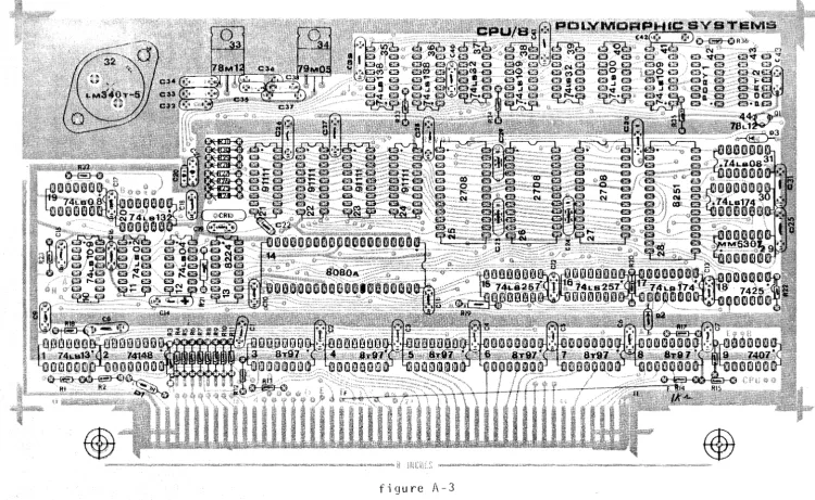
3. Assemble Processor Board
The central processor circuit card consists of the Inte18080A that provides all central processing, plus the devices that support the central processor: random-access and read-only memory, plus optional serial port if ordered.
Orient the board as shown in figure A-3.
a. Install components required for voltage regulation.
1. The following ICs are not dual in-line packages. Each of these ICs has a heat sink.
Check lCf! Part # Function
I:}
32 7805 or LM309 or LM340K-S.0 SV regulator(
. 33 78M12 12V regul a torNOTE: Insta 11 IC
34
with mica wafer and non-conductive screw.(~"
34 79M05 -5V regu 1 a tor(1
44
79L12 -12V regulator*PolyMorphic Systems POLY 88, Vol. I Rev. 0.0 PolS
2. Install the fo 11 owi ng capacitors.
CHECK CAP. # TYPE
(rf
20 10 ~F tantalum( f,;('
21o .
1 ~F ceramic disc('I(
32 through 35 10 ~F tantalum(1
36 and 37o .
1 ~F ceramic disc( . 38 .10 ~F tantalum
3. Now you can test voltage regulation. (/)Check pin 28 of IC 14 (CPU) for 12V+ 0.6 V.
(n
Check pin 20 for 5V:!.
0.25 V.(yf
Check pin 11 for -SV:!.
0.25 V. If proper voltages are not present, check the installed components and the solder points. Check continuity between IC 43 (78 MOS) and ground (outer trace); if resistance does not exceed 1,000 ohms, check the insulation on this IC. The metal tab should be insulated by the nylon screw and mica washer.b. Install integrated circuits. Begin by installing the
integrated circuits themselves, OR the optional sockets if you bought them.
If you bought the socket option, install and solder in place all sockets by referring to figure A-3 and the list of componenets below. DO NOT install the integrated circuits at this time; install them after completing Step C below. Verify the location of each socket by checking the number of pins. Verify that the orientation is correct by noting the "pin one" location on the figure.
PolyMorphic Systems POLY 88, V 0 1 . I Rev. 0.0 P . 16
CHEC K IC# TY P E #PINS FUNCTION
U{
1 74LS13 14 Quad NOR ga te(v( /
2 74148 lIP Decodery
(yf
3 through 8 8197 16 Bus driver( , 9 7407 14 Hex buffer
(~
10 74LS109 16(n-"
11 74LS02 14(v)"' 12 74LS04 14 Hex inverter
(vY" 13 8224 16 Clock genera tor
(vr'
14 So cke t 40 Socket for CPU(if
15 and 16 74LS257 .-lnt" if.:;.( iv)"
17 74LS174 -1-4-/t;.?(II"'(
19 ,~7rL.508 14(1/)' 20 74LS132 16
{/~
21 through 24 91 L 11 18 256X4 RAM{~
25 thro u gh 27 Sockets 24 Soc ke ts for ROM~,
*
{vY/
28 Socket 28 ' Socket for USART( 1"'"
1<6JrJ.S
,'I
*
(0'
29 MM 5307 ~t'f
Baud rate generator(0
30 74LS174 18*
(v)
31 74LS08 14(~
35 and 36 74LS138 1 6( vr'
37 74LS32 14 Quad NOR gate(vi'
38 74LS109 16(0'
39 74LS32 14 Quad NOR gate(:}
40 74LSOO 14 Quad NAND ga te~:y
41 74LS109 1 6,;>r. * 42 and 43 Sockets 14 Sockets for serial post
c. Ins ta 11 discrete components.
Ins ta 11 al1 resistors, starting at th e lower 1 eft cor n e r of the boa rd.
PolyMorphic Systems POLY 88, Vol. I Rev. 0.0
CHECK # TYPE
C~~
1 through1.'
2,200-ohm (red-red-red)(v(
1;L 4,700-ohm (ylw-viol-red)~*
13 :-11 r Q u-g;n ~ 1-22-+
:J. 3 2,200-ohml'+~1 1 ,000-0 hm (brn-b1k-red)
(/1"
1g
17r(U.17
2,200-ohm(:f
,~/S 1,000-ohm( )
1-9
through 28 2,200-ohm~;}
24 through 31 10,000-ohm (brn-blk-orng)32 through 36 2,200-ohm
Install all capacitors, starting at the lower left corner.
#
CH(EC}
vf "
1 through 7((vC
8V) 9 through 13
(yf'
14(0,
15 through 18(v(
19"-::::0==-,....;;:>-. ( ",.(" , 2 2 t h r 0 ugh 3 1
(r(:
39 through 42-,...(0
43TYPE
O. 1 ~F ceramic disc
470 pF ceramic disc
O. 1 ~F ceramic disc
33 ~F tantalum
O. 1 ~F ceramic disc
39 pF ceramic disc
O. 1 ~F ceramic disc
O. 1 ~F ceramic disc
10 pF tantalum*
P.
Install all diodes. Jhe end of the diode with the colored band (
points in the sa~e direction as th~ arrow etched on the board.
CHECK
(v('
->-(v(
#
1 and 2 3
TYPE
lN4148 lN4148*
17
If you bought the socket option, you can now check voltage
regula-tion without endangering your chips. Install the board into any
chassis edge connector (it will not go in wrong), then turn on the power and use a small voltmeter to verify +5V, +12V, -5V and -12V
(v('"
Xl Install 16.5888 MHz crystalPolyMorphic System~ POL Y 88, Vo 1. I Rev. 0.0
Install jumper using tel fan tubing from point labeled
"F"
near pin 21 On the edge connector to the corresponding
pOint "F" below
Ie
B.
If the power supply checks out, install all ICs now. ,If
power supply is not correct, fix it (check for solder 'bridges. mis-oriented components, etc.) before instal1.ing chips.
PolyMorphic Systems POLY 88, Vol. I Rev. 1.2 P. 19
4. Assemble Video Board
Install DIP sockets:
Orient the PC board so that the gold plated contact of the bus connector is facing you and the large foil area is at the upper right. This is the TOP of the board.
According to assembly diagram, check-off list, and designatlon on board, install sockets on top of the PC board.
Install IC sockets
Ch~' Location Comeonent
(' IC 1,2 16 pin sockets
(0"' IC 3, 4, 5 14 pin sockets
(~'" Ie 6 16 pin socket
(v}/
Ie 7 14 pin socket( t..y-""
Ie 8, 9, 10, 11, 12, 13 16 pin sockets~~
IC 14, 15, 16 14 pin socketsI C 1 7, 1 8, 1 9, 20 16 pin sockets
(t",,/
Ie
21 through 28 18 pi n sockets(Vf
r(>~9 It," "
(1/)
Ie
30, 31 , 32 14 pin sockets(0
Ie 33, 34, 35, 36 16 pin sockets(v(
IC 37, 38, 39 24 pin sockets(~'
Ie
40 20 pin sockets~. I C 41 24 pi n sockets
(~. IC 42 14 pin socket
(lr SWITCH DIP Switch
(t~-' J 1 14 pin sidewipe
PolyMorphic Systems POL Y 88, Vo 1. I Rev. 1.2 P. 20
Install res; stors Check
(<<~
( t,-y"
(vr/", ..
~.·
(~
"(~
7"'"
( ),,,/""'"
(V{ ~/
(/
(~
(1-1/
(vr
(
c;,1"~ (y((~.
(V)/'
(
v(.~(:{
Number Rl
R2 - Rl0 Rll R12 R13 R14 R15 R16 R17 R18 R19 R20 R21 R22 R23
R24, S,
R25
26
Descri ption
470 ohm 2200 ohm 1000 ohm 2200 ohm 1000 ohm
customer provided
red-red-red brown-black-red red-red-red brown-brad-red
option for keyboard (see page 28)
2200 ohm red-red-red
4700 ohm yellow-violet-red
2200 ohm 4700 ohm 100 ohm 220 ohm 220 ohm 82 ohm 2200 ohm 1000 ohm
3.300 ..11_
b.row.n:=bla ck --re d
yellow-violet-red brown-black-brown red-red-brown red-red-brown grey-red-black red-red-red brown-black-red
Install diodes: BEWARE OF POLARITY
C~7
~()
Install transistor Q-l
Step completed. (1--1""""
Install capacitors
(lY
Number Dl
02
Description 1 N5225
vacant (customer proyi ded
keyboard regulator)
eM
HEL/f.t.j
:IZ
2N5449 flat side toward top of board
Number C1 ,2 C3
C4 through C23
Description
O.luF Ceramic Disc Cap 100 pF ceramic disc
PolyMorphic Systems POLY 88, Vol. I Check (~. (~
(rr-~()>( )
(~(vY'-(~-"
(n
(~(W
(V('
(1/('-(t%~" (~--- (yY'-(t-{/Install potentiometers:
Number C24 C25, 26 C27
C28 option, customer provided C29 option, customer provi ded C30 C31 C32 C33 C34 C35 C36 C37 C38 ~'40,41 C42 C43,44,45,46
Rev. 1.2 P. 21
Description
lOl25V tantalum (note polarity) O.luF ceramic disc
lOl tantalum
O.luF ceramic disc (suggested)
lOuF 25V tantalum (suggested)
O.luF ceramic disc lOuF tantalum O.luF ceramic disc lOuF tantalum 39pf
22pf
.0047uF ceramic disc O.luF ceramic disc - lOuF tantalum - Note:
O.luF ceramic disc lOuF tantalum O.luF ceramic disc
positive toward bus connector
Install 10K ohm pots at R27 and R28. outside of board to be of practical value.
Screw adjustments must be toward
Step completed (~-.
Install Male output connector at Video out location.
Note that the unit closely matches the diagram printed on the Video board.
Step completed (~
/ /
Insta 11 vol tage regul ators /
At
Ie
43 install 12V regulator 78L12(£1(
check.PolyMorphic Systems POLY 88, Vol. I Rev. 1.2 P. 22
over the heat sink. Secure with 6-32 hardware. Solder underside after
securing heat sink. Check (~
4.a Smoke Test
At this point your VTI board is completed except for i.nstallation of IC's.
Before installing the IC's the board should be "srooke testedll• Connect
your VTr to appropriate power supply and observe carefully. Any unusual odor or sign of smoke indicates an error that must be remedied before you proceed.
4.b Install integrated circuits
Ch;?::" PINS FUNCTION
~/
IC 1 74LS161 16 Binary counterIC 2 74LS161 16 Binary counter
(/
.. IC 3 74LS02 14 Quad 2-input NOR gate(~/
IC 4 74LS74 14 Dual 0 flip-flop(~/
IC 5 74LS132 14 Quad 2-input NAND gate.~~.
IC 6 DM8131 16 6 input comparatorIC 7 74LSOO 14 Quad 2-input NAND gate
{~, IC 8 74LS153 16 Dua 1 4-input multiplexor
~~
IC 9 8097 16 Hex tri -state bufferIC10 8097 16 Hex tri-state buffer
(V~(
IC11 8097 16 Hex tri-state buffer(~': IC12 74LS138 16 3 to 8 decoder
(~
IC13 74LS161 16 Binary counter(/1'
IC14 74LS20 14 Dual 4-input NAND gate(Y}; ..
IC15 74393 14 Dual 4 bit binary counter7f~1J
(~
IC16@>~
14 Dual 4 bit binary counter(.f
IC17 74LS157 16 Quad 2-input multiplexor(~
lC18 74LS157 16 Quad 2-input multiplexor(H-. IC19 74LS157 16 Quad 2-input multiplexor
PolyMorphic Systems POLY 88, Vol. I Rev. 1.2 P. 23
Check PINS FUNCTION
~
lC21 91 L 11 18 256X4 bit static memory(vi' lC22 91 Lll 18 256X4 bit static memory
(~ lC23 91 Lll 18 256X4 bit static memory
memory opti on
(0
lC24 91 L 11 18 256X4 bit static memorymemory opti on .
(v( IC25 91 Lll 18 256X4 bit static memory
memory opt ion
( i/)/ lC26 91 Lll 18 256X4 bit static memory
memory option
(I~· lC27 91Lll 18 256X4 bit static memory
(y) IC28 91 Lll 18 256X4 bit static memory
..
(tf
lC29 74S124 16 Dual gated voltage contrid osc.(~. lC30 74LSOO 14 Quad 2-input NAND gate
(t.-r
lC31 7407 14 Hex open-coll ector buffer(~ ....
lC32 74LS74 14 Dual D flip-flop
(~ lC33 74LS157 16 Quad 2-input miltiplexor
(q"
lC34 74123. 16 monostable multivibrator~~
lC35 N8274 16 Ten bit shift registerlC36 74LS157 16 Quad 2-input miltiplexor
(~ lC37 MCM6571 A 24 Character generator
(q/
lC38 74150 24 16-input multiplexor(...y'"
IC39 74150 24 16-input multiplexor(~ .. lC40 74273*
20 8 bit register
(t-Y
lC41 74S412 or 24 8 bit latch8212
(~ lC42 74LS132 14 Quad 2-input NAND gate
4. c Opti on Sel ecti on
Though the VTl is an integral part of the POLY 88 system, it is compatble with other systems. We have therefore, included a number of additional jumper option areas which do not apply to POLY 88 owners.
These are Jumper areas 1, 2, 3, 5 and 6.
PolyMorphic Systems POLY 88, Vol. I Rev. 1.2 P. 24
JMPl changes the divide ratio from the system clock to produce scan rates which are more appropriate when using
different system clock rates.
JMP2 selects the vectored interrupt priority for the
keyboard input. The VTI is already wired for interrupt
priority 2.
JMP3 and JMP6 are similar to JMPl in that they adjust the scan rates when used with different clocks.
JMP5 allows use of an on-board clock.
4.d Select Character line length option.
Your board is configured for a 64 character line. If
you require the 32 character line cut the trace on the back of the board between the middle pad of JMP4 and the pad designated
64 at JMP4. If you do not require the 32 character line, do
nothing.
4.e Address location:
The VTI interacts through the 5-100 bus as a block of
memory and input port for keyboard. The memory block, (~or K
bytes, depending on option) can be located at any address from
o
through 63 K in 1 K increments. (Software writter for thisproduct will usually locate it at hexadecimal address FaDD).
Location is determined by comparing the six most
significant bits of the memory address with six jumper selected
bits. Reducing circuit co~plexity, the memory block also
PolyMorphic Systems POLY 88, Vo 1. I Rev. 1.2 P. 25
significant bits of the input port address must match
the six switch or jumper selected bits. The two least
signifi-cant bits are not compared for input address therefore, their state is arbitrary.
The address selection switch area is located at the lower
left hand corner 6f the board near Ie6.
Each of the six most significant bits of the address is
resistor tied to + 5V, so that they are normally in binary
state l. Any or all of them may be grounded to cause a
situation of binary state
0.
A DIP switch is provided forselectable jumpering. Typically, the address line on the right
is grounded to the pads at left, producing a logical zero. The
five switches nearest bus connector should be in the off
"--.---~--,~.--,--~~., ,. --" --_ .. - ----".-~-... ---.~---...
--.---po sit ion . The rem a i n i n g two s wit c h e s s h a u 1 d be 0 n. s e tti i!9 __
J_IlE;
- - - -..
--~.--... -.. -... - .. -.---.--.
DoaraatTg~0 H ,
&'3'1
gg
4 . 3 I n t e r fa c e TV m 0 nit 0 r 0 r T V r e c e i v e r : .---- .. J .
b.
At this point, your unit should operate if connected via coaxial cable to either video monitor or slightly modified
receiver. (For the Hitachi line, an inexpensive TV receiver
modification kit is available through PolyMorphic Systems). If the prompt character does not appear on "power up", horizontal frequency adjustments, found on the back of the video unit, may be required.
Because of rigid FCC regulations, the circuit has been designed for direct connection to the video input circuit of the video amplifier, which is located between the last video IF
stage and the video output circuit.
When the circuit is broken atvideo amplifier input, a DC bias circuit for the stage will probably be necessary, since
in most cases it is supplied from the video IF amplifier. The
optimum interface circuit will vary, but frequently a
PolyMorphic Systems POLY 88, Vo 1. I Rev. 1.2 P. 26
The coupling capacitor is typJcally a 1~5uF tantalum, oriented
'with the positive side connected to the video input amplifier.
IMPORTANT: Check to see that the cha~sis of your TV is
isolated by a transformer from the 110 VAC line. If the
chassis is not so isolated, but rather a polarized plug h~s
been used on the line cord, FATAL INJURY COULD RESULT from
possible electrical shock. If you must use this type of set,
either isolate it with a transformer or isolate the video signal with an opto-isolator between the video terminal
interface and the video input connection to the TV set~ Under
no circumstances should the polarized plug be trusted to main-tain the isolation from the line voltage.
4.4 Connect key~oard
At the upper right hand corner of the video terminal
inter-face board is the keyboard input port. This port provides a
latched 8 bit parallel input capability which completely
inter-faces with>omany ASCII keyboards. Keyboards usually indicate
a keystrike to the computer via a strobe line, in addition to
the eight parallel input lines. The signal on this line changes
state -- from high to low or from low to high -- to indicate a
keystrike. Hookup varies according to whether the strobe on
your keyboard is "positive going" (rising in voltage to
indicate keystrike) or II nega tive going" (dropping to indicate keystrike).
4.4.1 Connector configuration
The parallel input from the keyboard is designed to come in over a ribbon cable terminated by a DIP MALE CONNECTOR. This plugs into the 14 pin DIP socket at the upper right hand
corner of the board. The 8 parallel input lines are connected
to pins 1 through 8 of this socket, (J-l) with 1 being the
least significant bit. Pin.9 carries the IIpositive goingll or
PolyMorphic Systems POLY 88, Vo 1. I Rev. 1.2 P. 27
Pin 13 is the output from the optionc}l Gne~ati,ye voltage
regulator, Pin 14 carries +5 volts as the primary supply for
most keyboards. JMP8 allows 8 volts unregulated power at Pin 14
if desired. Be sure to cut the trace connecting 5 volts if you
require this option. A jumper is inserted from the middle pad
of JMP8 to the pad nearest the regulator within the area designated JMP8.
WARNING: FAILURE TO CUT THE TRACE SUPPLYING 5 VOLTS WHILE ATTEMPTING TO JUMPER IN 8 VOLTS WILL DESTROY EVERY COMPONENT ON THE BOARD AND VOID THE WARRANTY!
4.4.2 Keypress strobe
When the processor accesses the video terminal interface with an input instruction, the state of the keyboard input
latch is transferred to the accumulator. Proper use of the
keyboard requires that the processor must establish two
conditions before using the input data. It must indicate that
1) a key has been pressed, and
2) this particular key depression has not been
previously serviced.
These functions are accomplished by making the keypress strobe information available to the processor.
The keypress strobe line is an additional keyboard output
line parallel with the data lines. This line signals each
depression by a pulse. This test-function informs the processor
that the necessary input conditions are met. The pulse:
1) interrupts the processor by setting an interrupt
service latch contained on the input buffer,
-~Used when the keyboard requires a negative supply. The user should
PolyMorphic Systems POLY 88, Vol. I Rev. 1.2 P. 28
or 2) the interrupt request latch is available on data
bit
0
of the status port; the keyboard strobe is availableon data bit 7.
Attaching the strobe line of your keyboard to a YOM determine
whether it is normally low (below .8V) or normally high (above 2.5V). If
low, the jumper is already properly configured.
If high, cut the minus trace from center pad of JMP-7 and jumper
from center pad to + labled pad.
i. optional voltage regulator
Provision has been made for the optional negative voltage regulator required by a number of keyboards. The pads and traces for this voltage supply are located adjacent to the keyboard input socket, just above the
IC23. The supply regulates the -16V line by means
of a resistor and zener diode stabilized by two capacitors. The four components are R14, C29, C28 and 02. The choice of resistor and zener values depends on the voltage and current requirements of the keyboard.
5. System checkout.
Install all boards and IIsmoke testll them. If something is obviously
wrong, solve it before proceeding.
To test the POLY 88 system, you will want to hook it up to the video monitor.
In addition to a video monitor, you will need a simple logic probe with pulse detector. If you do not have one, buy one or build one using the
circuit enclosed. If you cannot use a logic probe, do not attempt
detailed checkout.
You will also need the VTVM or YOM you used earlier. A magnifying glass will also be helpful.
If the system does not operate properly, first eliminate the m~st
PolyMorphic Systems POLY 88, Vo 1. I Rev. 1.2 P.29
( ) 1.
() 2. () 3.
() 4.
() 5.
Check all components on all boards for proper location and orientation. In particular, check the tantalum capacitor orientation carefully.
Check all boards to make sure there are no solder bridges. Check that all jumpers are in place, and that they are correct for either the 32 or 64 character option, whichever you ordered. Check all boards to make sure tha all IC pins are correctly inserted -- not folded under or broken off, etc.
•
Check the jumpers or DIP switch on the video board for proper address selection.
If these problems are eliminated and the system still does not run properly, check the CPU board, using the logic probe pulse detector, to ensure that the clock signal from IC13 is available on pin 49 of the edge connector.*
If there ;s no clock signal, check for solder bridges and incorrect component placement and orientation on the CPU board. Check 1C13 and 1C8 (bus driver, 8197) using the list of chip pinouts at the end of this
volume. Pins 10 and 11 of IC12 should have +2 to +8V. Use a VTVM for this
test if your logic probe will not accept these levels. A malfunction at this point will usually produce a constant OV or 1 OV. If you now have a clock pulse on pin 49 of IC13, and you still have system malfunctions,
proceed to Video Board checkout, immediately below. If you still do
not have a clock pulse, go directly to CPU Board checkout.
a. Video Board Checkout
If you have a clock signal, hook up the video monitor and power up. You
should get a clear screen with the cursor in upper left hand corner.
The video board consists in essence of three areas: Sync, Data Bus, and Character Generation-Video.
If you have a coherent, stable, but useless display, the problem is most likely in Data Bus.
PolyMorphic Systems POLY 88, Vol. I Rev. 1.2
P.
30 If you have no display, the problem is most likely in Character Generation-Video.One problem that affects all three areas is the output buffer, so begin by checking pinouts on:
() IC 31 (output buffer, 7407).
Next, perform the relevant steps below. Oata Bus
( ) Check all RAMs, ICs 21 through 28 (91l11 or 2111).
() Check all
RAM
pins for proper insertion() Check for solder bridges on RAMs and in the bus driver area. Character Generation-Video
( ) Check the dot clock chip, IC 29(74S124).
If you have a display, you can check IC29 by decreasing the display
width by adjusting potentiometer R27. If the display changes, the
dot clock chip is probably defective.
() Check the shift register, IC 35 (8274).
If you have done all the above, and still have system malfunctions,
continue with detailed checkout below. If a synchronized array of
characters cannot be achieved by adjustments of sync controls on the CRT (or TV), check first for the more obvious and frequently encountered problems. Most typical will be such items as:
1. loose connections to system or to display.
2. Improper interfacing to display's video input (biasing, etc.).
3. Omission or improper installation of components on the board (reversed diode or chip orientation).
4. Soldering problems of unsoldered contact or solder-bridge shorts.
5. Omitte~ or wron91y selected jumper patterns (line length, address
selectlon, etc.).
The discussion below follows one of many possible logically
sequenced procedures to localize problems and is written for those without access to an oscilloscope.
PolyMorphic Systems POLY 88, Vol. I Rev. 1.2 P. 31
board itself. Progress through checks on the power supply
busses and video output to electrical test patterns of the
signals on the board. In using the electrical test patterns,
work from end results backwards towards those parts of the
circuit which contribute to the end results. For example: if
the proper raster sync signals are doing their job, all further measurements concerning these circuits involved can be omitted in favor of checking contributions to character presentation.
a. 1 Power rna ins
a.1.1. If visual inspection looks good, see if the power mains
are proper. There should be +5.0 + 0.2 VDC on the VCC bus.
Convenient clip lead points include:
A. Ground reference: the metallized board area under the
voltage regulator heat sink at the top right is a good one. The
board has been designed with a blank area on the reverse side
sot hat the 0 the r jaw 0 f a c 1 i p ca n not s h 0 r tan y s i 9 n a 1 s
(Watch out for this at other locations, especially along
B. 5 volt bus: the bottom lead of resistor R12. A
there. the top of
th e bo a rd.)
voltage below tolerance here may indicate either a heavy current load from a misconnection or a reverse-oriented IC or that your
power main feeding the board has less than 7 volts available.
Zero volts at this point probably indicates missing power to the board (a cold regulator) or a dead short on the board in
which case the regulator will be very hot to touch. (Oon1t
panic. You will be amazed at its recuperative capability when
the short is cleared.)
C. VOD bus for the character generating ROM 1C36(6571-4).
Measure +12V+ 10% at the junction of R20jC29.
D. VBB bus for IC37: Measure -3V + 10% at the left hand lead
of 01. (This is the only negative voltage.)
a.1.2 If power bus shorts are suspected, ohmmeter verification
PolyMorphic Systems POLY 88, Vol. I Rev. 1.2 P. 32
board will not suffer from checks where the ohmmeter leads apply the polarity expected from the power supply and an open circuit
voltage not exceeding the power supply value. The non-linearity
of the load prevents us from predicting what an unknown ohmmeter will read on a normal board, but readings below an ohm mean that
you should look for a short or an inverted IC. Reverse polarity
from ohmmeter leads can be damaging unless the current is l~mited
to low values. Most ser1es-connected 50 micro-amp movement VOM's
are safe when only the 1.5 volt battery is used on the scale selected.
a.2 Signal tracing
Unsolder the right end of the 100 ohm Rl
4, 6, of IC3l----7407) and attach a clip
of the resistor for use as a scope orobe.
(junction with pins 2, 1 e ad to th e f r e e end
(Keeping a wire in
the hole for the right end of R18 makes an easy way to remake the IInormal" connection with the clip lead.)
DC voltages would normally read 1.6 V at this junction, but, when open, the clip lead will read about 4.5 and the IC31(7407)
pins less than 0.1 V. This produces DC levels at the 2N5449
emitter of about 2V normally (average of normal waveform) and
near 4V with an open test lead. 27% of these values should be
found on the cable to the CRT. (If you have D.C. coupled into
your CRT video, check that your deSign is proper for these values.)
Those users owning oscilloscopes probably have sufficient
technical background to interpret the following discussion into
equivalent scope presentations. This discussion assumes that
the only signal tra~ing display available is the TV or CRT
intended for computer display use. Therefore, the first checks
are that the output stage is functioning and that its responses
are visible on the CRT. If NOGO on these, check your cable and
PolyMorphic Systems POLY 88, Vol. I Rev. 1.2 P. 33
a.2.1 video interface
Grounding the probe lead should pull the output emitter down to around a volt, and opening it should give a rise to around 4v. This transition should couple through the AC coupling to your CRT and be apparent as momentary brightening as the lead opens.
a.2.2 localizing on the video path
If logic levels applied to the clip lead are modulating the dis-play brightness, but you are having to troubleshoot, let us
consider what is missing. If, in the "normal" connection (i.e:
lead clipped to where R19 should be soldered), there is an array of bright and dark spots on the display, chances are that video is being generated and that you will be chasing sync or blanking
troubles. With only video coming through, most CRTs will at
least partially sync on the video itself, and patient tinkering with the sync controls on the display and the two pots on the video board should give at least some torn-up version of what is
trying to be a display. If you have sophisticated your power-up
sequence to program a blank display, either alter the sequence until troubles are cured or remove programming to the board. Random states in the board RM1 at power-up will produce some
interpretable static pattern. But maintain the system clock
connection. Horizontal sync is derived from that clock. (The
board is testable with nothing more than proper power supplies and a clock for inputs.)
No video pattern? Let us see if it is shifting out of the
register rC35-6(8274) (pin 6 of IC35). Got it? Then the path
through 1C31 is not passing i t . Check for it at the input pin 9
and 0 u t put pin 8 a f I C 31. F 01 1 a vJi n g the path s h 0 u 1 d rev e a 1 a
gap in signal passage that is correctable. This is the concept
of signal tracing that wi1l be assumed throughout the remaining discussion.
PolyMorphic Systems POLY 88, Vol. I Rev.1.2 P. 34
inp~t pins to be loaded for shifting - or a load signal to load
it - or a dot clocking to shift it out?
First the dot clock on 1C35-9(8274): This should show as
a raster full of tiny white dots. Depending on the
setting of the "widthll pot, there should be from 100 or so to
a.l mas t this. out of
900 on each raster Sync and blanking, the visible area.
sweep, but several factors influence if they are working, keep many dots Also, the bankwidth of this setup may not permit you to discern dots at the higher frequency settings
of the dot clock. Best to view this at the minimum frequency
(ccw) setting of the IIwidthll pot (pot at top left). Do not
bother counting dots. Their presence is all that is n~cessary
to show register shift clocking input. Since this signJl is
negative true, a brighter presentation may be found at the
inverted form on IC30-8(74LSOO). Absence of sync should
not prevent this display from being recognizable.
EOC (end-of-character) loading signals on 1C35-7 should show as dark (nega tive true) verti cal bars every tenth dot
(except for a portion of the screen where horizontal blanking
normally disables the dot clock). T~eir presence proves the dot
clock (and dot counter) whether we check 1C35-9(8274) or not. The number of bars visible is variable by the dot clock frequency
("width" pot) and by the "pas" pot control of sweep blanking.
Although the blanking path is broken by lifting R19, the composite
sync path is not. Therefore, if a strong sync is at work, some
of the display, such as the area unbroken by vertical bars, may be
sync'd into times not visible on the screen. This point about
sync must be borne in mind as you check many of the waveforms -particularly in the sync path itself.
Assuming that shift (dot) clocking and its subcount. EOC load clocking, are available, is there video data on the input pins
to be loaded? Each of. pins 1 through 5 and 11 through 14 should
PolyMorphic Systems POLY 88, Vol. I Rev. 1.2 P. 35
distance between the vertical bars seen on pins carrying the EOC
or shift loading pulses. So too should input and output pins of
the MUX's IC33 and IC36(74LS157}. Also the outputs ROM
IC37 (6571) and the graphics generators IC3~ and IC39(74150).
The patterns associated with outputs from IC38 and IC39(74l50)
have a right to change every 5 sweeps. At the IC39(74273) inputs
to the display generators IC37, 38, & 39, (6571) however, the
sweep patterns should not change more frequently than every
fifteenth sweep. These last patterns show what the memory is
requesting for each character position of ten dots by fifteen
sweeps. Counting these dimensions is generally not necessary.
I~erely noting that the fineness of detail is less at the input to generators than at
trouble local1izing. and 3.2.5.
the output is usually sufficient for Subcounting is discussed under 3.2.3
The screen pattern for any significant bit input to the generators should be traceable back through corresponding pins of the
sampling latch IC40(74273) to the same significant bit of
the internal data bus. But remember, the nth character in
memory is held in the latch until an EOC pulse strobes the latch
and increments the memory address. If sync and clocking are at
work to keep the display pattern straightened up, any lack of correspondence of the patterns up the path can be discerned. Without sync, it may take both a photographic memory and a lot of luck -- but the chances are that you \.."ould not be needing that level of detailed trouble-shooting without sync, anyway.
In like fashion, grounding pin one of IC33(7LS157) forces NUX's IC33 and IC36(74l51) to select only graphic symbols from IC38
and IC39(74l50). This change is most apparent with a sync'd
display, but some shift should usually be discernible in the
pattern for any shift register input pin. The degree of change
PolyMorphic Systems POLY 88, Vol. I Rev. 1.2 P. 36
which memory locations contain graphics or non-graphics characters. An MSB in memory is inverted in the latch to select graphics.
a.2.3 localizing on the EOC (end of character) path
If you had dot clock input to shift register IC35-9(8274) but no
stobe (IC35~7) to load the register, you will want to check back
to where the
Eoe
is generated by counting every tenth dot inlC14. In fact, failure of IC30~74LSOO) or other problems can
permit it to count by other than ten, wi th some weird results in
displays. Clock dots are discernible at the input lC13-2.
Slow-i n 9 th e dot c 1 0 c k (e e Won the II. wid t h" pot) m a k est he sec 0 u n tab 1 e
by eye. A piece of paper on the screen or a millimeter scale
may help. Sync helps here but should not be necessary to array
the pattern of dots into vertical bars. lC13-l4(74161) has half
as many vertical bars but of double width. Pin 13 has narrow
v e r tic a 1 w hit e bar seq u a 1 to tw ice the wid tho f the bar son
pin 14. The total pattern of pin 13 is repetitions of black,
white, black, White, white vertical bars. The last two whites
show as a double width white as the carry pre10ads a 6 into
this 4 bit binary counter. This preload makes it produce a
carry every tenth dot. If pin 13 looks right, chances are
that a 11 the res t ; s 0 kay.
The tenth dot carryon lC13-15 is the EOe (end of character)
signal. It should appear at the input to the symbol counter
IC16-13. An inverse (negative true) of this pattern should
be found as loading signals n latch lC40-11 (74273) and shift
register lC35-9. Of course, if there is no dot clock, none
of this paragraph is working properly. On the other hand,
presence of dots anywhere does not leave much room for problems in the dot clock.
a.2.4 localizing on the dot clock path
PolyMorphic Systems POLY 88, Vol. I Rev. 1.2 P. 37
clock is present at the other end of these places. If neither
is present (and of cou~se no EOC signals), then look for dots
at the clock 1C29-7(745124). Using a voltmeter, check its "width"
pot for the abil i ty to vary 1C29-2 from zero to 5 vol ts. Check
also for the ena~ling portion of the horizontal blanking signal
on 1C29-6. This may be hard to see as a broad vertical bar in
the presence of strong horizontal sync, but if desyncing gives
you a torn version of it, it is probably okay. A voltmeter
reading on 1C29-6 of S VDC would be a continuous disable signal. Under proper conditions, the average of the horizontal blanking waveform reads typically 0.9 to 2.3 VDC on a meter at 1C29-6. The value is under control of the "pOSIl pot which varies the time delay (and thus the average DC value) of the blanking monostable.
a.2.S localizing on the horizontal blanking path
Under the most ideal conditions of sync and blanking, events occurring during flyback, retrace, or blanking should not be
visible. Note that opening R19 does not open the composite
sync path at 1C3l·10(7407). Therefore, sync, if operating, will
reach the CRT sync circuits - regardless of what is done with
the probe lead. Remember, even without sync working, most CRT's
or TV;s will find in many of the test signals something repetitious
enough to sync on. There is usually a way to view sync-hidden
signals by misadjusting the horizontal hold control of the CRT to
force a "tearll in the picture. Then if the sweep rate is
calibrated in time units, the Signal can be measured in the torn
portion. An example of this is horizontal blanking. Forcing a
torn but stable pattern reveals a dark space in each sweep when
looking at 1C29-6 (74$124). Varying the "pos" pot changes the
width of the space.
Typical values from stop to stop on the pot are about 10 or 20 microseconds (see section 3.'3.1 on time calibration) but, if you
Po lyMorphi c Sys tems POL Y 88, Vol. I Rev. 1 .2 P. 38
inverse - a logic high on 1C34-5(74123). For this, you should
not have to force the tear. Horizontal blanking that is high
logic will appear as a bright vertical bar at one or both sides
depending on where the CRT is syncing. For most IC's, if Qis
working, Q probably is also. Take the easi·est way down the
locallizing path first and back up to the harder ones only when necessary.
No horizontal blanking? How about the horizontal sync which
triggers the 1C34 monostable multi-vibrator to stretch the sync
into a wider blanking? The carry out of counter ICl-15{74l61)
should have its inverse on 1C34-9(74123). This is a 4~
micro-second pulse every 58~ microseconds.
Actual horizontal sync is the same width, but 4~
mi croseconds 1 a ter, and can be seen on 1C3 -13 (74lS02) . Its
inverse is on 1C3-1 but is also mixed with vertical sync. Observation of a once-per-sweep, narrow vertical bar is
probably sufficient to eliminate further details.up this path, but if things are not clearing up, you may want to calibrate time as in a.3.1.
If these are NOGO, is the system clock on edge pin 49 and is it reachinq lC2-1(74161)?
You can use your piece of paper or plastic millimeter scale
to ratio