61 00 Disk Controller
User's Guide
PB61 00-9001-02
®ISYFifEM
INDUSTRIES
Milpitas, CA 95035, USA 1855 Barber Laneii
System Industries has prepared this manual for use by System Industries per-sonnel, licensees, and customers. The information contained herein is the property of System Industries and shall neither be reproduced in whole nor in part without prior written approval from System Industries.
LIMITED WARRANTY
Disk Controller. System Industries warrants that its products are free from defects in materials and workmanship and meet System Industries' performance specifications. The warranty period is ninety (90) days from the date of shipment to Buyer. This warranty is limited by the paragraphs below.
Return to Factory. If Buyer discovers a defect in a System Industries product covered by this agree-ment, Buyer's exclusive remedy is to ship the product back to System Industries' Milpitas factory where System Industries will, at its option, either repair or replace the product. This remedy applies if System Industries receives the returned product on or before the tenth day after the expiration of the warranty period and Buyer n\;,tifies System I ndustries of the defect before returning the product.
Cost to Buyer of Repairs or Replacement. Buyer must prepay freight charges to System Industries. System Industries will pay return freight to Buyer. There is no other charge for repair or replacement during the warranty period.
Transferrable Disk Drive Warranty. In addition to the foregoing warranty, System Industries also provides to Buyer the transferrable warranty, if any, provided to System Industries by the disk drive manufacturer. (NOTE: Neither System Industries nor disk drive manufacturers warrant read/write heads or subsequent damage sustained as a result of head/disk interference. Head/disk Interlerence can be prevented by carefully following the disk drive and disk pack manufacturers' recommended operating and preventive maintenance procedures.)
Limitation of Warranty and Liability. The foregoing constitutes System Industries' entire warranty, expressed, implied, andlor statutory (except as to title), and states the full extent of System Industries' liability to Buyer or to any other party for any breach of such warranty and for damages, whether direct, special, incidental, or consequential. OTHER THAN AS EXPRESSLY PROVIDED IN THIS DOCUMENT, NO WARRANTIES, EXPRESSED OR IMPLIED, INCLUDING ANY WARRANTY OF MER-CHANTABJLlTY OR FITNESS FOR A- PARTICULAR PURPOSE, ARE MADE. NO EMPLOYEE, REPRESENTATIVE, OR AGENT OF SELLER HAS ANY AUTHORITY, EXPRESSED OR IMPLIED, TO ALTER OR TO SUPPLEMENT THE TERMS OF THIS WARRANTY.
I
ILIST OF EFFECTIVE PAGES
Changes, deletions, and additions to information in this manual are indicated by bars (I) in the margins. A bar by the page number indicates pagination rather than change of page content.
PAGE REVISION PAGE REVISION PAGE REVISION
1-1 through 1-4 02
2-1 02
3-1 through 3-3 02 4-1 through 4-10 02 5-1 through 5-3 02 A-1 through A-22 02 B-1 through B-3 02
I
I
i
I
I
I
REVISION RECORD
REVISION
DATE DESCRIPTION EO
NUMBER NUMBER
01
9/08/81
Initial Release-02
2/23/82
Pages Affected: All 1504PREFACE
This manual contains sufficient information to enable the end user to install, test, and operate the System Industries 6100 Single Board Disk Controller.
The technical contents of this manual have been prepared based on the following assumptions of reader knowledge:
1. The reader should have a working knowledge of Digital Equipment Corporation PDP-11 processor hardware.
2. The reader should be familiar with disk structures and hardware.
3. The reader should be familiar with standard installation, power, grounding and peripheral cabling procedures.
The information in this manual is presented in five major sections. The contents of these sections are as follows:
Section 1.0
Section 2.0
Section 3.0
Section 4.0
Section 5.0
System Overview, describes 6100 board features, capabilities, and system configurations supported.
Physical Description, describes and illustrates the 6100 Controller PCB.
Functional Description, describes and illustrates the functional operation of the 6100 board.
Installation, describes and illustrates the procedures required to install the 6100 board and cable the drives.
Diagnostics, describes the diagnostics compatible with the 6100 Controller.
Other publications applicable to the 6100 Controller are as follows:
Publication Number Title
N/A PDP-11 Processor Handbook
EK-RM023-UG-002 DEC® RM02/3 Disk Subsystem User's Guide
64712400 CDC Flat-Cable Interface Specification for SMD, MMD, and CMD
Families
64709300 CDC Product Specification for the Flat-Cable Interface Storage
Module Drive Family
B03P-4580-0100B Fujitsu M228X Fixed Disk Unit Customer Engineering Manual
83322200 CDC Storage Module Drive BK4XX, BK5XX Hardware Reference
Manual
83322320 CDC Storage Module Drive BK6XX, BK7XX Hardware Reference
Manual
PB9901-9001-01 System Industries Disk Drive User's Guide
DEC is a trademark of Digital Equipment Corporation.
TABLE OF CONTENTS
1.0 SYSTEM OVERVIEW ... 0 0 0 • 0 0 0 • 0 0 0 0 0 0 0 0 0 0 0 0 • 0 0 0 0 0 0 0 0 0 0 0 0 0 0 0 0 0 1-1 1 . 1 Features. 0 0 0 • 0 0 0 0 ' 0 • 0 • • 0 0 0 0 0 0 0 • 0 0 • 0 0 0 0 0 0 • 0 0 0 • 0 0 0 .0 0 0 0 • • • • • 0 0 • 0 0 • 0 0 0 1-1 1.2 Configuration 0 0 0 0 0 • 0 0 • • 0 0 0 0 0 0 0 • 0 • • 0 0 0 0 0 0 0 0 0 0 • • 0 0 • • 0 0 0 • • 0 0 0 0 0 • 0 0 0 • 0 1-1 1.2.1 Software Compatibility .. 0 0 • • 0 • • 0 • • 0 0 0 • 0 0 0 0 • 0 • 0 • 0 0 • • • 0 0 • 0 0 • 0 0 0 0 1-1 1.2.2 Drive Configurations 0 0 0 0 0 0 • 0 0 0 • 0 0 • 0 0 • • 0 • 0 • 0 0 • 0 0 0 0 0 • • 0 • • • 0 0 • 0 0 0 1-2
2.0 PHYSICAL DESCRIPTION 0 0 0 • • • 0 0 0 0 0 0 0 0 0 • 0 0 0 • 0 • 0 0 0 0 0 0 • 0 • 0 0 0 0 0 0 0 • 0 0 0 0 • 0 0 0 0 2-1 2.1 Power Requirements 0 0 • 0 0 0 0 0 0 0 • 0 0 0 0 0 0 0 0 0 0 • • 0 0 0 0 0 0 0 • 0 0 0 • • 0 0 0 0 0 0 0 • 0 0 o. 2-1 2.2 Drive Interface 0 0 0 0 0 0 0 0 0 0 0 0 • 0 0 0 0 • 0 0 0 0 0 0 • 0 • 0 0 0 0 • 0 0 0 0 • • 0 0 0 0 0 0 • • 0 0 0 0 0 0 2-1 2.2.1 A-Cable 0 0 0 0 • 0 0 0 0 • 0 0 0 0 • 0 0 0 0 0 0 • 0 0 • 0 0 0 0 0 0 0 • • 0 0 • 0 0 • 0 0 0 0 0 • • 0 . -• • 0 2-1 2.2.2 B-Cable ... 0 • • 0 0 • • 0 0 • • 0 0 • • • 0 • • 0 0 0 0 '0 0 0 0 • 0 0 0 0 0 0 • 0 • 0 0 • 0 0 0 • 0 0 0 0 0 2-1 2.3 Computer Interface 0 0 0 0 0 0 0 • 0 0 0 0 0 • 0 • 0 0 0 0 0 0 0 0 0 0 0 • 0 0 0 0 0 0 0 0 0 0 0 • 0 0 0 0 • 0 0 • 0 2-1 2.3.1 UNIBUS Interface. 0 • 0 0 0 0 0 0 0 0 0 0 0 • 0 • 0 0 • 0 0 0 0 0 0 0 0 0 0 0 0 0 0 • 0 0 0 0 0 0 0 0 0 2-1 2.3.2 Device, Interrupt, and Address Configuration Switches 0 0 0 0 0 0 • 0 0 0 0 0 0 0 0 0 0 2-1
3.0 FU NCTIONAL DESCRI PTION . 0 0 • 0 0 0 • 0 0 0 0 0 0 • 0 0 0 0 0 0 0 0 • 0 • 0 0 0 0 0 0 0 0 0 0 0 0 0 0 0 0 0 0 0 3-1 3. 1 Priority Levels o . 0 • 0 0 • 0 0 0 • • • • • 0 0 0 0 0 0 0 • • 0 0 0 0 0 0 0 0 0 0 0 0 0 0 0 0 0 0 0 0 0 0 0 • 0 0 0 0 0 3-1 . 3.2 Overlapped Seeks 0 • 0 • • 0 0 • 0 o . 0 • 0 0 0 • 0 0 0 • • 0 0 0 • 0 • • 0 0 0 0 0 0 0 0 • o· 0 • • 0 0 0 0 0 0 o . 3-1
3.3 Dual Port Drive Compatibility 0 0 0 0 • 0 0 0 0 0 0 • 0 0 0 0 • 0 0 • 0 0 0 0 0 0 0 • 0 0 • 0 0 • • 0 0 0 • • '0 3-1 3.4 Contiguous Transfers. 0 0 0 0 0 0 0 0 0 0 0 0 0 • 0 0 0 0 0 0 • 0 • 0 0 0 0 0 0 • 0 • 0 0 0 0 0 0 • 0 0 • • 0 0 0 0 3-1 3.5 RPS Look-Ahead o . 0 • 0 0 0 0 • 0 0 0 • 0 0 0 0 • • 0 0 • • • 0 0 • • • 0 0 0 0 0 0 0 0 0 0 0 0 0 0 0 0 0 0 0 o· 0 0 3-1 3.6 Search Command 0 0 0 0 0 0 0 0 0 0 0 0 0 0 0 0 0 0 0 0 0 0 0 0 0 0 0 ' 0 0 • 0 0 0 0 0 0 • 0 0 0 0 0 0 0 0 0 0 0 0 0 3-1 3.7 Error Correction 0 0 0 0 • 0 0 0 • • 0 0 0 0 0 0 0 0 0 0 0 0 0 0 0 0 0 0 0 0 0 0 0 0 0 0 0 0 0 0 0 0 0 0 0 0 0 0 0 0 0 3-1 3.8 Controller Registers 0 0 0 0 • 0 0 • 0 0 0 0 0 0 0 0 • 0 0 0 0 0 0 0 0 0 0 0 0 0 • • • 0 • • 0 0 0 0 0 0 • 0 0 0 0 o . 3-3
4.0 INSTALLATION 0 0 • • • 0 0 • • • 0 0 0 0 • • • 0 0 • • • • • 0 • 0 • • • 0 • '0 0 • 0 • • • • 0 0 • • • 0 • 0 0 • 0 0 0 0 • 0 4-1 4.1 Visual Inspection ... 0 0 0 0 • • • 0 0 0 0 0 • • 0 0 • 0 0 • 0 0 0 0 • • 0 0 0 0 • 0 • • 0 0 0 0 0 • 0 0 0 0 0 0 o. 4-1 4.2 Switch Settings 0 0 • 0 0 • • 0 • 0 • • 0 • • 0 0 0 • 0 • • 0 • 0 0 • 0 0 • 0 0 0 0 • • • 0 0 0 0 0 0 0 0 0 0 • • 0 0 o. 4-1 4.2.1 DMA Throttle Count Switch 0 0 • • • 0 0 • 0 0 • • • 0 0 0 0 0 ' • • 0 0 0 0 0 O. 0 0 0 • • 0 0 • • 4-3 4.2.2 Register Set Address Switch (CS1) 0 0 0 0 • 0 • 0 0 0 • 0 0 0 0 • • 0 0 0 • • 0 • 0 0 0 0 • • 0
o.
4-3 4.2.3 Drive Type Switches' .. 0 0 0 0 0 0 ' 0 0 0 • • 0 • 0 0 0 0 0 ' • • • • 0 • 0 0 0 0 • 0 • 0 0 0 • 0 0 0 0 4-4 4.2.4 Interrupt Vector Switch. 0 • 0 0 • • • 0 0 0 0 • • • • 0 0 0 0 0 • 0 o • • • • • 0 • • • 0 • • 0 0 • • 0 4-4 4.3 Installation of the Controller Board o. 0 0 0 0 0 • • 0 0 0 0 • • 0 0 0 • • 0 0 0 0 0 0 • 0 • • • 0 • 0 0 0 0 4-5 4.3.1 Index and Sector Jumpers . 0 0 0 0 • 0 • • 0 0 • • • 0 0 0 0 0 0 • 0 • 0 0 0 • 0 0 0 0 0 • 0 0 0 • • 4-5 4.3.2 Priority Jumpers. 0 • 0 • 0 0 0 0 0 0 0 0 0 0 0 0 0 0 0 0 0 0 • 0 0 0 0 • • 0 0 • 0 0 0 • • 0 • 0 0 0 0 0 0 4-5 4.3.3 Non-Processor Grant (NPG) Jumpers .. 0 0 • • 0 0 • 0 0 • • 0 0 0 • • 0 0 • • 0 0 • • • • • 4-7 4.4 Physical Installation of 61 00 Board . 0 0 • 0 • • 0 0 0 0 0 • 0 • 0 0 • • 0 0 • • 0 • 0 0 0 • 0 0 • • 0 0 • 0 4-7 4.5 Drive Sector Count . 0 0 • • 0 0 • 0 0 • 0 0 • 0 0 0 • 0 0 0 0 0 • • • • • • • • • • • • • • • • • • • • 0 • • • • • 4-7 4.6 Index and Sector Signal Configuration 0 0 0 0 0 0 0 0 0 • 0 0 • 0 0 • • • 0 0 0 0 0 0 • 0 • 0 0 0 0 0 0 0 0 4-7 4.7 Disk Drive Cabling 0 0 0 0 0 0 0 0 • 0 0 • 0 • • 0 0 0 0 0 0 0 0 0 0 • 0 0 0 0 • 0 0 0 0 0 0 0 0 • • 0 • 0 0 0 0 0 0 0 4-9 4.8 Power-upo.
0 0 0 0 0 0 0 0 0 • • • 0 0 0 0 0 0 0 0 • • 0 0 0 0 • • 0 • 0 0 0 0 0 • 0 • • 0 • 0 0 0 0 • 0 0 0 • 0 0 0 0 4-9 5.0 DIAGNOSTICS 0 • 0 0 0 • • • • 0 • • 0 0 0 • • • • 0 0 • 0 0 0 0 0 • 0 0 0 0 0 • • 0 • • 0 0 0 • 0 0 0 0 0 0 0 0 • 0 0 0 0 0 5-1 5.1 Internal Diagnostics 0 • 0 • • • • 0 0 0 0 • • • 0 0 • • • • • • • • 0 0 • • 0 • • 0 • 0 • • 0 0 0 0 0 0 0 0 0 • 0 0 0 5-1 5.2 System Industries Disk Exerciser 0 0 • • 0 • • • 0 0 • • 0 • 0 • 0 0 0 0 • • • 0 • • 0 • • • 0 • 0 0 0 • 0 0 • 0 5-1 5.3 DEC Diagnostics 0 0 • 0 • 0 • • 0 0 0 0 • 0 0 • • • 0 0 0 0 : 0 • • • • • • • • • 0 0 0 • 0 • • 0 • • • • • • • 0 • . ' 5-3APPENDIX A Instructions and Registers. 0 • 0 0 • • 0 • • 0 0 0 0 0 0 0 0 • • • • • • • 0 0 0 0 0 • 0 0 0 • 0 0 0 0 • 0 A-1 APPENDIX B Register Summary 0 • 0 • • 0 0 0 0 0 • 0 • • • 0 0 0 • 0 0 . 0 0 • 0 0 • • 0 0 • 0 0 • 0 0 0 0 0 • • • • 0 . . B-1
Figure 1-1 1-2 3-1 4-1
4-2
4-3
4-4
Table 1-1 3-1 4-14-2
4-3
4-4 4-54-6
4-7 xLIST OF FIGURES
Disk Drive Configuration ... . Dual Port Configuration ... . 6100 Block Diagram ... . Controller Switches . . . ... . Priority Jumpers ... . NPG Jumper location ... . Controller Cable Placement. . . ... .
LIST OF TABLES
Drive Configurations . . . ... . Registers and UNIBUS Addresses ... . 6,1 00 Switches . . . ... . Throttle Count Switch Settings ... . Register Set Address Switch Settings ... . Drive Switches ... . Drive Type Switch Settings . . . ... . Standard Interrupt Vector Switch Settings ... . Priority Jumper Settings ... .
6100 USER'S GUIDE SYSTEM OVERVIEW
1.0 SYSTEM OVERVIEW
The System Industries 6100 Controller is a single board disk controller that allows for the exact
emula-tion of the DEC PDP-11 series RM02/03/05 disk drive subsystem.
The controller interfaces to the PDP-11 UNIBUS by plugging into any standard, small peripheral con-troller hex interface slot of the backplane or an expansion box.
The controller allows for the control of up to four industry standard storage module drives .
1 • 1 Features
The controller includes the following standard features:
• DEC operating system software transparency
• DEC RM03 and RM05 media compatibility
• Four sector static RAM data buffering (2048 bytes)
• Header verification and CRC checking
• Overlapped seeks on all attached drives
• Dual port drive support
• Contiguous sector data transfers up to 64K words
• RPS look ahead
• Search command for disk rotational position synchronization
• Switch selectable device and vector addressing
• Switch selectable burst data error correction
• Internal microprocessor, data RAM, and register file tests
• DEC diagnostic compatibility
1.2
ConfigurationThe controller can be configured to support multiple disk drives by daisy-chaining. The controller can control up to four physical drives or eight logical drives. The drives currently supported by this con-troller are the SI 9762, 9766, and 9775, and SI 9784. The concon-troller, when used with these drives, is software transparent.
1.2.
1 Software CompatibilityThe Controller is software transparent when used as an RM03 with an SMD 80 megabyte disk drive or when used as an RM05 with an SMD 300 megabyte disk drive. The controller is also software transparent when used as RM03s with a 160 megabyte disk drive configured as two logical 80 megabyte disk drives or as RM05s with a 675 megabyte disk drive configured as two 300 megabyte disk drives.
The controller maintains transparent software compatibility when used with the following DEC operating systems:
• RSX-11M PLUS
• RSX-11M
• RSX-11 D/IAS
• RSTS/E
UNIBUS is a trademark of Digital Equipment Corporation.
SYSTEM OVERVIEW 6100 USER'S GUIDE
1.2.2 Drive Configurations
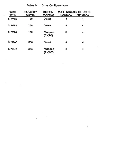
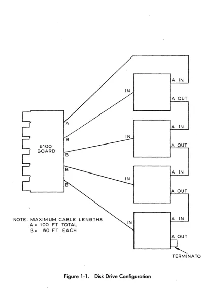
The disk drive interface conforms to standard flat cable specifications for SMD drives of Control Data Corporation and System Industries. The 519775 drive may emulate two 9766 drives and the 51 9784 may emulate two SI 97 62 drives~ Table 1-1 lists the drive configurations supported. Figure 1-1 illustrates the disk/controller cabling. Figure 1-2 illustrates cabling for dual port configurations.
Table 1·1 Drive Configurations
DRIVE CAPACITY DIRECT/ MAX. NUMBER OF UNITS
TYPE MBYTE MAPPED LOGICAL PHYSICAL
519762 80 Direct 4 4
51 9784 160 Direct 4 4
519784 160 Mapped 8 4
(2X80)
519766 300 Direct 4 4
51 9775 675 Mapped 8 4
(2 X 3(0)
[image:12.615.133.531.185.709.2]6100 USER'S GUIDE
6100 BOARD
NOTE: MAXIM UM CABLE LENGTHS A = 100 FT TOTAL
[image:13.620.90.486.83.648.2]B= 50 FT EACH
Figure 1-1. Disk Drive Configuration
PB61 00-9001-02
SYSTEM OVERVIEW
A IN
A OUT
A IN
A OUT
A IN
A OUT
A IN
A OUT
TERMINATOR
SYSTEM OVERVIEW
CPU
CPU
1-4
UNIBUS
UNIBUS
6100 BOARD
[image:14.612.100.480.221.502.2]6100 BOARD
Figure 1-2. Dual Port Configuration
6100 USER'S GUIDE
DUAL PORT DRIVE
,
6100 USER'S GUIDE PHYSICAL DESCRIPTION
2.0 PHYSICAL DESCRIPTION
The controller is a standard, 16 by 9-inch, single hex-slot board, incorporating a unique high-speed bipolar microprocessor design that exactly emulates the DEC PDP-11 RM02 Controller. The board
con-tains four 01 P switches used for such functions as device and vector addressing. The board also contains
one LED that is used for internal diagnostics. Refer to Section 4.0 for installation, cabling, and switch procedures.
2.1
Power Requirements
The following voltages are required to operate the controller.
+
5 Vdc ±5% @ 11 Amps Maximum-15 Vdc ±5% @ 0.7 Amps Maximum
2.2
Drive Interface
The disk drive interfaces to the controller board via two flat cables referred to as cables A and B.
2.2. 1 A-Cable
The A-cable is a 60-pin twisted pair flat cable that connects the first physical disk drive to the controller-board and is additionally used to daisy-chain disk drives.
2.2.2 I-Cable
The B-cable is a 26-pin ribbon flat cable that is radially connected from each disk drive to one of the four B-cable connectors on the controller board.
2.3
_Computer Interface
The following subsections describe the controller interface to the PDP-11 computer.
2.3. 1 UNIIUS Interface
The controller interfaces to the PDP-11 UNIBUS by plugging into any standard DEC Small Peripheral Controller (SPC) interface slot of the PDP-11 backplane.
,
2.3.2 Device, Interrupt, and Address Configuration Switches
Device, interrupt vector, and register group addresses are all switch selectable. By setting these switches the controller can be configured to allow for the emulation and mapping of several devices, the establishment of the device interrupt vector, and the starting address of the controller's control register group.
6100 USER'S GUIDE FUNCTIONAL DESCRIPTION
3.0 FUNCTIONAL DESCRIPTION
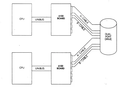
This section provides a brief description of the functional operation of the controller features. Figure 3-1 shows a simplified functional block diagram of the controller.
3. 1
Priority Levels
The controller's priority level is jumper selectable. Priority levels enable the controller to generate a processor interrupt request on one of the bus request levels, BR4 through BR7. Availability of the bus request is determined by receipt of a corresponding bus grant level, BG4 through BG7. Section 4.0 describes the priority level jumpering procedure. The controller is preset at a priority level of 5.
3.2
Overlapped Seeks
Overlapped seeks may be performed on all attached drives. This capability is provided by maintaining separate registers in the register file for each logical drive. Seeks are issued as they are received if a data transfer is not currently active on any drive. When a data transfer is in progress, a seek command to another drive is issued when the end of a cylinder is detected.
3.3
Dual Port Drive Compatibility
The controller can support dual port drives. This support is designed to be software transparent.
3.4
Contiguous Transfers
Contiguous transfers of sector data allow up to 64K bytes to be transferred in response to a single drive command.
3.5
RPS Look-Ahead
The RPS feature is compatible with DEC's look-ahead feature. The controller maintains a current sector count for each disk drive attached to it, this feature provides the programmer with a means of optimizing disk accesses by minimizing rotational delay.
3.6
Search Command,_
The search command is compatible with the DEC RMOX search, and combines a seek with a search for the desired sector. This feature is used by the software to synchronize the disk rotational positioning with the issuing of data transfer commands.
3.7
Error Correction
Burst and data error correction is accomplished by the use of the AMD Z8065 Burst Error Processor (BEP). The BEP detects all errors and allows for correction of error bursts up to 11 bits in length. The error information is loaded into the ECC registers (RMEC1 and RMEC2) and the correction can be made by the system software.
""0 aJ 0-o o I -0 o o
...
I o 1'1.) CPUPROGRAM CONTFn. AND INSTRUCTION
REGISTERS
COMMON BUS
PROGRAM ADDRESS
INTERRUPTS
(SIMPLIFIED VERSION)
Figure 3-1. 6100 Block Diagram
D HOLDING REGISTER 4 SECTOR BUFFER STORAGE MODULE
r - - - , ! DRIVE
. " C Z
q
o
z
[image:18.797.97.741.68.552.2]6100 USER'SGUIDE FUNCTIONAL DESCRIPTION
An uncorrectable error is defined as any error field larger than the 11-bit burst. If an uncorrectable error is detected, a bit is set in the error register (RMER1) and the data transfer operation is aborted. The maximum delay time for correctable data errors is 2 milliseconds.
The controller's attempt to correct a burst data error is transparent to the operating system when the ECC switch (location 5L, switch 2) is set. Refer to Section 4.2.4 for a description of these switch settings.
3.8 Controller Registers
The controller communicates with the system's disk driver program via 19 registers located on the con-troller. The contents of these registers may be accessed by their UN I BUS address. A detailed description of the controller registers is contained in Appendix A and a register summary is contained in Appendix 8. The registers and their UNIBUS addresses are shown in Table 3-l.
Table 3-1 Registers and UNIBUS Addresses
Register UNIBUS Address
RMCS1 (Control and Status 1) 776700
RMWC (W ord Count) 776702
RMBA (UNIBUS Address) 776704 RMDA (Disk Address) 776706 RMCS2 (Control and Stc;Jtus 2) 776710 RMDS (Drive Status) 776712
RMER1 (Error 1) 776714
RMAS (Attention Summary) 776716
RMLA (Look-Ahead) 776720
RMDB (Data Buffer) 776722 RMMR1 (Maintenance 1) 776724
RMDT (Drive Type) 776726
RMSN (Serial Number) 776730
RMOF (Offset) 776732
RMDC (Desired Cylinder) 776734
RMHR (Holding) 776736
RMMR2 (Maintenance 2) 776740
RMER2 (Error 2) 776742
RMEC1 (ECC Position) 776744 RMEC2 (ECC Pattern) 776746
[image:19.627.122.495.320.675.2]6100 USER'SGUIDE INSTALLATION
4.0 INSTALLATION
This section describes the procedures required to install, cable, and set the four DIP switches on the con-troller. This section also contains procedures that may be required for modification of the PDP-11 and SMD disk drives . .
. 4.1
Visual InspectionBefore attempting to install the controller board or perform 'cabling operations, a visual inspection of the controller board, cables, disk drives, and PDP-1 1 backplane must be performed to determine the following:
• All components on the controller board are in place, secure, and not cracked or
broken
• Pin connections for A- and B-cables are not bent or broken
• Any jumper wires installed on the board are connected properly and securely
• A- and B-cables are not bent or cut, and pin receptacles are secure
• Disk drive(s) is (are) configured for 32 sectors
• Terminators are removed from all but the last disk drive
• Index and sector jumpers are set for B-cable
• Bus grant continuity jumper board is removed from the controller SPC slot
4.2
Switch Settings
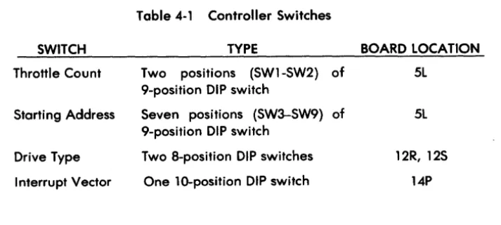
The controller board has four DIP switches that must be checked and/or set to conform to specific
in-stallation requirements. The switch locations on the board are shown in Figure 4-1 . Table 4-1 lists the
[image:21.621.133.490.495.655.2]switch name and type.
Table 4-1 Controller Switches
SWITCH TYPE BOARD LOCATION
Throttle Count Two positions (SW1-SW2) of 5L
9-position DIP switch
Starting Address Seven positions (SW3-SW9) of 5L
9-position DIP switch
Drive Type Two 8-position DIP switches 12R, 12S
Interrupt Vector One lO-position DIP switch 14P
LED A B C 0 E H J K L M N P Fl S
b
¢. "
I
o:J 0..
0 0 I
-0 0 0 --' I 0 t-..) 5L lo:::_~:--:mAOOR/THROTTLE Q
Figure 4-1 . Controller Switches
14P
12R P::~=~-_-:.-JI INTERRuPT
E]}
VECTORb:~~~~~-m
DRIVE CONFIGURATION 125~ !2
---r l f l l " _ _ - - '
[image:22.800.162.680.126.497.2]6100 USER'S GUIDE INSTALLATION
4.2. 1 DMA Throttle Count Switch
The throttle count switch determines how many words of data the controller will transfer, per
NP
re-quest, onto the UNIBUS. The throttle count only uses switches 1 and 2 of the 9-position DIP switch at grid location 5L. Table 4-2 shows the throttle count switch settings.SW1
OFF
OFF
ON
ON
Table 4-2 Throttle Count Switch Settings
SW2
OFF
ON
OFF
ON
DESCRIPTION
Throttle burst rate of 2 words per NP request. Simulates SACK.
Throttle at microprogram control.
Throttle at burst rate until SACK. If a higher priority request is received, the controller relinquishes the bus and asserts NPR.
Invalid setting.
Switch ON=O=closed Switch OFF = 1 =open
4.2.2 Register Set Address Switch (CS 1 )
The register set address switch determines the starting address of the controller register group. The register set address switch uses switches 3 through 9 of the same DIP switch used for the throttle count switch. Table 4-3 describes the standard switch settings for normal operation.
Table 4-3 Register Set Address Switch Settings
REGISTER SET 12 11 10 09 08
STARTING ADDRESS SW3 SW4 SW5 SW6 SW7
776700 OFF OFF OFF ON OFF
OR
776300 OFF OFF OFF ON ON
NOTE: Selectable address range ;s 760000 to 777700
Switch ON=O=closed Switch OFF = 1 =open
*UNIBUS address
PB61 00-9001-02
07 06*
SW8 SW9
OFF OFF
OFF OFF
[image:23.612.128.472.193.360.2] [image:23.612.138.485.483.562.2]I NST ALLA liON 6100 USER'S GUIDE
4.2.3 Drive Type Switches
Two 8-position 01 P switches (at. grid locations 12 Rand 12S) are used to determine the drive type
emula-tion and mapping. Table 4-4 illustrates which switches correspond to which physical drive numbers, and Table 4-5 illustrates the drive types configured by those switches. Each of the four drive type switch set-tings is polled, regardless of whether or not a physical drive is attached.
NOTE
[image:24.612.97.520.206.630.2]In a mapped or combined configuration, the logical drive numbers of some drives will not be the same as their physical drive numbers.
Table .4-.4 Drive Switches
DRIVE NO. SWITCHES
0 12R 5-8
1 12R 1-.4
2 .125 5-8
3 125 1-.4
Table .4-5 Drive Type Switch Settings
SWITCH
8 7 6 5
.4 3 2 EMULATION/ MAPPING
OFF ON ON ON RM03 80 Direct
OFF ON ON OFF RM03 160 Mapped
OFF ON, OFF ON RM03 160 Direct
OFF ON OFF OFF RM03 300 Direct
OFF OFF ON ON RM03 675 Mapped
ON OM, ON ON RM05 80 Direct
ON ON ON OFF RM05 160 Mapped
ON ON OFF ON RM05 160 Direct
ON ON OFF OFF RM05 300 Direct
ON OFF ON ON RM05 675 Mapped
NOTE: All other codes are reserved.
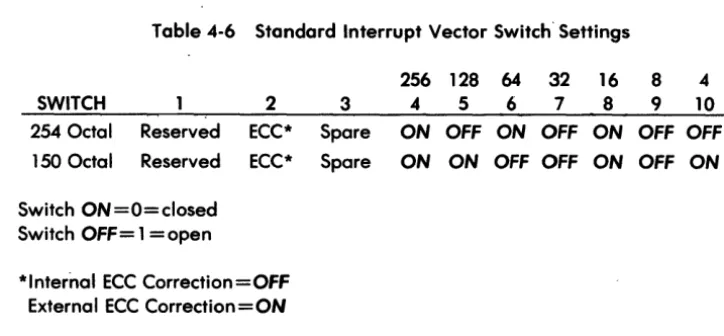
4.2.4 Interrupt Vector Switch
The interrupt vector switch is a 10-position DIP switch (located at grid location 14P) that sets the 3-digit octal word of the interrupt vector location. The standard interrupt vector location is 254 octal. Other disk interrupt vectors are defined in the DEC PDP-11 Peripherals Handbook. Table 4-6 shows the switch setting for the standard and alternate interrupt vectors.
6100 USER'S GUIDE INSTAllATION
Table 4-6 Standard Interrupt Vector Switch' Settings
256 128 64 32 16 8 4
SWITCH 2 3 4 5 6 7 8 9 10
254 Octal Reserved ECC* Spare ON OFF ON OFF ON OFF OFF
150 Octal Reserved ECC* Spare ON ON OFF OFF ON OFF ON
Switch ON=O=closed
Switch OFF = 1 = open
*Internal ECC Correction=OFF External ECC Correction=ON
4.3
Installation of the Controller BoardThe controller board can be installed in any PDP-11 Small Peripheral Controller (SPC) backplane hex slot. The following procedures should be followed to ensure proper installation.
CAUTION
Be sure to power down the system before con-tinuing with the installation procedure.
4.3.1
Index and Sector JumpersThe controller is normally configured to receive index/sector signals on the B-cable. For convenience under unusual circumstances, one (1) drive, and only one, can be allowed to transmit index/sector signals, via J-1 on the A-cable. In this case, that drive's B-cable must be connected to J-2 for proper controller operation. Additional drives whose B-cables are connected to J-3, J-4, or J-5 must have index/sector signals transmitted on their respective B-cables. The jumpers which allow index/sector selection between J-1 and J-2 are labeled W1 and W2 for J-2 and W3 and W 4 for J-1. The jumpers will be either in W1, W2 or in W3, W4, but not both. They are located at 5H. See Figure 4-2.
4.3.2
Priority Jumper.Before physically installing the controller board, determine the priority level to be established. The con-troller board's standard priority level is set at 5. This priority level is etched on the PCB board (BR5 and BG5) at the factory . To change the priority level, the preset board etches must be cut and jumper wires installed (e.g., to change to a setting of BG4 from a setting of BG5, cut etches at W5-F, W6-l, and E-K, and add jumpers at W5-E, W6-K, and F-l). Refer to Table 4-7 for BR-BG priority jumper settings. Refer to Figure 4-2 for an illustration of jumper installation.
[image:25.618.110.472.100.268.2]~ I 0-. I o t-..)
5H
A•
( o (W2
W
...
(SJ
,
,flJ
'~
~
, ,
o
)s]
W1
W3
DETAIL B
DETAIL A
~
J1 (A CABLE)
J2 (B CABLE)
r---,
.
.
I I I I.
t ______ , ____ :
"-SEE OETAL A
W1
OUT
[image:26.792.53.713.40.555.2]TN
Figure 4-2. Priority Jumpers
W2
OUT
lN
W3 W·4
,IN
IN'
OUT
'OUT
6100 USER'S GUIDE INSTALLATION
Table 4-7 Priority Jumper Settings
LEVEL JUMPER LOCATIONS
BR4 W7-A
BRS* W7-B
BR6 W7-C
BR7 W7-0
BG4 WS-E W6-K F-L H-M J-N
BGS* WS-F W6-L E-K H-M J-N
BG6 WS-H W6-M F-L E-K J-N
BG7 WS-J W6-N F-L E-K H-M
*BRS - BGS is standard feature and etched on PCB.
4.3.3 Nonprocessor Grant (NPG) Jumpers
The N PG IN signal on the wirewrap side of the PDP-11 backplane and the N PG OUT signal must not be
jumpered together in the slot occupied by the controller board. Normally PDP-11 backplanes come
with jumper wires installed. Similarly, all other NPG IN and NPG OUT pins must be connected through
wire jumpers in all empty SPC slots. Figure 4-3 shows the pin location for the wirewrap side of the backplane.
When a DMA device (e.g., the 6100 Controller) is installed in an SPC slot of a backplane (type DD11-B or later), the wire from COlA 1 to COl B1 must be removed from the slot.
4.4
Physical Installation
of Controller BoardBefore the controller board can be placed in the SPC slot, it may be necessary. to remove the small board (bus grant continuity jumper board) in the slot. When all the foregoing procedures have been completed, the board may be physically installed. The board can be placed in any available SPC slot. The board is installed by pressing it firmly into the selected SPC slot with the component side facing in the same direction as the components on the other boards.
4.5 Drive Sector Count
The controller requires that the drives be set up for 32 sectors. Refer to the System Industries Disk Drive User's Guide for drives sector information.
4.6 Index and Sector Signal Configuration
The controller requires the continuous presence of drive index/sector signals on the B-Cable. Refer to the System Industries Disk Drive User's Guide for correct drive configuration for continuous (nongated) index/sector signals on the B-Cable.
[image:27.618.125.429.76.281.2]I NST ALLATION
TOP
01 02 03 04 05 06 07 08 09
SLOT NO.
ROW A
B
C
D
E
F
6100 USER'S GUIDE
~LEWIRMAAP
SIDE SIDE
1 2
AOS'b
0 0 CO DO 0 0EO FO 0 0
HO J 0 0 Q
KO LO 0 0
MO NO 0 -0 po RO 0
0
SOTO 0 0
UOVO 0 0
NOTE:
IN THIS EXAMPLE THE JUMPER EXTENDS FROM GRID POSITIONS C09A1 TO C0981.
C 0 9 A 1
/ \ / \
\
ROW SLOT
NO. PIN SIDE
C 0 9 B 1 TO
/ V \ \
ROW SLOT PIN SIDE NO.
Figure 4-3. NPG Jumper Location
[image:28.613.74.533.93.671.2]I NST AllATION 6100 USER'S GUIDE
4.7 Disk Drive Cabling·
Disk drives must be cabled correctly to insure proper transfer and retrieval of data. Figure 4-4 illustrates the correct placement of the A- and B-cables on the controller board. This subsection details the pro-cedures necessary to connect System Industries drives in a daisy-chain configuration.
NOTE
When installing the cables, take care to ensure that pin one (1) on the controller is aligned through the cable(s) to pin one (1) on the drive(s).
In a daisy-chain configuration, each drive communicates to the controller throu~h a discrete B-cable
and a common A-cable. The A-cable is attached to connector J1. The free end e"f this cable is then
attached to the first drive in the daisy-chain. One is connected between connec;tor J2 on the controller board and the first drive in the daisy-chain. Additional B-cables are attached to the controller on con-nectors J3 through J5. The drive connected to J2 is designated as drive 0 and drives connected to J3 through J5 are designated as drives 1 through 3 respectively. The free end of each cable is attached to
the disk drive as specified for each drive type. '
NOTE
The total A-cable length must not· exceed 100 feet and the maximum length of each B-cable
must not exceed 50 feet.
Refer to System Industries Disk Drive User's Guide for cabling information for specific System Industries drives.
4.8 Power-Up
The system is now ready to be powered up. Refer to the PDP-11 Processor and System Industries Disk Drive manuals for exact power-up procedures.
INSTALLATION
4-10
PORT 3 B·CABLE
[image:30.637.95.524.209.557.2]PORT 2 B·CABLE
Figure 4-4. Controller Cable Placement
6100 USER'S GUIDE
~-+---A·CABLE
PORTO B·CABLE
PORT 1 B·CABlE
6100 USER'S GUIDE DIAGNOSTICS
5.0
DIAGNOSTICS
The controller has internal diagnostics that are compatible with the DEC diagnostics listed in this section.
5.1
Internal Diagnostics
The controller contains in-PROM internal diagnostics. After power-up, the controller performs the following diagnostic tests:
1. Microprocessor self-test 2. Data RAM test
3. Register file test
During testing, the LED on the controller board is on. If the diagnostic tests indicate no failures, the con-troller turns the LED off. If there is a failure, the LED remains on, indicating a concon-troller error.
5.2
System Industries Disk Exerciser
The System Industries disk exerciser program is EXOR11. This program is on a magnetic tape and is pro-vided by System Industries with every 6100 Controller. When the program is loaded on the system, the title
TITLE JIMZAP - DISC EXERCISER V1.6
EXOR11 6 - AUG - 1981
appears followed by the first program prompt. Possible prompts and responses are described in this section. The operator responds to the prompts by entering an octal number followed by a carriage return.
PROMPT FILL COUNT
STATUS
VECTOR
ENTER TEST TO BE RUN
ENTER PATTERN NUMBER
PB61 00-9001-02
RESPONSE
10 for CRT, 0 or 2 for teletype (default is 4)
Beginning address of status registers (default is 176700)
Interrupt vector number (default is 254)
There are seven tests: bit 0
=
formatbit 1
=
read entire disk bit 2 = read/writebit 3 = random read/write bit 4 = seek
bit 5 = interrupt
all tests = 77 {default is all tests}
This prompt is printed only when read/write test is selected. There are five patterns:
o
= address of buffer location1
=
1333332
=
1252523
=
1777774 = 00000o (default is 0)
DIAGNOSTICS 6100 USER'SGUIDE
PROMPT
ENTER RUN PARAMETERS
ENTER NUMBER OF CYLINDERS
ENTER STARTING CYLINDER
DISKS TO TEST
RESPONSE
The run parameters are: bit 0
=
short passbit 1 = do not type errors bit 2
=
format every pass bit 3 = halt on error bit 4=
loop on errorbit 5 = do not type test names, or pass numbers bit 6
=
timeout switch(default is 0, format first pass and test all cylinders)
This prompt is printed only when short pass is selected. Enter number of cylinders to test. (NO DEFAULT)
This prompt is only printed when short pass is selected. Enter starting cylinder number. (NO DEFAULT)
There are seven possible units, enter the value number:
Unit # Bit # Value
0 0 1
1 1 2
2 2 4
3 3 10
4 4 20
5 5 40
6 6 100
7 7 200
(NO DEFAULT)
The operator always has control of the CPU from the console. The following commands are available.
5-2
CTRL B
=
Boot (for boot options type "?") CTRl C=
Restart at level 0CTRl 0
=
Restart at level 0 CTRL E=
Restart at level 2CTRL F
=
Print cylinder, head, and sector CTRL H=
Toggle halt on errorCTRL L
=
Toggle loop on error CTRL N=
Print current ECIBCTRL 0
=
Toggle print error messages CTRl P=
Print the ECIB table6100 USER'S GUIDE
CTRL Q = Proceed
CTRL R = Restart with same arguments CTRL S = Halt
CTRL T
=
Toggle timeout flagCTRL U
=
Toggle print pass number+
test titles CTRL X=
Print all registersRESTART ADDRESSES
1600
=
Same as CTRL C 1604=
Same as CTRL R 1610=
Same as CTRL B5.3 DEC Diagnostics
DIAGNOSTICS
The controller is compatible with the following DEC formatters and diagnostics for 80 and 160 Mbyte (mapped) drives without modification:
PROGRAM NAME EMULATION DESCRIPTION --"---CZRMACO RM03/RM02 Formatter
CZRMBBO RM03/RM02 Performance Exerciser CZRMECO RM03/RM02 Functional Test 3, 2 CZRMFBO RM03/RM02 Extended Drive Test CZRMIBO RM03/RM02 Drive Compatibility Test
The controller is compatible with the CZRMCB2 Functional Test 1 for RM03/RM02 with the following changes:
TEST LOCATION IS CHANGE TO
11 12036 4 137
12040 240 13110
36 24212 4 137
24214 240 24n6
41 26600 1007 407
53 32260 4 137
32262 240 32646
61 35570 1406 406
64 37002 4 137
37004 240 37362
6100 USER'S GUIDE INSTRUCTIONS AND REGISTERS
APPENDIX A
A register bit followed by an asterisk indicates a bit whose function differs from DEC definitions. Registers are referred to by their name and UN I BUS address.
Control and Status 1 Register (RMCS 1) (776700)
RMCS1 register is used to store the current disk command function code and operational status of the
controller. '
15 I SC
Bit 15 14 13* 12 11* 10* 09-08 07
14 13 12 11
I TRE MCPE
tIi~:I~:~:~:1
OVAName
Special condition (SC)
Transfer error (TRE)
MASSBUS control bus parity error (MCPE)
Not used
10 09
IpSEl IA17
Type
Read only
Read/write
Read only
Drive available Read only
(DVA)
Port select (PSEL) Read/write
A17-A16 UNIBUS Read/write
address extension bits
Ready (RDY) Read only
MASSBUS is a trademark of Digital Equipment Corporation.
PB61 00-9001-02
08
I A1
07 06 05 04 03 02 01 00
I ROY I IE I F4 F3 F2 F1 FO
I
GOI
Function
Set when TRE or any drive ATA bit is set. Cleared by clearing the TRE or ATA conditions.
Set when one or more RMCS2 bits (08-15) are set, or a drive error occurs during a data transfer. Cleared by UNIBUS INIT, controller clear, loading a data transfer command with GO bit set, or by writing a 1 to this bit causing an error clear.
Set to 0 by controller.
Always read as O.
Set to 1 by controller.
Read/write for diagnostic purposes and has no effect on controller operation. Cleared by UNIBUS INIT, controller clear, or by writing a 0 in this bit.
Upper extension bits of the RMBA register. Cleared by UNIBUS INIT, controller clear, or by writing 0 in these bit positions. Cannot be' modified while con-troller is performing a data transfer.
RDY normally = 1. During data transfers,
RDY =
o.
When a data transfer command code(51-73) is written into RMCD1, RDY is reset. At the termination of the data transfer, RDY is set.
INSTRUCTIONS AND REGISTERS
RMCS 1 (continued)
Bits
Name06 Interrupt enable
(IE)
Type
Read/write
6100 USER'S GUIDE
Function
I E is a control bit that can be set only under pro-gram control and enables an interrupt to occur when the following conditions are satisfied.
1. Upon termination of a data transfer if IE is set when ROY becomes asserted.
2. If SC, IE, and ROY are
011
asserted.3. If the program writes a 1 into IE and ROY at the same time.
Cleared by UNIBUS INIT, controller clear, or automatically cleared when an interrupt is recognized by the CPU. When a 0 is written into IE by the program, any pending interrupts are cancelled.
05-01 00
F4-FO and GO bit. Read/write F4-FO and the GO bit (00) ore function (command)
code control bits.
F4 F3 F2 Fl
o
0 0 00 0 0 1
0 0 0 1 0 0 0 0 0 0 0 0 0
o
0 1o
0 1 10 0 0 0 0 0
o
0
1 0 0
1 0 1 0
1 0 0 1 0 0
1 1 0
1 0
FO GO Octal
o
1 01o
1 051 1 07
o
1 11o
111 13
o
1 151 1 17
o
1 211 1 23
o
1 31o
1 511 53
o
611 63
o
711 73
No operation Seek command Recalibrate Drive clear Drive clear
Release (dual sort operation) Offset command
Return to centerline Read-in preset
Pack acknowl~dge
Search command Write check data
Write check header and data Write data
Write header and dato Read data
Read header and data
The GO bit (RPCS1, bit 0) must be set to cause the controller to respond to a command. The GO bit is reset by the controller after command execution.
6100 USER'SGUIDE INSTRUCTIONS AND REGISTERS
Word Count Register (RMWC) (776702)
RMWC is the word count register. It is loaded by the program with the two's complement of the number of words to be transferred. During a data transfer, it is incremented by 1 each time a word is transmitted to or from memory. A maximum of 65,535 words can be transferred at one time.
15 14 13 12 11 10 09 08 07 06 05 04 03 02 01 00
I~I~I~I~I~I~I~I~I~I~I~I~I~I~I~I~I
Bit Name Type
15-00 Word count (WC) Read/write
Function
Set by the program to specify the number of words to be transferred (two's complement form). Cleared only by writing zeros into all bits. RMWC is updated by the controller at the end of each complete sector transferred, or after each word of a sector of less than 256 words.
UNIBUS Address Register (RMBA) (776704)
RMBA register is used to address the memory location in which a transfer is to take place. The RMBA register forms the lower 16 bits of the address that combine with bit-09 and bit-08 of the control register RMCS1 to create the 18-bit memory address. The register is loaded with the starting memory address by the program. Each time a DMA transfer is made, the register is incremented by 2. If the BAI (bus address increment inhibit) bit (bit-03 of RMCS2) is set, the incrementing of the register is inhibited and all transfers take place to or from the starting memory address.
15
I
SA 1Bit 15-01
o
14 13 12 11
SA 1 SA 1 SA 1 SA
Name
UNIBUS address (BA)
Not used
PB61 00-9001-02
10 09
1 SA 1 SA
Type Read/write
08
1 SA
---
---07 06 05 04 03 02 01 00
1 SA 1 SA 1 BA
I
SA 1 SA I- SA SAl~j~jIi1I~1
Function
Loaded by the program to specify the memory address of a transfer. Cleared by UNIBUS INIT, or by controller clear. The RMBA register is incremented by 2 after each transfer of a word to or from memory.
Always read as O.
INSTRUCTIONS AND REGISTERS 6100 USER'S GUIDE
Disk Address Register (RMDA) (776706)
RMDA register is used to address the sector and track on the disk to or from which a transfer is desired. The RMDA register is associated with the drive whose unit number appears in bits 00-02 of the status register RMCS2. Before a transfer, the RMDA register is loaded by the program with the address of the first block to be transferred. RMDA is incremented each time a block of data has been transferred so that consecutive blocks are automatically addressed when the word count indicates that more than one block is to be transferred.
15
14
13
12
1110
09 0807
0605
0403
02
01
001!!!!!!!j!!!!!!!!!!!f!!!!!!!!!Jj!!~!!!!!!!f!!!!!!!!d!!!!!!!!!!h
A
16
ITA8
ITA4
IT
A2 ITA 1
1i!!!~!!aI!!i!!!l!!!i!!!&!!!!!!!i!!!H!!!!!!~E!!!!!IlsA
16
ISA8
ISA4
ISA2
ISA 1
I
Bit
15-13
12-08
07-05
04-00
A-4
Name Not used
Track address (TA)
Not used
Sector address (SA)
Type
Read/write
Read/write
Read/write
Read/write
Function
Set by the program to specify the track on which a transfer is to start. Cleared by read-in pr"eset com-mand. Updated by controller at the end of each sector.
Set by the program to specify the sector on which a transfer is to start. Cleared by read-in preset com-mand. Updated by controller at the end of each sector.
6100 USER'S GUIDE INSTRUCTIONS AND REGISTERS
Control and Status 2 Register (RMCS2) (776710)
RMCS2 register indicates the- status of the controller and contains the drive unit number. The unit number specified in bits 00-02 of this register indicates which of the possible 4 physical or 8 logical drives is selected.
15 14 13 12 11 10 09 08 07 06 05 04 03 02 01 00
IOlT IWCE I UPE I NED INEM I PGE IMXF b\OPE lOR I IR I ClR I PAT I BAI I U2 U1 UO
Bit Name T~~. Function
15* Data late (DLT) Read only Set to 0 by controller.
14 Write check error Read only Set when the controller is performing a write/check
(WCE) operation and a word on the disk does not match
the corresponding word in memory. Cleared by UNIBUS INIT, controller clear, error clear, or loading a data transfer command with GO bit set.
WCE causes TRE to be set. If a mismatch is detected during a write-check command execution, the transfer terminates and the WCR bit is set. The memory address displayed in RPBA (and extension) is the address of the word following the one that did not match (if BAI is not set). The mismatched data word from the disk is displayed in the data buffer (RPDB).
13 Parity error (U PEl Read/write Set if a UNIBUS parity error is detected during a
write or write-check command. This bit may be set and cleared for diagnostic purposes by writing to it. Cleared by UNIBUS INIT, controller clear, error clear, or loading a data transfer command with GO bit set.
12 Nonexistent drive Read only Set when the program reads or writes a register
(NED) associated with a drive that does not exist, or is
powered down. Cleared by UNIBUS INIT, con-troller clear, error clear, or loading a data transfer command with GO bit set. NED sets TRE.
INSTRUCTIONS AND REGISTERS
RMCS2
(continued)Bit
11 10 09 08* 07 06* 05 A-6 Name Nonexistent memory (NEM)Program error (PGE)
Missed transfer (MXF)
Type
Read only
Read only
Read/write
MASSBUS data bus Read only parity error
(MDPE)
Output ready (OR)
Input ready (IR)
Controller clear (CLR)
Read only
Read only
Write only
6100 USER'SGUIDE
Function
Set when the controller is performing a DMA transfer and the memory address specified in RPBA is nonexistent (does not respond to MSYN within 10 microseconds. Cleared by UNIBUS INIT, controller clear, error clear, or loading a data transfer com-mand with GO bit set. NEM sets TRE. The RPBA contains the address+ 2 of the memory location causing the error.
Set when the program attempts to initiate a data transfer operation while the controller is currently performing one. Cleared by 'UNIBUS INIT, con-troller clear, error clear, or loading a data transfer command with GO bit set. PGE sets TRE. The data transfer command code is inhibited from being written.
Set if a data transfer command is loaded with ERR set in RMDS, or if DMA transfers between the UNIBUS and the controller's data buffer fail to complete. This bit may be set or cleared for diagnostic purposes by writing to it. Cleared by UNIBUS INIT, controller clear, error clear, or loading a data transfer command with GO bit set. MXF sets TRE.
Set to 0 by controller.
Set by controller to indicate a word is in RPDB.
Set to 1 by controller.
When a 1 is written into CLR bit, the controller and all drives are i.nitialized. The following controller bits are cleared: RMCS1 bits 6, 8-10, 13-15, RMCS2 bits 0-5, 7-15, and RMBA. The following drive bits are cleared: RMER1, RMER2, RMCS1 bits 0-5, RMAS, RMEC2, and RMDS bits 14-15. A UNIBUS INIT command also causes controller clear to occur.
6100 USER'S GUIDE
RMCS2
(continued)Bit Name
04* Parity test (PAT)
03 UNIBUS address increment inhibit (BAI)
02-00 Unit select (U2-UO)
PB6100-9001-02
Type Read/write
Read/write
Read/write
INSTRUCTIONS AND REGISTERS
Function
PAT bit has no effect on 6100 operation. Cleared by UNIBUS INIT or controller clear.
When BAI is set, the controller will not increment the RMBA register during a data transfer. BAI bit cannot be modified while the controller is doing a data transfer (ROY negated).
U2-UO bits are written by the program to select a drive.
Cleared by UNIBUS INIT or controller clear.
The unit select bits can be changed by the program during data transfer operations without interfering with the transfer.
INSTRUCTIONS AND REGISTERS 6100 USER'SGUIDE
Drive Status Register (RMDS) (776712)
RMDS contains status indicators for the selected drive. The status indicators displayed are those of the drive that is specified by the unit select bits (OO-02) of the RMCS2 register.
15 14 13 12 11 10 09 08 07 06 05 04 03 02 01 00
I
AT AI
ERRI
PIPI
MOL I WRl IlBT I PGMI
DPR I DRY Iw
1~~~tij~~~~~~~~~~l~t~.~~I~~~~~f~~~~~~~~ij~~I~~j~~~J~~~I~bt~~~t~iI~~]~t~~j~I~1
OMI
Bit 15 14 13 12
A-a
NameAttention active (ATA)
Error (ERR)
Positioning in progress (PI P)
Medium on-line (MOL)
Type
Read only
Read only
Read only
Read only
Function
An attention condition from a drive will set the AT A bit and the corresponding AT A summary bit in RPAS.
ATA is cleared by UNIBUS INIT, controller clear, loading a command with the GO bit set, or, if no error conditions exists, writing a 1 in the RPAS register bit corresponding to the drive's unit number.
An attention condition is caused by:
1. any error in the error registers if
a. GO bit set at completion of command,
b. GO bit reset at occurrence of error
2. at completion of seek, search, recalibrate, offset or return to centerline
3. MOL changes state.
Set when either of the error registers RMER1 or RMER2 indicates a drive error. Cleared by UNIBUS INIT, controller clear, drive clear, or by writing 0 in error registers.
Set by drive when a positioning command is accepted. These commands are seek, offset, recalibrate, and search. The PIP bit is also set during implied seeks, mid-transfer seeks, and offset operations during a read. The bit is cleared when the function is completed.
Set for the drive upon the successful completion of the start-up cycle. Cleared when the drive is spun down or switched off. (This bit is set when unit-ready from the drive is asserted and cleared when it is d~asserted.)
6100 USER'SGUIDE
RMDS
(continued)Bit Name
Type
11 Write lock (WRl) , Read only
10 last block Read only
09* Programmable Read only
(PGM)
08* Drive present Read only
(DPR)
07 Drive read (DRY) Read only
06 Volume valid (W) Read only
05-01
00
Not used
Offset mode (OM) Read only
PB61 00-9001-02
INSTRUCTIONS AND REGISTERS
Function
Set when last addressable sector on the disk pack has been tried or written.
Set when last addressable sector on the disk pack has been read or written.
Set to 0 by controller.
Set to 1 by controller.
Set at the completion of every command, data handling or mechanical motion.
Cleared at the initiation of a command.
If this bit is reset, the controller cannot issue another command. When set, this bit indicates the readiness of the drive to accept a new command.
DRY is the complement of the GO bit except when the drive is nonexistent; then DRY is reset.
Set by the pack acknowledge or read-in preset command.
Cleared whenever drive cycles up from the OFF state and on controller power-up.
When reset,
W
bit indicates drive went off-linethen on-line, and a possible disk pack change.
Always read as O.
Set when offset command is issued to drive. When set, and a read command is received, the offset is performed prior to the execution of the read.
Reset by any of the following actions: 1. Power-up
2. Mid-transfer seek 3. Read-in preset
4.
Write data or write header and data5. Return to centerline 6. Write cylinder desired 7. Recalibrate
INSTRUCTIONS AND REGISTERS 6100 USER'SGUIDE
Error Register #1 (RMER1) (776714)
RMER 1 contains the error status indicators for the drive whose unit number appears in bits 00-02 of the RMCS2 register. The logical OR of all the error bits in the RMER1 and RMER registers are written into bit 14 of the RMDS register.
Errors can be classified into two categories: Class A and Class B.
• Class A errors are handled at the completion of a non-data transfer command, or in the case of a data transfer command, at a sector boundary provided the run line is inactive.
• Class B errors cause the command to terminate immediately, or as soon as possible.
15 14 13 12 11 10 09 08 07 06 05 04 03 02 01 00
lOCK
I
UNSI
OPI forE f WlE IIAE I AOE~CRC
I HCE I ECH IWCF I FER I PAR I RMR IllR I IlFI
Bit Name T~~e Function
15 Data check (DCK) Read/write Set during a read operation when the ECC
hard-ware has detected an ECC error after the ECC bytes have been looked at.
Cleared by a drive clear command, UNIBUS INIT, controller clear, or by writing 0 into the register.
14 Unsafe (UNS) Read/write Set when bit 7 (DVC) of RMER2 is set.
Cleared by drive clear, UNIBUS INIT, or controller clear.
13 Operation Read/write Set if during a search or data transfer command the
incomplete (OPI) correct sector is not located.
12* Drive timing error Read/write Set to 0 by controller.
(DTE)
11 Write lock error Read/write Set when the program attempts to issue a write
(WLE) command to a drive that has write-protect switch
on.
Cleared by UNIBUS INIT, drive clear, controller dear, or by writing 0 into the register.
10 Invalid address Read/write Set when the address in the desired cylinder register
error (IAE) (RMDC) or the disk address register (RMDA) is
invalid and a seek, search or data transfer opera-tion is initiated.
6100 USER'S GU IDE
RMERl
(continued)Bit
09
08
07
Name Type
Address overflow Read/write
error (AOE)
Header CRC error Read/write
(HCRC)
Header compare error (HCE)
Read/write
PB61 00-9001-02
INSTRUCTIONS AND REGISTERS
Function
Set when the desired cylinder register (RMDC) overflows during a read or write.
Cleared by UNIBUS INIT, drive clear, controller clear, or by writing 0 into the register.
Setting of this bit indicates that the desired cylinder address register has exceeded the maximum cylinder address.
Set if bit 10 (HCI) of RMOF is not set and the con-troller detects a CRC error in the header.
Cleared by UNIBUS INIT, drive clear, controller clear or by writing 0 into the register.
Set if bit 10 (Hel) of RMOF is reset and one or more of the following occurs while reading the header:
1. Bits 00-09 of the first header word do not match bits 00-09 of the desired cylinder address register (RMDC).
2. Bits 10, 11, and 13 of the first header word are not zero.
3. Bits 00-15 of the second header word do not match bits 00-15 of the desired track/sector register (RMDA).
Cleared by UNIBUS INIT, drive clear, controller clear, or by writing 0 into the register.
NOTE: Bits 14 and 15 must be set in the first header word or BSE will be set. Also, bit 12 of the
first header word must be a 1 or FER will be set.
However, these ·errors do not set HCE.
INSTRUCTIONS AND REGISTERS 6100 USER'S GUIDE
RMER 1
(continued)Bit·
Name T~~eFunction
06 ECC hard error Read/write Set at the conclusion of the error correction
pro-(ECH) cedure (bit 15 (DCK) of this register set and bit 11
(ECI) of RMOF not set), indicating that the error was an uncorrectable ECC error.
Cleared by UNIBUS INIT, drive clear, controller clear, or by writing 0 into the register .
05* Write clock fail . Set to 0 by controller.
(WCF)
04 Format error Read/write Set when reading a sector header if bit 10 (HCI) of
(FER) RMOF is not set and bit 12 of the first header word
is not set to ali or if bit 12 of RMOF is not set to a 1 and a data transfer command is executed.
NOTE: The controller words are in 16-bit word length mode only.
Cleared by drive clear, controller clear, UNIBUS INIT, or bY,writing 0 into the register.
03* Parity error (PAR) Set to 0 by controller.
02 Register modifica- Read/write Set when a write is attempted to any drive register
tion refused (except RMAS) while the GO bit is set.
(RMR)
Cleared by UNIBUS INIT, controller clear, drive clear, or by writing 0 into the register.
01* Illegal register Set to 0 by controller.
(ILR)
00 Illegal function Read/write Set when the function code in the control register is
(ILF) illegal and the GO bit is set.
Cleared by UNIBUS INIT, drive clear, controller clear, or by writing 0 into the register.
6100 USER'SGUIDE INSTRUCTIONS AND REGISTERS
Attention Summary Register (RMAS) (776716)
RMAS allows the program to examine the attention status of all the drives with only one register read operation. It also provides the means for resetting the attention logic in a selected group of drives. The bit displayed in each of the eight low-order positions of this register is identical to the ATA bit displayed in the RMDS register for the corresponding drive. When fewer than four drives are attached to the
con-troller, the bits corresponding to the missing drives are always O.
15 14 13 12 11 10 09 08 07 06 05 04 03 02 01 00
1!!I!i1!1I!1!1iII!i.1IIH~~!~I~i~j~j~1~1~1¥~1Ii.!I~~~!~11!i!jl~II!1!~!~!l!~!ql~I!~~~~11I~~~ij~~~~~I~~!lI~!!!ijI~!~!~m
AT A I AT A lATA I AT A I AT A I AT A I AT A I AT AI
Bit 15-08
07-00
Name Not used
Attention active (ATA)
PB61 00-9001-02
Typ.
Read/write
Function
Read as O.
Each AT A bit is set when the corresponding drive asserts its A T A bit.
All bits are cleared by UNIBUS INIT or controller clear. Individual bits are cleared by loading a func-tion code with the GO bit set in the corresponding drive or by writing a 1 in the AT A bit positions of this register. Writing a 0 has no effect.
Each drive's AT A bit is displayed in bit 15 of R PDS. Each drive also responds in the bit position of RMAS register that corresponds to its unit number; e.g., drive 02 responds in bit position 02 of RMAS register.
INSTRUCTIONS AND REGISTERS 6100 USER'S GUIDE
Look-ahead Register (RMLA) (776720)
RMLA contains the count. of the sector that is currently positioned under the heads. The value is represented as a binary number in bit locations 06-10, where bit 6 is the LSB. The maximum count for a 16-bit/word format is 31 and for an 18-bit/word format is 29.
15
14' 13
12
11
10
09 0807
0605
04
03
02
01
00~~lI~li~I~~~~~III~i~1I~~iIIli~IIl~ilIIi~l~lI~l:l:llI:l:~i:Ilj]SC16
Isca
ISC4
ISC2
ISC1
Ij~jl~~jil:l~l:Il~lI:I:l:lI:l:[:l:j~l:l:Il~l:Il:li~:Il:l:tIl:l:lil:lI:l:lt:lllIlil:I:Ill
Bit Name Type
15-11 Not used
10-06 Sector count
(SC 1-16)
05-00 Not used
Data Buffer Register (RMDB) (776722)
Function
Read as O.
Set to correspond to the current sector count value. Reset by the index pulse.
Read as O.
RMDB is used to monitor the data buffer and provide the bad data word as a result of a bad data com-pare operation.
15
14
13
12
1110
09 0807
0605
0403
02
01
00I
DB I DB I DB I DB I DB I DB I DB I DB I DB DB I DB I DB I DB I DB I DB I DBBit Name Type Function
15-00· Data buffer (DB) Read/write Contains the bad data word as the result of a data
compare operation.
Maintenance Reglster,l (RMMR 1) (776724)
RMMR 1 is not emulated.
15
14
13
12
1110
09 0807
0605
04 0302
01
00Illl:llltilIJllillllllllli.:IlI:IIlIi.:l:IIiIlIi:IIl:l}IjdIl:l:l:!I:l:l:Iil:l~I!:I:l:l:!:i.l:!~l:l:l:l:l:l:l:i!llllIl[r~i:[:li:j:[~!:l:~:II!:]).:l:l:l:IJ~l:!:[:[i:!:!:l:l:l:!:!:N~:!:I[U:[:tll.:[:~~~Il:I~~~I.:I~:[:~lIII.:[I:[:ll~:I~tiI[~H
Bit Name Type Function
15-00 None Set to 0 by controller.
Figure


Related documents
The RTC8563 then begins to transmit data starting with the register address pointed to by the register pointer. If the register pointer is not written to b efore the initiation of
When assigning Special Tools to a part from Tool Inventory, any Special Tools from the Tool List which do not have an *.SPT file in the Special Tool folder are grayed-out..
youngsters and the women to buy scooters Major players in the 2- wheeler industry are Hero Honda Motors Ltd (HHML), Bajaj Auto Ltd (Bajaj Auto) and TVS Motor Company Ltd (TVS)..
Prior to arriving at Murray State, Bubb spent fi ve years at Idaho State University, fi rst serving as assistant athletic director for development (2003), and then senior
To the left is the original 18th century section of the property and the living room is at the front of the cottage with triple aspect windows looking out to the gardens..
this research is useful because implemented integrated wireless fault diagnosis system can be utilized with anther rotor machine for protecting or prevention the
© Annals of Translational Medicine All rights reserved Ann Transl Med 2016;4(22) 443atm amegroups com Page 1 of 11 Original Article During economic crisis can sleep questionnaires
FileStore allows you to store and access your MS Office™, scanned paper, email or any other documents from one, easy-to-use, web-based system.. It gives you a 360-degree view of all
