Advanced Scattering Techniques. (Under the direction of Jacob L. Jones).
Dielectric and ferroelectric materials are widely used in many applications, such as energy storage capacitors, actuators in micro-positioning devices, and ultrasound medical therapy devices. The demands of advanced materials with multi-functionalities, precise responses under different stimuli, or stable performance in harsh conditions, are growing nowadays. Usually such advanced materials have complex structures such as the deviation of local structure from long-range structures, non-equilibrium states, phase co-existence, and complicated microstructures. These complex structures result from a variety of reasons, e.g. the competing internal forces, flattened Gibbs free energy profiles, specific synthesis routes, etc. Since the dielectric and ferroelectric property of a material is a function of its structures, and the structures strongly depend on the processing methods, it is crucial to have a good understanding of the processing-structure-property relationships of these complex dielectrics and ferroelectrics. However, due to lack of sophisticated characterization techniques and data analysis methods, there are only limited studies on the comprehensive structural characterization of these complex materials.
The work in this dissertation characterizes the crystallographic structures of multiple complex dielectrics and ferroelectrics. These fundamentally important materials of interest are: lead-free ferroelectric Na1/2Bi1/2TiO3-xBaTiO3 (NBT-xBT), Si-doped HfO2 fluorite, spinel compound CoxMn3-xO4 (CMO), high temperature dielectric BaTiO3-xBi(Zn1/2Ti1/2)O3
To elucidate the role of processing factors on the structures of NBT-xBT, in situ XRD during reaction was conducted. A new formation mechanism is proposed. Studying the processing in situ helps in understanding the reaction sequences, also helps in designing new processing route.
The processing-structure relationship study of Si-doped HfO2 was conducted using high resolution XRD. The calcination temperature and SiO2 particle size play important roles in the incorporation of Si into HfO2 and the diffusion of Si out of (Hf,Si)O2 solid solution. The obtained (Hf,Si)O2 is confirmed as a non-equilibrium state. This work demonstrates that the processing conditions can be optimized to control the phases in Si-doped HfO2 final products. The structures of CMO ceramics are characterized using combined analysis of neutron and X-ray diffraction. A tetragonal to cubic spinel transition was observed by addition of Co on B-sites. The lattice parameters, phase fraction, and atom-atom bond lengths were obtained by Rietveld method. This study contributes to a more thorough understanding of the structures in CMO spinel oxides.
function of applied electric field were obtained, showing evidence of a field-induced phase transition and polarization rotation. In addition, the atomic-scale responses from local structure give more evidence of the polarization rotation mechanism in PMN-0.30PT ceramics.
by Dong Hou
A dissertation submitted to the Graduate Faculty of North Carolina State University
in partial fulfillment of the requirements for the degree of
Doctor of Philosophy
Materials Science and Engineering
Raleigh, North Carolina 2017
APPROVED BY:
_______________________________ _______________________________
Jacob L. Jones Elizabeth Dickey
Committee Chair
_______________________________ _______________________________
BIOGRAPHY
ACKNOWLEDGMENTS
I would like to thank my advisor Prof. Jacob L. Jones for his patient guidance, rich knowledge, and expertise in research. Also, I appreciate all the opportunities he offered for completing this work. I sincerely acknowledge the guidance from my committee members: Prof. Elizabeth Dickey, Prof. Veronica Augustyn, and Prof. Xiaoning Jiang.
I want to thank all the present and past members of Prof. Jacob L. Jones’ research group
for their company and support: Dr. Chris M. Fancher, Dr. Tedi-Marie Usher, Dr. Thanakorn Iamsasri, Dr. Stephen Podowitz-Thomas, Dr. Ching-Chang Chung, Dr. Deepika Saini, Dr. Giovanni Esteves, Jason Nikkel, Jonathon Guerrier, Brienne Johnson, Jianwei Zhao, and Hanhan Zhou.
I would like to thank all the collaborators from other universities and institutes: Prof. Takaaki Tsurumi, Prof. Hiroaki Takeda, and Prof. Takuya Hoshina from Tokyo Institute of Technology; Dr. Hana Ursic and Dr. Barbara Malic from Jozef Stefan Institute; Dr. Igor Levin from National Institute of Standards and Technology; Prof. David P. Cann from Oregon State University; Dr. Elena Aksel from SCHOTT AG, Germany; Dr. Lili Zhao from Northwest University, China; Dr. Sungwook Mhin from Korea Institute of Industrial Technology; and Dr. Jennifer S. Forrester from University of Leeds.
technical assistance of Kevin Beyer, Olaf Borkiewicz, Karena Chapman, Rick Spence, and Yang Ren at Sector 11 is gratefully acknowledged. A portion of this research used resources at Spallation Neutron Source, a DOE Office of Science User Facility operated by the Oak Ridge National Laboratory. The assistance from Dr. Ashfia Huq and Dr. Katharine Page at Spallation Neutron Source is acknowledged. I would like to thank the organizers of the 18th National School on Neutron and X-ray Scattering.
I acknowledge the financial support provided by my advisor and the China Scholarship Council. The neutron scattering research in Chapter 5 is supported by Korea Institute of Industrial Technology. The research in Chapter 6 is supported by U.S. Department of Commerce under award No. 70NANB13H197. The research in Chapter 7 and my visit to Jozef Stefan Institute is financial supported by Slovenian Research Agency under bilateral project: BI-US/15-16-60.
TABLE OF CONTENTS
LIST OF TABLES ... viii
LIST OF FIGURES ... ix
CHAPTER 1 Introduction and Background ... 1
1.1 Introduction ... 1
1.2 Properties of Complex Functional Ceramics ... 2
1.2.1 Dielectrics and Dielectricity ... 3
1.2.2 Piezoelectrics and Piezoelectricity ... 5
1.2.3 Ferroelectrics and Ferroelectricity ... 6
1.2.4 Relaxor Ferroelectrics ... 8
1.3 Crystal structures ... 10
1.3.1 Perovskites ... 11
1.3.2 Fluorites ... 16
1.3.3 Spinels ... 17
1.4 Ceramics Processing ... 18
1.5 Dissertation Overview ... 20
CHAPTER 2 Advanced Scattering Techniques and Data Analysis Methods ... 22
2.1 Background ... 22
2.2 Structural Characterization with Diffraction Techniques ... 23
2.2.1 Laboratory X-ray Diffraction ... 23
2.2.2 Synchrotron X-Ray Diffraction ... 24
2.2.3 Neutron Diffraction ... 25
2.2.4 In situ Diffraction Techniques ... 26
2.2.5 Analysis of Diffraction Data ... 27
2.3 Structural Characterization with Total Scattering Techniques ... 30
2.3.1 Pair Distribution Function... 31
2.3.2 In situ PDF Techniques ... 35
2.3.3 PDF Data Analysis ... 38
CHAPTER 3 Formation Mechanism Study of NBT-xBT During Solid State Synthesis.. 42
3.1 Introduction ... 42
3.2 Experimental ... 43
3.3 Results and Discussions ... 44
3.3.1 Calcination Profile ... 44
3.3.2 Formation Mechanism ... 47
3.3.3 Transient Phases during Synthesis ... 50
3.3.4 Transformation of Na2CO3 ... 53
3.3.5 Nano Particles Effects ... 56
3.4 Conclusions ... 58
CHAPTER 4 Crystallographic Structure Study of Non-equilibrium Si-doped HfO2 ... 59
4.1 Introduction ... 59
4.2 Experimental ... 61
4.4 Conclusions ... 71
CHAPTER 5 Structure Characterization of (CoxMn3-x)O4 (0.9≤x≤2.7) Using X-ray and Neutron Diffraction ... 73
5.1 Introduction ... 73
5.2 Experimental ... 75
5.3 Results and Discussions ... 77
5.4 Conclusions ... 85
CHAPTER 6 Temperature-induced Local and Average Structures in BT-xBZT ... 86
6.1 Introduction ... 86
6.2 Experimental ... 89
6.3 Results and Discussions ... 91
6.3.1 Dielectric Measurements ... 91
6.3.2 Local and Average Structures at Room Temperature ... 95
6.3.3 Average Structures at Elevated Temperatures ... 103
6.3.4 Local Structures at Elevated Temperatures ... 107
6.4 Conclusions ... 111
CHAPTER 7 Field-induced Phase Transition and Polarization Rotation of Pb(Mg1/3Nb2/3)O3-0.30PbTiO3 Ceramics ... 113
7.1 Introduction ... 113
7.2 Experimental ... 116
7.3 Results ... 119
7.3.1 Long-range and Local Scale Crystal Structure of Unpoled Sample ... 121
7.3.2 In situ XRD of PMN-0.30PT ... 127
7.3.3 In situ PDF of PMN-0.30PT ... 137
7.4 Conclusions ... 141
CHAPTER 8 Conclusions and Future Works ... 143
8.1 Conclusions ... 143
8.2 Future Works ... 145
REFERENCES ... 149
APPENDICES ... 170
APPENDIX A: Supplementary Information to Chapter 3 ... 171
APPENDIX B: Supplementary Information to Chapter 4 ... 182
APPENDIX C: Supplementary Information to Chapter 5 ... 188
APPENDIX D: Supplementary Information to Chapter 6 ... 194
APPENDIX E: Supplementary Information to Chapter 7 ... 200
LIST OF TABLES
Table 4-1 Summary of refined crystallographic information resulting from Si-doped
HfO2 powders with different calcination temperatures. ... 72 Table 4-2 Summary of refined crystallographic information resulting from Si:HfO2
LIST OF FIGURES
Figure 1-1 Polarization mechanisms of dielectric materials ... 4 Figure 1-2 Example of polarization (a) and strain (b) hysteresis loops for a commercial ferroelectric sample. Circles with arrows represent the polarization state of the material at the indicated field. Figure courtesy of Dr. Ching-Chang Chung. ... 6 Figure 1-3 Dielectric permittivity of BaTiO3 single crystal as a function of temperature. The paraelectric-ferroelectric and ferroelectric-ferroelectric phase transitions at
different temperatures are illustrated. Reproduced from Merz.[251] ... 7 Figure 1-4 Comparison between normal ferroelectrics and relaxors.[25], [252] ... 8 Figure 1-5 Schematic representations of PNRs in relaxors according to the different
models.[16] ... 9 Figure 1-6 Schematic of (a) perovskite paraelectric structure, (b) perovskite
ferroelectric structure, where green spheres for A-sites, blue spheres for B-sites, and red spheres for oxygen. (c) Schematic of a HfO2 fluorite structure, where yellow spheres for Hf atoms. (d) Schematic of a CoMn2O4 spinel structure where blue
tetrahedral sites for Co and purple octahedral sites for Mn. ... 12 Figure 1-7 Phase diagram of NBT-xBT showing the MPB between the ferroelectric
rhomboheral phase and the ferroelectric tetragonal phase. Reproduced from Takenaka
et al.[41] ... 13 Figure 1-8 Representative qualitative phase diagram for BT-xBZT. The precise
crystallographic structure of pseudocubic phase is currently undetermined. Reproduced from Beuerlein et al.[173] ... 14 Figure 1-9 Representative phase diagram for PMN-xPT. The precise crystallographic
structure of the phase boundary between rhombohedral and tetragonal is not conclusive. reproduced from Guo et al.[253] ... 15 Figure 2-1 Basic schematics of diffraction measurements using (a) reflection geometry, and (b) transmission geometry by laboratory X-ray diffractometer.[68] ... 24 Figure 2-2 Representative schematic of the measurement setup used to collect the
synchrotron diffraction data under electric field. Figure courtesy of Jones Research
Group. ... 27 Figure 2-3 Representative schematic for in situ synchrotron total scattering
Usher et al.[89] 𝜂 is the angle between the electric field 𝐸 and the scattering vector 𝑄. The sample stage is shown in the inset. ... 36 Figure 2-4 Directional PDF pattern from a polycrystalline BaTiO3 in which the
scattering vector is parallel to electric field. The major atom pair contributions to selected PDF peaks are noted, and illustrated in a cubic perovskite unit cell as yellow
bonds. ... 37 Figure 3-1 In situ diffraction patterns taken during the heating stage of solid state
synthesis of NBT-6BT. ... 45 Figure 3-2 Diffraction patterns of the mixed reactant powders of NBT-6BT (a) before
calcination, and (b) during calcination at 750°C. Phases of reactant were identified in
(a); cubic perovskite phase and transient phases during calcination were noted in (b). ... 46 Figure 3-3 Selected Bragg reflections from the calcination profile of NBT-6BT. The
perovskite peak at the top of each subplot is (100), (110), (111), (002), and (211) for (a) to (e), respectively. ... 48 Figure 3-4 In situ calcination profile in the 2θ range of 28.0°-32.0° for NBT, NBT-6BT, NBT-9BT, NBT-13BT (a to d); and for nano-TiO2 based compositions of NBT, NBT- 6BT, NBT-9BT, NBT-13BT (e to h). (Type 1-BaTiO3, Type 2-Bi4Ti3O12, and Type
3-Ba2TiO4) ... 51 Figure 3-5 In situ calcination profile at selected 2θ range to emphasize the peak changes of Na2CO3. ... 54 Figure 4-1 HRXRD patterns of Si:HfO2(1000°C) to Si:HfO2(1700°C). Source for Si:
nano-crystalline SiO2.The inset figure was plotted in log scale for highlighting the phase evolution. HfSiO4, cristobalite SiO2, and monoclinic HfO2 peaks were marked
in the inset figure. ... 63 Figure 4-2 Representative crystallographic structure refinement for Si:HfO2(1500°C).
Source for Si: nano-crystalline SiO2.The HRXRD diffraction is shown in black, the calculated fit in red, and the difference in blue. The hkl markers for different phases used for refinement are: (Hf,Si)O2 solid solution in brown, pure HfO2 in pink, and
HfSiO4 in orange, and cristobalite SiO2 in green. ... 65 Figure 4-3 Si occupancy, structural parameters and spontaneous strain of 9 at.%
Si-doped HfO2 as a function of calcination temperature. Source for Si: nano-crystalline SiO2. Error bars are shown and most error bars are less than the symbol size. ... 67 Figure 4-4 Phase evolution with calcination temperature (a) and schematic of the
reaction sequence for different calcination temperatures (b). Source for Si: nano-
Figure 4-5 HRXRD patterns of 9 at.% Si:HfO2(nano) and Si:HfO2(micro) at
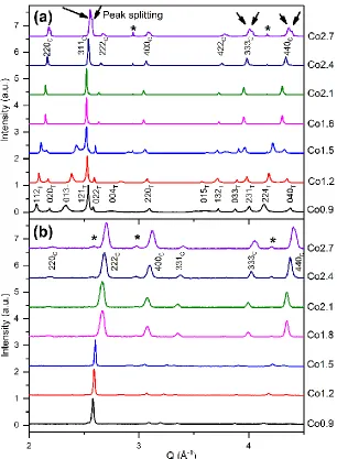
calcination temperature of 1400°C.The intensity is plotted in log scale for highlighting the secondary phase cristobalite SiO2 ... 70 Figure 5-1 (a) High resolution XRD and (b) ND patterns for all the CMO compositions at a selected 𝑄 range. The major reflections of the cubic and tetragonal spinel structures are noted. Asterisks indicate the presence of a secondary CoO phase. ... 78 Figure 5-2 Representative crystallographic structure refinement for Co0.9. The
HRXRD diffraction is shown in black, the calculated fit in red, and the difference in
blue. The hkl markers for tetragonal CMO phase used for refinement are in pink. ... 79 Figure 5-3 Representative crystallographic structure refinement for Co2.1 using
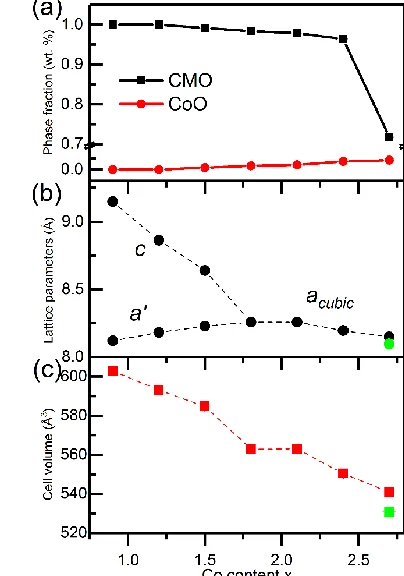
combined analysis of (a) ND and (b) XRD data. The diffraction is shown in black, the calculated fit in red, and the difference in blue. The hkl markers for cubic CMO phase used for refinement are in pink, and green for CoO phase. ... 80 Figure 5-4 (a) Phase fraction, (b) lattice parameters of CMO phase, and (c) unit cell
volume of CMO phase as a function of Co content. Error bars are shown and most
error bars are less than the symbol size. ... 81 Figure 5-5 (a) Metal-Metal and (b) Metal-Oxygen bond lengths as a function of Co
content in CMO ceramics. ... 83 Figure 5-6 𝑈iso of Co on A-sites, Co on B-sites, Mn on B-sites, and oxygen atoms for
cubic spinel CMO as a function of Co content. ... 84 Figure 6-1 Temperature dependent dielectric permittivity (ε’) and dielectric loss (tan δ) at various frequencies for BT-xBZT, where x=0.06, 0.08, 0.10, and 0.20 respectively
(arrows indicate the direction of increasing frequency). ... 93 Figure 6-2 (a) Reduced structure function, 𝑄(𝑆(𝑄) − 1), of BT-0.06BZT at room
temperature. The inset is a magnification of the high-Q region, indicating excellent signal-to-noise ratio. (b) PDF of BT-0.06BZT at room temperature after Fourier transform, the inset shows magnified area of low-r PDF data, and the major atom pairs which contribute to the local PDF peaks are indicated. ... 96 Figure 6-3 The fits of BT-0.06BZT room temperature PDF pattern over a range of 2-10 Å and 10-30 Å using four plausible phases: 𝑃4𝑚𝑚, 𝑅3𝑚, 𝐴𝑚𝑚2, and 𝑃𝑚3𝑚. The
goodness of fit value for each fit is listed. ... 98 Figure 6-4 The box-car fitting results of the lattice parameters a and c for BT-xBZT
using 𝑃4𝑚𝑚 model. The black and red shade lines in each subplot represent the a and c values with standard deviation obtained from whole profile fitting of PDF data
Figure 6-5 The PDF patterns of BT-0.06BZT at selected temperatures obtained by the
in situ high temperature total scattering technique. ... 103 Figure 6-6 Structure information of BT-0.06BZT as a function of temperature extracted from sequential whole profile fitting of temperature series PDF patterns: (a) lattice parameters a and c; (b) tetragonality(𝑐/𝑎); (c) unit cell volume; (d) anisotropic ADP of A-sites atoms where U11=U22≠U33 for 𝑃4𝑚𝑚. (e) and (f) show lattice parameters and
tetragonality in a magnified temperature range from 50°C to 150°C. ... 105 Figure 6-7 The lattice parameters of BT-xBZT average structures as a function of
temperature, where x=0.06, 0.08, 0.10, and 0.20. ... 108 Figure 6-8 The lattice parameters of BT-xBZT local structures as a function of
temperature, where x=0.06, 0.08, 0.10, and 0.20. ... 109 Figure 7-1 SEM image (a), dielectric measurements(b), and polarization loops (c) of
PMN-0.30PT ceramics. Inset of subplot (b) shows the deviation of Curie-Weiss law;
the dashed line shows the linear fit of (1/ε’) versus T at the paraelectric phase. ... 119 Figure 7-2 High-energy XRD pattern (a), reduced total scattering function (b), and PDF pattern after Fourier transform (c) of unpoled PMN-0.30PT ceramics. Asterisks in the
inset of (a) reveal traces amount of secondary pyrochlore phase. ... 122 Figure 7-3 (a): Magnified views of representative Bragg peaks of the high-energy XRD pattern, and the fits using different single phase models. The indices of these reflections are labeled in a pseudocubic unit cell. (b): the overall fit of the full pattern using
monoclinic Cm structure. ... 124 Figure 7-4 Fits of the unpoled PMN-0.30PT PDF pattern using different single phase
models over a range of 2-6 Å (representing the local scale structure), and over 8-28 Å
(representing intermediate scale structure). ... 126 Figure 7-5 (a): In situ electric field XRD in selected representative Q ranges. The
process is categorized into 3 stages. (b): the best fits using specific model for patterns at 1.5 kV/mm, 1.6 kV/mm, 2.2 kV/mm, and 4 kV/mm, respectively. Note for 4.0 kV/mm pattern a 𝑃4𝑚𝑚(red)+𝑃𝑚(black) mixed phase model was adopted. ... 128 Figure 7-6 Lattice parameters: cell edge length (a), β angle (b), and cell volume (c) of
polycrystalline PMN-0.30PT under various fields obtained from the Le Bail fitting. The assigned stage numbers and identified structures are noted. (d) schematic of polarization vector for R, MA, and T in a pseudocubic cell. (e) schematic of polarization vector for O, MB and MC. (f) Polarization rotation path for PMN-0.30PT ceramics
Figure 7-7 In situ electric field PDF patterns from 0 kV/mm to 4 kV/mm at different length scales. The arrows indicate the evolution of PDF peaks with increasing fields. The dashed lines in subplot (a) show the negligible changes of nearest and second
nearest Pb-Pb pairs with increasing field. ... 137 Figure 7-8 Representative fits of local PDF peaks from 3 Å to 4.5 Å under selected
fields. For the peak at r≈3.5 Å, subplot (a)-(d) shows 3-peaks model fits well for 0-1.8 kV/mm patterns. Subplot (e) and (f) compare the fit using 3-peaks model and 2-peaks model. Subplot (g) and (h) show 2-peaks model better represents the high-field local
CHAPTER 1 Introduction and Background 1.1 Introduction
Developing processing-structure-property relationships is the core of materials science and engineering. The ultimate goal for this interdisciplinary field is to obtain materials with desirable performance for various applications. A material’s performance is a combination of its properties, and a property is defined as the type and magnitude of the response to a specific imposed stimulus. The property of a material is a function of its structures at different length scales, ranging from macroscopic to subatomic level. The structure of a material strongly depends on the processing methods.[1] Therefore, the understanding of processing-structure-property relationships is crucial for guiding the design of materials with desirable properties and performance.
This study majorly focuses on the dielectric and ferroelectric properties in a variety of complex ceramics. Dielectric and ferroelectric materials are widely used in many applications, including capacitors, actuators, and transducers.[2], [3] Several fundamentally important dielectric and ferroelectric materials were investigated in this study, including:
these important dielectric and ferroelectric materials, primarily through the use of advanced X-ray and neutron diffraction and scattering techniques. The major techniques used in this study are: high energy X-ray diffraction (XRD), high resolution X-ray diffraction (HRXRD), neutron diffraction (ND), and X-ray total scattering. The combination of characterization techniques allow us to observe very interesting phenomena in complex dielectrics and ferroelectrics, such as the phase evolution during synthesis process, the phase changes under different processing conditions, and the responses of local and average structures under applied electric field. The crystallographic information obtained from these advanced diffraction and scattering techniques can be used to support the observed physical properties, and to construct the processing-structure-property relationships.
In this chapter, fundamental knowledge about the properties, structures, and processing of complex ceramics will be introduced.
1.2 Properties of Complex Functional Ceramics
and ferroelectrics. In this section, the dielectric, piezoelectric, and ferroelectric properties of these functional ceramics will be introduced.
1.2.1 Dielectrics and Dielectricity
Dielectric materials are electrically insulating and can exhibit polarization under the application of electric field. Polarization is the alignment of permanent or induced dipole moments with an externally applied electric field. There are four types of polarizations arising due to different mechanisms: electronic, ionic, dipole, and space charge, and each one corresponds to a specific frequency range.[5], [6] Figure 1-1 summarizes the different types of polarizations occurring in dielectrics. Some fundamental and important equations related to
the dielectricity are shown as follows.[1], [3] The electric displacement (𝐷𝑖) in a dielectric
material is related to the applied electric field 𝐸𝑗 through the relation:
𝐷𝑖 = 𝜖𝑖𝑗𝐸𝑗 ( 1-1 )
where 𝜖𝑖𝑗 is the dielectric permittivity of the material. The relative dielectric permittivity 𝜖𝑟,𝑖𝑗
can be calculated according to:
𝜖𝑟,𝑖𝑗 = 𝜖𝑖𝑗/𝜖0 ( 1-2 )
where 𝜖0 is the permittivity of free space. 𝜖𝑟 is usually used as a short notation of 𝜖𝑟,𝑖𝑗. The
dielectric permittivity is a complex number with real (𝜖𝑟′) and imaginary (𝜖
𝑟′′) components,
following the equation:
where tan(𝛿) refers to dielectric loss. The capacitance of the dielectric element can be determined by:
𝐶 = 𝜖𝑟𝜖0𝐴/𝑡 ( 1-4 )
where 𝐴 and 𝑡 are the area and thickness of the samples. Determination of the dielectric permittivity is generally important for the evaluation of device performance. Dielectric materials can be solids, liquids, or gases, but solids are the most commonly used dielectrics in the electrical engineering and industries.
1.2.2 Piezoelectrics and Piezoelectricity
Piezoelectricity refers to the linear coupling between mechanical stress and electric polarization and/or the linear coupling between mechanical strain and applied electric field in dielectrics. Piezoelectricity has two types of effects: direct effect where polarization occurs when a dimensional change is imposed, and converse effect where dimension change occurs when an electric field is applied.[7] Dielectric materials that display such reversible behaviors are called piezoelectrics. The piezoelectricity is described by an interrelation of four different electrical and mechanical variables: electric field 𝐸, strain 𝑆, mechanical stress 𝑇, and electric displacement 𝐷. Piezoelectric stress coefficients 𝑑 is defined as the mechanical response at
constant electric field or as the electric response at constant mechanical stress, formulated as:
𝑑 = (∂𝑆 ∂𝐸)𝑇 = (
∂𝐷
∂𝑇)𝐸 ( 1-5 )
The piezoelectric coefficient is actually a third rank tensor, since strain or electric displacement is a second rank tensor while electric field or stress is first rank tensor.[8]–[10]
Piezoelectricity is a reversible property exhibited in a select group of dielectric materials that don’t have a center of symmetry. Of the 32 crystal classes, 21 are
1.2.3 Ferroelectrics and Ferroelectricity
A ferroelectric material is a piezoelectric that exhibits a spontaneous polarization in the absence of an externally field, and the polarization can be reoriented by an applied field.[11], [12] The spontaneous polarization in a ferroelectric material results from the offset of the positive and negative charge centers in a unit cell, forming permanent dipoles. A ferroelectric ceramic consists of multiple grains, and each grain is composed of regions called domains. In each domain, the interactions between adjacent permanent dipoles lead to the mutual alignment in the same direction. Therefore, the polarization directions are the same inside each domain, but different between adjacent domains. In general, the size of ferroelectric domains ranges from a few nanometers to tens of micrometers.[13], [14] The interface between two domains is called the domain wall, with a thickness of a few unit cells. The existence of domain walls can reduce the elastic energy generated by the strain, minimizing the total free energy.[13], [15] Due to the random distribution of grains and domains, the as-processed ferroelectric ceramics don’t exhibit an overall polarization. The direction of the spontaneous polarization
can be reoriented with a sufficiently strong electric field, and this process is called poling. After poling, a net macroscopic polarization can be introduced in ferroelectric ceramics.
Two methods are normally used to characterize the macroscopic ferroelectricity of a specific material: polarization-electric field (P-E) and strain-electric field (S-E) measurements. In a P-E measurement, the macroscopic polarization is obtained by measuring the dielectric displacement on the dielectrics during the application of electric fields. An example of P-E hysteresis loop is shown in Fig. 1-2a. In an S-E measurement, the macroscopic strain is recorded during the application of electric field. An example of P-E hysteresis loop is shown Fig. 1-2b. A more thorough explanation to the P-E and S-E loops can be found in Ref. [14]
As mentioned in the above section, there are 20 piezoelectric crystal classes, and 10 of them pose a unique polar axis, showing the existence of a spontaneous polarization. These materials are called pyroelectrics, and if such spontaneous polarization can be reversed by external field, it belongs to ferroelectrics.[3] Most ferroelectric materials exhibit a structural phase transition or a series of phase transitions upon heating or cooling. Starting from a
temperature non-ferroelectric phase, which is called a paraelectric phase, into a low-temperature ferroelectric phase. Some ferroelectrics also exhibit several phase transitions while the temperature further decreases. An example of the phase transitions of a classic ferroelectric material, BaTiO3 (BT), is demonstrated in Fig. 1-3.
1.2.4 Relaxor Ferroelectrics
Relaxor ferroelectrics are a class of ferroelectric materials that show a broad maximum in temperature dependence of the dielectric permittivity, whose position, 𝑇m, is shifted to lower
temperatures as the frequency of the probing field decreases.[16], [17] The other features to distinguish a relaxor ferroelectric from a normal ferroelectric are: the absence of macroscopic ferroelectric transition, lack of macroscopic spontaneous polarization, and a ferroelectric-like response after cooling to a low temperature under application of field.[16], [18]–[21] Relaxor ferroelectrics exhibit an enormous electromechanical response and are easily polarized with an external field. These properties make them attractive for applications such as sensors and actuators. Local clusters of randomly oriented polarization, known as polar nanoregions (PNRs), are specific to relaxor ferroelectrics and play a key role in governing their interesting properties.[16], [17], [21]–[24] Figure 1-4 shows the comparison between a normal ferroelectric and a relaxor material.[25] The relaxor behavior was first observed in the perovskites with disorder of non-isovalent ions, including the stoichiometric complex perovskite compounds, e.g. Pb(Mg1/3Nb2/3)O3 (PMN) and nonstoichiometric solid solutions, e.g. La-doped Pb(Zr1-x, Tix)O3 (PZT).[26]–[29] Since then, relaxor behaviors have been
reported in various types of materials, e.g. perovskite structures, tetragonal tungsten bronze structures, and aurivillius structures.[17] The existence of polar nanoregions in relaxor ferroelectrics is evidenced by measurements of the temperature dependence of the optic index of refraction, neutron diffuse scattering, and transmission electron microscopy.[30]–[34] The size of polar nanoregions is very small, of the order of a few nanometers. Even though the crystal structure of PNRs is thought to be different from the non-polar regions, structural characterization only shows a cubic symmetry on average.[16], [17] Other local probes are needed to describe the structures in PNRs. Basically, there are two models to illustrate the PNRs in relaxor ferroelectrics, as illustrated in Fig. 1-5. For the first model, the PNRs are embedded in the non-polar matrix with a cubic symmetry. For the second model, the PNRs with low-symmetry are separated by domain walls, in which the thickness of domain walls is comparable with the size of PNRs. Although relaxor ferroelectrics have been widely used in various applications, the cause and mechanisms of the PNRs formation are not conclusively understood, and the structure-property relationship demands deeper investigation.
1.3 Crystal structures
The crystal structure of a material describes the manner in which atoms, ions, or molecules are spatially arranged. In order to predict and to rationalize the crystal structures of ionic compounds, Pauling proposed a series of principles, which are called Pauling’s rules. According to the Pauling’s rules, a crystal structure of a typical solid ionic compound is
parsimony.[35] The combinations and interactions between different atoms result to the diversity of crystal structures in ceramics. Three major types of crystal structures are:
1). AX-Type, where A is cation and X is anion. This is the simplest structure in ceramics, for which the number of cations and anions are equal. Some common structures in ceramics are rock salt, cesium chloride, and zinc blende.
2). AmXp-Type, in which the charges on the cations and anions are not the same. An example is AX2, a typical crystal structure for which is fluorite.
3). AmBnXp-Type, for which more than one type of cations (A and B here) contain in the materials. The most representative structures in this type are perovskite and spinel.
1.3.1 Perovskites
A lot of the widely used dielectric and ferroelectric materials have a perovskite structure.[4] Perovskite materials have a chemical formula of ABO3, where A and B are different types of cations located at different sites of the unit cell. The general perovskite structure can be thought as a primitive cubic, with A-site atoms located at the corners, B-site atoms at the body center, and oxygen atoms at centers of six faces. For a prototypic perovskite with cubic symmetry, the coordination number of the A-site atoms is 12 and the B-site atoms is 6. A representative perovskite structure is shown in Fig. 1-6a and b. Perovskite structure is flexible, and can tolerate different types of cations on A- and B-sites as long as the charge neutrality is maintained.
perovskite structure is PZT, in which the A-sites are occupied by Pb2+ while B-sites are co-occupied by Zr4+ and Ti4+. The best known canonical relaxor ferroelectrics, PMN, also has a perovskite structure. For PMN, the B-site is co-occupied by Mg2+ and Nb5+, and in order to maintain the charge neutrality, the atomic concentration fraction is Mg:Nb = 1:2. Due to the lead toxicity, a lot of efforts have been made to develop lead-free ferroelectrics that have comparable properties with the lead-based materials. There are three types of lead-free ferroelectric systems that are widely investigated: BaTiO3-based, (Na, K)NbO3-based, and (Na, Bi)TiO3-based.[14], [36], [37]
The properties of these lead-based and lead-free ferroelectrics can be tuned by chemical modification. It is worthwhile to note that the fundamental origins of the physical properties in both lead-based and lead-free systems remain unknown, and studying these systems can have scientific and technical impacts on the ferroelectrics community. In this dissertation, two lead-free systems, NBT-xBT and BT-xBZT, and one lead-based systems, PMN-xPT, are investigated as examples to study the processing-structure-property relationships in complex dielectric and ferroelectric materials with perovskite structures. These three materials are briefly introduced as follows.
Na1/2Bi1/2TiO3-xBaTiO3 :
Na1/2Bi1/2TiO3 (NBT) has a high Curie temperature (𝑇C) of 325°C and a piezoelectric constant (𝑑33) of 73 pC/N, making it a promising candidate for lead-free ferroelectrics.[38],
[39] The piezoelectric and ferroelectric properties can be enhanced by forming a solid solution of NBT with the classic ferroelectric material BT, often referred as NBT-xBT.[40], [41] In this material, the B-sites are occupied by Ti4+ exclusively, while A-sites have three different cations: Bi3+, Na+, and Ba2+. A phase diagram is shown in Fig. 1-7, in which a morphotropic phase boundary (MPB) is found at 6-7 mol% BT between the NBT-rich rhombohedral and BT-rich tetragonal phases.
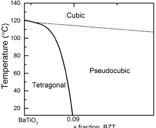
BaTiO3-xBi(Zn1/2Ti1/2)O3:
When modifying the classic ferroelectric BT with Bi(Zn1/2Ti1/2)O3 (BZT), a solid solution of BT-xBZT is obtained. In BT-xBZT, the A-sites are co-occupied by Ba2+ and Bi3+, while B-sites are co-occupied by Zn2+ and Ti4+. BT-BZT was firstly reported by Huang et al.[42] Since then, many property characterization and structure determination studies were
conducted on this material. Previous dielectric measurements show a crossover from normal ferroelectric-like behavior to relaxor-like behavior when the BZT concentration increases to x
= 9%.[42]–[44] Laboratory XRD suggests a phase transition from tetragonal to ‘rhombohedral-like’ (or pseudocubic) structure with increasing BZT concentration in this solid solution, and
a critical composition for this transition is around x = 0.09.[42], [45] The phase diagram of
BT-xBZT is shown in Fig. 1-8. BT-xBZT has high temperature stable performance, making it a good candidate for high temperature capacitors.[46]
Pb(Mg1/3Nb2/3)O3-xPbTiO3:
The PMN-xPT solid solution is formed by incorporating a classic lead-based ferroelectric PbTiO3 (PT) into a traditional relaxor-ferroelectric PMN. In this material system,
Pb2+ cations are on the A-sites exclusively, while B-sites are co-occupied by Mg2+, Nb5+ and Ti4+. With the addition of PT, the Curie point and the non-hysteretic quadratic strains increased. Also, it was found that with increased PT concentration, the relaxor behavior was gradually replaced by a typical ferroelectric behavior.[47]–[49] The transition from relaxor to ferroelectric forms a PMN-xPT binary phase diagram, and a MPB was obtained around x = 0.30-0.35, separating the rhombohedral and tetragonal structures.[47] The current phase diagram for PMN-xPT can be found in Fig. 1-9. An enhanced piezoelectric response of
PMN-xPT was observed when approaching the MPB. A number of mechanisms have been proposed
to explain the high piezoelectric activity by considering the diversity and instability of ferroelectric phases at MPB, such as ‘electric field-induced phase transition’, ‘ease of polarization rotation via a monoclinic phase’, ‘adaptive domain structure’, and ‘existence of polar nanoregions’.[50]–[55]
1.3.2 Fluorites
In addition to the dielectrics with a perovskite structure, fluorite-based dielectrics also
play important roles in the semiconductor industries. The structure name, fluorite, comes
to the desirable dielectric properties, HfO2 is used as a high-𝑘 material in semiconductor
industries.[56], [57]
The ferroelectricity and antiferroelectricity in thin HfO2-based thin films were first discovered in 2007 by Böscke et al.[58] Followed studies show that the ferroelectric behavior
can be obtained when HfO2 is processed with a specific combination of chemical doping and processing conditions. The previous works show that a certain compositional range of doping (e.g. Si, Al, Y, Zr, Sr, La, and Gd), as well as a unique stress state, are required to induce ferroelectricity in HfO2 thin films.[57], [59]–[61] HfO2 has various polymorphs in bulk phases depending on the temperature and pressure. A transition from monoclinic to tetragonal to cubic phase occurs during heating from room temperature to 2773K. However, the inversion symmetry of these space groups prohibits ferroelectricity and related functionalities. The structural origin of the observed ferroelectricity is thought to be the existence of a polar 𝑃𝑐𝑎2
structure under different stress, chemical or surface conditions, and this has been discussed experimentally and theoretically.[62]
1.3.3 Spinels
temperature coefficient (NTC) thermistor application given that the strong electron correlations in Mn can induce semiconducting characteristics with moderate resistivity at room temperature.[64], [65] Within this CoMn2O4 spinel structure, the O2- anions form a FCC lattice, whereas Co2+ cations fill tetrahedral sites and Mn3+ cations occupies the octahedral positions. The structure is presented in Fig. 1-6d.
1.4 Ceramics Processing
Traditionally, most of the ceramic materials are prepared by solid state synthesis method in which high temperature is required to accelerate the slow solid-solid diffusion.[1], [4] Processing methods can significantly affect the final products’ microstructure, phase, and crystal structure. Therefore, it is important to optimize the ceramic processing conditions in order to obtain desirable properties. Some basic and important processing steps for solid state ceramic preparation are induced as follows.
Batching and Milling:
In addition, it usually adds impurities to the powder from the milling media. The other milling method used is vibratory milling, the drum containing the media and powder is vigorously shaken. The collisions between the media are much more violent than in ball milling, therefore the milling time is shorter and powders are finer.
Calcination:
After milling, drying, and sieving, the dried powders were calcined at elevated temperatures for a given time depending on the processing details for the specific material systems. Calcination reactions usually take place at or above the thermal decomposition temperature (for decomposition and volatilization reactions) or above the transition temperature (for phase transitions). The goal of calcination in ceramic processing is to induce phase transformation and solid-solid reaction. The calcination process was performed in an air atmosphere with a heating and cooling rate controlled by programmable furnace. The dried powders were contained in a closed alumina crucible for the calcinations. After calcination, the calcined powders were milled to eliminate particle agglomerations.
Sintering:
reduction in total particle surface area. Sintering is carried out below the melting temperature, so that a liquid phase is normally not present.
1.5 Dissertation Overview
In this dissertation, the processing-structure-property relationships for multiple complex dielectrics and ferroelectrics are studied using advanced scattering techniques. The dissertation is organized as follows. Chapter 2 introduces the structure characterization and data analysis methods which are used throughout the entire study. In Chapter 3, the processing-structure relationship of NBT-xBT is investigated using in situ XRD technique during the solid state synthesis. The phase evolution behaviors and reaction sequences are observed, and a new formation mechanism for NBT-xBT during solid state synthesis is proposed based on the interpretation of the in situ XRD results. In Chapter 4, the crystallographic structures for Si-doped HfO2 is studied using HRXRD and Rietveld refinement method. The processing conditions for obtaining non-equilibrium Si-doped HfO2 is determined in this study. Chapter 5 gives a comprehensive structure characterization of CMO spinel compounds using combined analysis of neutron and X-ray diffraction in order to understand the relationship between the CMO structures and their electric properties. Chapter 6 studies the structural evolution of
CHAPTER 2 Advanced Scattering Techniques and Data Analysis Methods 2.1 Background
Diffraction and scattering and techniques are widely used in structural determination of materials at atomic and subatomic levels. Due to historic reasons, some terms (even the “scattering” and “diffraction” themselves) are often used differently (and sometimes
imprecisely) in different communities, leading to confusion and misunderstanding. To be precise and consistence, some important terms related to this dissertation are clarified as follows.
Based on if one scattering event is elastic or inelastic, and if it is coherent or incoherent, all the scattering processes can be categorized into four groups: elastic and coherent, inelastic and coherent, elastic and incoherent, and inelastic and incoherent process. Since structural information in the scattering comes from the interference effects, only coherent scattering contains structural information of interest in this dissertation. Among different scattering events, Bragg diffraction is elastic and coherent, thermal diffuse scattering is inelastic and coherent, and Compton scattering is inelastic and incoherent.[69]
2.2 Structural Characterization with Diffraction Techniques
According to the above definitions, a Bragg diffraction phenomenon is a subset of scattering, and is often called as diffraction for simplicity. The diffraction is primarily concerned by the crystallographic and material scientists due to the constructive and destructive interferences, which can be used to interpret the periodic arrangement of atoms in the materials. The beam used to interact with matters in the scattering and diffraction techniques can be X-rays, neutrons, and electrons. In this chapter, several types of diffraction techniques using X-rays and neutrons will be introduced.
2.2.1 Laboratory X-ray Diffraction
Cu and Mo. Other elements, e.g. Cr, Co, Ag, etc., can be used for specific applications.[67], [68] There are two principal types of geometries for laboratory X-ray diffractometers: reflection and transmission. In reflection geometry, the sample is in the form of a flat plate, while in transmission geometry a glass capillary or thin foil is used. The schematics of these
two geometries are shown in Fig. 2-1a and b.
2.2.2 Synchrotron X-Ray Diffraction
X-rays can also be generated from synchrotron sources. The use of synchrotron X-ray radiation has several advantages over laboratory sources, such as high flux, high resolution, and high energy. Synchrotron radiation is extremely intense, and highly collimated. The synchrotron X-ray sources used in this work for diffraction studies are beamline 11-BM-B with the bending magnets (BM), and beamline 11-ID-C with the insertion devices (ID) (e.g. wigglers and undulators) at Advanced Photon Source at Argonne National Laboratory.
Beamline 11-BM-B is equipped with high resolution detectors. The obtained patterns can show more subtle features that is absent in laboratory diffractometers. Using the high
resolution data can yield a more accurate description of the crystal structure. Beamline 11-ID-C is equipped with a 2D area detector, and works in transmission mode. The high flux and high energy features of this beamline offer faster data acquisition speeds, larger penetration depth, and wider coverage of the scattering angle. The 2D area detector allows texture analysis and anisotropic structural changes under different stimuli (e.g. electric field, stress, and pressure). In this study, synchrotron XRD was performed on Si-doped HfO2 to investigate the processing-structure relationships as described in Chapter 4.
2.2.3 Neutron Diffraction
Neutron diffraction is a similar technique compared to XRD, but due to some unique scattering properties, it has several advantages. Since neutrons scatter through nuclear interactions, neutron diffraction has a low absorption coefficient and high penetration for most of the elements. The neutron scattering strength is not dependent on the atomic number. It is possible to observe the effect of light elements in the presence of heavy ones in the neutron diffraction patterns. In addition, neutrons have a magnetic moment and their scattering is sensitive to the magnetic moment of atoms, making neutron scattering the ideal approach to study magnetic materials.[68]
United States. For a spallation source, the neutron is generated by bombarding energetic particles (e.g. protons) into a heavy-metal target (e.g. Pb or Hg). The spallation facility used in this study is beamline BL-11A Powder Diffractometer (POWGEN) at the Spallation Neutron Source at Oak Ridge National Laboratory.
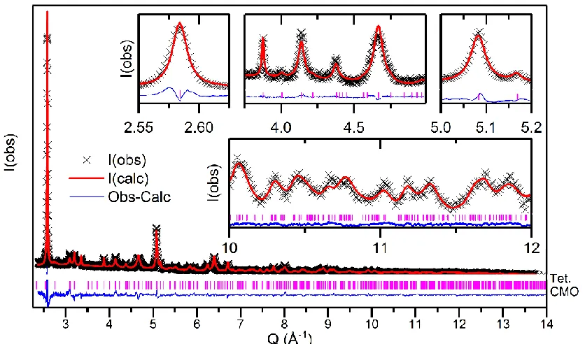
Note that neutrons and X-rays provide complementary structural information of the material, therefore, more precise structural parameters can be obtained by a combined analysis of X-ray and neutron diffraction data. Combined analysis of neutron and X-ray diffraction was performed on CMO spinel oxides to investigate the structure-property relationship, as described in Chapter 5.
2.2.4 In situ Diffraction Techniques
In situ diffraction is a powerful technique to study the processing-structure-property relationships, and has been widely applied to study dielectrics and ferroelectrics.[70], [71] In situ diffraction measurements can be performed during the material processing. The collected patterns as a function of reaction time/temperature can be used to study the formation mechanisms, such as nucleation, crystallization, phase growth, phase evolution, and diffusion, etc.[70], [71] Therefore, it gives better understanding of the processing-structure relationship in the materials. In this study, in situ diffraction during synthesis was conducted and described in Chapter 3.
provide useful information about the field-responsive mechanisms of ferroelectric materials, such as field-induced lattice strain, domain wall motion, and field-induced phase transition.[70], [71] In this work, in situ diffraction under electric field is described and studied in Chapter 7. A representative schematic for in situ synchrotron diffraction measurement of ferroelectrics under application of electric field can be seen in Fig. 2-2.
2.2.5 Analysis of Diffraction Data
phase identification, single peak fitting, Rietveld refinement, Le Bail fitting, are briefly introduced as follows.
Phases contained in a diffraction pattern can be identified by crystallographic database matching. The characteristic diffraction pattern generated in a typical diffraction measurement provides a unique “fingerprint” of the crystals present in the sample. Therefore, by comparing
the measured diffraction pattern with standard references in the XRD database, the crystallographic structures and phases can be identified.[66], [68] The crystallographic databases contained structural information of innumerous phases and materials, and the most widely used database nowadays is the International Centre for Diffraction Data (ICDD) database.
Single peak fitting can be used to extract the peak position, full width at half maximum (FWHM), and peak intensity. Peak fitting is extremely useful to study the structural changes under applied stimuli. Each measured diffraction peak can be modeled by proper profile shape functions, such as Gaussian, Lorentzian, Pearson VII, or Pseudo-Voigt.[70], [72] The choice of shape functions depends upon the instruments used for the measurements. By peak fitting, the lattice parameters, lattice strain, crystallite size, and domain reorientation can be calculated.
refinement has been incorporated into most of the structure analysis software such as General Structure Analysis System (GSAS)[75], FullProf Suite[76], Materials Analysis Using Diffraction (MAUD)[77], and GSAS-II[78].
suitable for attempting a structure solution. Both methods were derived from the Rietveld refinement method. The use of Le Bail fitting method to determine the structural changes under application of field can be found in Chapter 7.
2.3 Structural Characterization with Total Scattering Techniques
Noticeably, more and more advanced materials with high performance or precise response are demanded in order to satisfy the rapid development of nowadays technology. Normally these advanced materials have a sophisticated or complex crystal structure due to the competing and balancing of the internal forces at local scale, even though on average the structure is quite simple and straightforward.[69], [81] To study and design such complex materials, it is important to better understand the structures in atomic and nanometer scale.
An alternate approach for local scale structure studies, called total scattering, was utilized in this work. In general, the total intensity collected from a scattering event between a beam and a matter, 𝐼𝑇, contains several parts:
𝐼𝑇 = 𝐼𝐶+ 𝐼𝐼𝐶+ 𝐼𝑀𝐶+ 𝐼𝐵𝐺 ( 2-1 )
where 𝐼𝐶 is the coherent scattering intensity, 𝐼𝐼𝐶 is the incoherent scattering intensity, 𝐼𝑀𝐶 is the multiple-scattering intensity, and 𝐼𝐵𝐺 the background intensity. As mentioned before, only
the coherent scattering part (𝐼𝐶) contains information for structure interpretation of the matter.
And the coherent scattering intensity 𝐼𝐶 is composed of elastic coherent scattering (Bragg
diffraction and elastic diffuse scattering) and inelastic coherent scattering (e.g. inelastic diffuse scattering). The total scattering technique measures the coherent scattering in a wide range of 2θ (or momentum transfer 𝑄), and treats the Bragg diffraction and diffuse scattering
contributions equally.[69], [81] The local scale structural information that is contained in the total scattering pattern can be analyzed either directly in the reciprocal space, or in real space using pair distribution function (PDF), as described below.
2.3.1 Pair Distribution Function
PDF is obtained by applying a Fourier transform to a total scattering pattern, as:
𝐺(𝑟) = 2
𝜋∫ 𝑄[𝑆(𝑄) − 1] sin(𝑄𝑟) 𝑑𝑄 ( 2-2 )
the atom-atom distance. The inverse transformation yields the structure function 𝑆(𝑄) in terms of 𝐺(𝑟), as:
𝑆(𝑄) = 1 + 1
𝑄∫ 𝐺(𝑟) sin(𝑄𝑟) 𝑑𝑟 ( 2-3 )
Thanks to the development of spallation neutron sources, X-ray synchrotron sources, as well as the high-speed computing, the PDF method has become increasingly accurate and reliable to study the local structure of various materials such as amorphous, nanomaterials, and complex ceramics.
or higher, depending on the Q resolution).[83] Thus not only the short-range but also the medium-range structure can be readily obtained in PDF. Compared to EXAFS, the PDF technique is not limited by the elements in the system nor their absorption edges, and is more broadly applicable. The atomic correlation of specific elements, and the contributions to the PDF from different atom pairs can be derived from models after refinement of PDF data. Considering the different features offered by EXAFS and PDF, it is beneficial to utilize both datasets in Reverse Monte Carlo method, giving additional constrains to the models.[81], [84] Based on the radiation sources, the PDF measurements can be categorized into three types: X-ray, neutron, and electron PDF. In the following, X-ray and neutron PDF are briefly introduced. Modern approach to X-ray PDF measurements is the use of synchrotrons radiation facilities such as the Advanced Photon Source at Argonne National Laboratory. Synchrotron PDF has several advantages such as high energy, high flux beam, sensitive detectors, and fast readout. The synchrotron PDF experiments in this work were performed at beamline 11-ID-B at Advanced Photon Source. Neutron total scattering is also particularly powerful, especially in the study of dielectric and ferroelectric ceramics. Since the neutron scattering length is not proportional to the atomic number, the lighter atoms (e.g. oxygen in ceramics) are more visible under neutron scattering compared to the X-ray scattering techniques. The spallation neutron source can provide ample intensity of epithermal neutrons with higher energies, suitable for PDF measurements.[81], [84] The neutron PDF can be collected at beamline BL-1B at SNS using the Nanoscale-Ordered Materials Diffractometer (NOMAD).
scattering structure function 𝑆(𝑄) with high accuracy, which will be used for the inverse
Fourier transform to generate PDF. Some important data processing steps are briefly introduced as follows.
Firstly, the scattering signal from the addenda (e.g. sample container, background, sample environment, etc.) need to be removed. A series of total scattering measurements need to be performed, including scattering without the sample, without the sample and sample environment (e.g. insulating liquid), and scattering purely from the background. Thereafter, the contributions of scattering signal from each addendum can be determined and subtracted. Absorption corrections are necessary for samples that highly absorb X-rays. This step requires linear attenuation coefficients for the sample and container. If the sample composition and sample density are known, the attenuation coefficients can be calculated.[67], [69]
In addition to the scattering events that the photons only scattered once, in reality, some photons may be scattered multiple times before being collected by the detector. This multiple-scattering effect need to be corrected. Multiple multiple-scattering effect is most significant in transmission geometry at high scattering angles.[68], [69]
processing. The Compton scattered intensity can be calculated theoretically and subtracted.[69], [85], [86]
The properly corrected and normalized 𝑆(𝑄) is obtained only after these steps. Great
care is needed in order to avoid the misleading interpretations of the PDF data. Most of the corrections are well understood and can be reliably estimated by various softwares or programs, such as PDFgetX3 and PDFgetX2.[87], [88]
2.3.2 In situ PDF Techniques
Similar to the diffraction measurements, a PDF measurement can be conducted in situ
during the application of stimuli. Using this in situ technique, the local structural changes can be monitored and analyzed, giving better understanding of the structure-property relationship in complex materials. In this work, the in situ high temperature PDF was conducted on
BT-xBZT material systems, as described in Chapter 6; and in situ electric field PDF is conducted on PMN-xPT in Chapter 7. A representative schematic for in situ synchrotron total scattering measurements of ferroelectrics under application of electric field can be found in Fig. 2-3.
distinctly different orientations relative to the field vector. The scattering information that represents a fixed scattering vector angle to the field vector can be extracted using the 2-D area detector.[70], [71] Usually, two types of directional total scattering data, in which the scattering vector is parallel and perpendicular to electric field, are analyzed for the field induced structure anisotropy. After an inverse Fourier transform of the directional total scattering data, directional PDF patterns are obtained. the directional PDF describes the atom-atom pair distances along a given direction in polycrystalline ceramics. For example, for PDF pattern parallel to electric field direction as shown in Fig. 2-4, each peak is associated with atom-atom
pairs that are parallel to the external field. In other words, in an ABO3 perovskite structure, the peak at around 3.3 Å in PDF pattern parallel to electric field, is a reflection of the nearest A-B pairs parallel to field in crystallites with <111> parallel to field, and the peak at around 4 Å is a reflection of the nearest A-A or B-B pairs parallel to field in crystallites with <001> parallel to field, and so on.[89], [90] In summary, each PDF peak in the directional PDF comes from different crystallites with different orientations to the electric field.
2.3.3 PDF Data Analysis
A lot of information can be obtained by careful analysis of the PDF data. The PDF patterns can be studied directly without employing a structure model (peak fitting) or by structural modeling (real space PDF refinement).
In general, a PDF peak has a Gaussian-like shape because it results from a distribution of atom-atom distance by atomic disorder, and each peak is actually a sum of a series of delta functions over the entire scatted matter. By simply fitting the individual PDF peaks, valuable information can be revealed: the position gives the average separation of the pair of atoms; the integrated intensity yields the coordination number of that pair of atoms; and the width and shape of the peak gives the underlying atomic probability distribution.[69]
The positions of PDF peaks are direct reflections of the bond lengths and atom-atom pair distances within the material. The peak position can be accurately determined by fitting the individual peak with a Gaussian function. Usually for a disordered material, the nearest neighbor distance (first PDF peak) is well defined. While the atom-atom distances at longer distance are less well defined, and the peaks become broader, but still maintain their existence. But for a well-ordered crystal, the atom-atom pairs at all length scales are well defined due to the long-range order, resulting to sharp PDF peaks. Note that ideally the well-defined peaks can persist at infinite length for ordered crystals, but in practice the peaks at high r are limited by the instrument resolution. The pair distance information can give insights of the coordination geometries, helps to develop the accurate structure models.
correlation can be monitored by extracting the PDF peak area under different conditions. Note that for a system with only one element, the abundance of the correlation is the coordination number of that pair of atoms. But for a material with multiple elements, the weighting factors of each element need to be counted in order to obtain the coordination number information.[69], [81]
The width and shape of PDF peaks gives information about the atomic probability distribution. In general, the Gaussian-shaped PDF peaks result from distribution of atom-atom distances by the thermal or static displacements induced atomic disorder. If the probability distribution is non-Gaussian, the PDF will reflect this feature. In addition, the slope of the PDF at low r is related to the sample density.[69], [85]
Unlike EXAFS, the PDF technique is not an element-specific probe, but such structural and elemental information can be recovered by extending the PDF measurements to multiple related systems and using a differential analysis method. As mentioned in previous sections, the PDF pattern is a summation of all interatomic distances over the material. Therefore, the contributions of different components (different types of atom-atom pairs) are additive. For the differential analysis, if the PDF of one component can be accurately obtained, this PDF can serve as the reference, and other contributions of the total PDF can be subtracted and isolated. Note that the differential analysis is directly applied on the PDF patterns, instead of doing a Fourier transform of the difference pattern of the total scattering intensity pattern 𝐼(𝑄). This is
the 1 wt.% level and below. This method allows reliable analysis of multi-components systems, reveals valuable information that normal total PDF analysis cannot offer.[85]
Besides analyzing the PDF pattern by fitting individual peaks, more valuable information can be obtained from structural modeling. In this process, PDF data can be refined by minimizing the difference between the observed and the calculated PDF patterns using a regression algorithm. A variety of modeling approaches are available nowadays for the structure optimization. In general, these methods are classified into two categories, “Small Box” and “Big Box” modeling.
The “Small Box” approach means that a smallest possible unit cell is specified to reflect
the structure, and periodic boundary conditions are applied on the single unit cell for calculating the PDF of the material. Analogue to the Rietveld refinement method on powder diffraction data, the “Small Box” modeling is efficient to recover the crystallographic structure
at local scale. This real space Rietveld modeling method is integrated into PDFgui software.[91] A lot of structural information can be obtained from “Small Box” modeling, e.g. the lattice parameters, atomic positions, and atomic displacement parameters which reflect the static and dynamic disorder. In addition, other information, such as the average dimension of nanoparticles or length scale of structural coherence in disordered materials, can also be extracted. In the modeling process, the structure over various length scales can be determined by selecting different atom-atom distance (𝑟) range of the pattern. The “Small Box” method
neither. The real space PDF refinement can be conduct using different software packages, such as PDFgui[91] and DISCUS[92].
The “Big Box” method extends the model to multiple independent unit cells containing
a large number of atoms, and the size of the box is larger than the actual range of PDF data. This method utilizes reverse Monte Carlo algorithms, and is not subject to symmetry constraints. In the “Big Box” approach, the structural model is fit to the data by adjusting atom
CHAPTER 3 Formation Mechanism Study of NBT-xBT During Solid State Synthesis The content in this chapter was published with the title “Formation of Sodium Bismuth
Titanate-Barium Titanate during Solid State Synthesis”, in Journal of the American Ceramic Society. 2017;100:1330–1338.[93]
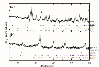
In this chapter, phase formation of NBT and its solid solutions NBT-xBT during the calcination process is studied using in situ high temperature diffraction. The reactant powders are mixed and heated to 1000°C, while XRD patterns are recorded continuously. Phase evolutions from starting materials to final perovskite products are observed, and different transient phases are identified. The formation mechanism of NBT and NBT-xBT perovskite structures is discussed, and a reaction sequence is suggested based on the observations. The in situ study leads to a new processing approach, which is the use of nano-TiO2, and gives insights to the particle size effect for solid state synthesis products. It is found that the use of nano-TiO2 as reactant powder accelerates the synthesis process, decreases the formation of transient phases, and helps to obtain phase-pure products using a lower thermal budget.
3.1 Introduction
system make it a viable alternative for certain applications in which PZT is currently utilized.[40], [41] In order to broaden the application range of NBT-xBT and make it as versatile as PZT, a better understanding of the underlying formation mechanism and various factors that affect the properties of NBT-xBT is necessary and critical.
In situ high temperature XRD is applied in the present work instead of ex situ
characterization methods. Nowadays, revolutionary improvements in laboratory powder diffraction systems enable studies of various material systems under applied stimulus (e.g. temperature, atmosphere, pressure, and electric field), which provides valuable structural information of structure-property relationships, changes in structures, and phase evolution with applied stimuli.[71], [95] Even though ex situ methods can offer less noisy XRD patterns due to higher sampling statistics and longer counting time, traditional quenching methods used in
ex situ methods limit the ability to capture phase evolution that happens in real time. To better understand the formation mechanism and phase evolution of NBT and NBT-xBT during solid state synthesis, in situ XRD patterns were obtained and investigated.
3.2 Experimental

![Figure 1-4 Comparison between normal ferroelectrics and relaxors.[25], [252]](https://thumb-us.123doks.com/thumbv2/123dok_us/1729469.1220818/25.612.129.465.347.696/figure-comparison-normal-ferroelectrics-relaxors.webp)