Abstract
HUSSAIN, YAZAN AHED. Stiction Reduction Agents Studies Using QCM. (Under the direction of Christine S. Grant.)
The problem of stiction in microelectromechanical systems (MEMS) is highly limiting their fabrication and functionality. The problem occurs during the fabrication,releasestiction, as well as during the use of the devices,in-use stiction. Anti-stiction agents are currently an active area of research in the MEMS field to address this issue. These agents are primarily deposited in the form of self-assembled monolayers (SAM’s) on the substrate to change its surface properties; to reduce what is known as the stiction problem. One commonly used SAM is the octadecyltrichlorosilane (OTS). On silicon substrates, the most used material in MEMS fabrication, OTS has shown high effectiveness in reducing devices stiction.
The use of a quartz crystal microbalance (QCM) as an analytical technique for studying the OTS anti-stiction agent is presented in this work. Using the QCM as the primary analytical tool, we were able to extract comprehensive information about the formed SAM. The dependence of SAM deposition on the bulk phase concentration of the deposit solution is shown. A rough estimation of the adsorption kinetics’ rate constants were calculated, and the equilibrium constant was determined from their values. The equilibrium constant shows the high favorability of OTS deposition on silicon substrate compared to the reverse desorption process. The complex nature of the OTS SAM and its formation mechanism were also shown. These conclusions were made based upon comparison between the more robust SAM system of thiols on gold and the OTS on silicon.
by
Yazan A. Hussain
a thesis submitted to the graduate faculty of north carolina state university
in partial fulfillment of the requirements for the degree of
master of science
department of chemical engineering
raleigh November 2003
approved by:
Dr. Christine Grant chair of advisory committee
Dr. Jacqueline Krim
Biography
Yazan A. Hussain was born in Zarqa, Jordan on the 20th of January, 1978. He is the fifth of four brothers and one sister. He studied the first five years of school in Saudia Arabia, after then he came back home, where he finished his school. In 1995, Yazan joined Jordan University of Science & Technology, where he obtained his B.S. with honors in Chemical Engineering in 2000.
In 2001, he came to the USA, where he joined the Chemical Engineering Department at NCSU as M.S. student. He joined Dr. Grant’s group, where he worked in the MEMS field.
First, I thank my parents, my brothers, and my sister for being my family. I love you!
I also thank my advisor, Dr. Christine Grant, for her support during this work, her understand-ing, and her patience. I also thank the former researchers, Manoj and Jeremy, who started this project, and my current group-mates, it is a pleasant group to be with.
I thank Dr. Krim and her students, Manju and B, for the discussions we had and for supplying the data for the lubricant uptake.
I also thank Chang, from Dr. Parsons’ group, for teaching me how to use the AFM. And Micheal, from Dr. Genzer’s group, for teaching me how to use the ellipsometer.
Finally, I acknowledge the NSF support for this work.
Table of Contents
List of Tables vii
List of Figures viii
1 INTRODUCTION 1
1.1 Historical Background . . . 2
1.2 Microfabrication . . . 3
1.2.1 Bulk Micromachining . . . 3
1.2.2 Surface Micromachining . . . 4
1.2.3 LIGA & Micromolding . . . 4
1.3 Materials in Microfabrication . . . 8
1.3.1 Single Crystal Silicon . . . 8
1.3.2 PolySilicon . . . 8
1.3.3 Silicon Dioxide . . . 9
1.3.4 Silicon Nitride . . . 9
1.3.5 Silicon Carbide . . . 9
1.3.6 Diamond . . . 10
1.3.7 Germanium . . . 10
1.3.8 III-V Materials . . . 10
1.3.9 Metals . . . 11
1.4 Limitations and Challenges in MEMS . . . 11
1.5 Project Overview . . . 13
2 PRELIMINARIES 15 2.1 Stiction Mechanisms . . . 15
2.1.1 Capillary force . . . 15
2.1.2 Solid bridging . . . 16
2.1.3 Van der Waal’s force . . . 17
2.1.4 Electrostatic forces . . . 17
2.1.5 Hydrogen bonding . . . 17
2.1.6 Asperity deformation force . . . 18
2.2 Adhesion Under Capillary Forces . . . 18
2.3 Current Stiction Solutions . . . 24
2.3.1 Process modification . . . 25
2.3.2 Surface modification techniques . . . 26
2.3.3 Surface energy reduction by organic monolayers . . . 28
2.4.2 Merits of SAM’s . . . 32
2.4.3 Common SAM systems . . . 33
2.4.4 Organosilicon SAM’s . . . 35
3 EXPERIMENTAL & MATERIALS 42 3.1 Quartz Crystal Microbalance . . . 43
3.1.1 Impedance analysis . . . 48
3.1.2 Factors affecting QCM behavior . . . 48
3.1.3 Applications of QCM . . . 51
3.1.4 Experimental setup . . . 52
3.2 Contact Angle . . . 54
3.3 Atomic Force Microscopy . . . 57
3.4 Experimental Procedure . . . 57
3.4.1 Cleaning . . . 57
3.4.2 QCM experiments . . . 59
3.4.3 Contact angle experiments . . . 60
3.4.4 Atomic force microscopy . . . 60
3.4.5 Materials . . . 61
4 RESULTS & DISCUSSION 62 4.1 Validation of Experimental Technique . . . 62
4.1.1 Selection of verification system . . . 62
4.1.2 Results & Discussion . . . 63
4.1.3 Conclusion . . . 67
4.2 Studies on the frequency effect on adsorption . . . 68
4.2.1 Theory . . . 69
4.2.2 Approach . . . 71
4.2.3 Results & discussion . . . 72
4.2.4 Conclusion . . . 73
4.3 Signal Stability & Analysis . . . 76
4.3.1 Noise reduction . . . 77
4.3.2 Temperature control . . . 79
4.3.3 ∆f determination . . . 80
4.4 Thiol Adsorption on Gold . . . 82
4.4.1 Why thiols? . . . 82
4.4.2 Compounds used . . . 84
4.4.3 Previous QCM studies on thiols . . . 84
4.4.4 Results & discussion . . . 84
4.5 Silane Adsorption on Si . . . 88
4.5.1 Literature survey on silane studies . . . 89
4.5.2 Results & discussion . . . 90
4.5.3 Kinetics studies . . . 98
4.5.4 Conclusion . . . 100
5 CONCLUSIONS & FUTURE WORK 102 5.1 Conclusions . . . 102 5.2 Future Work . . . 103
List of References 106
A Derivation of Electrical Components For QCM 116
B QCM runs summary table 121
1.1 Bulk vs. surface micromachining . . . 6
2.1 Comparison between different release techniques . . . 27
4.1 Kinematic viscosity measured by viscometer and QCM . . . 97
B.1 QCM runs for C12E8 on Au crystals . . . 122
List of Figures
1.1 Examples of positive and negative tone photoresists . . . 3
1.2 Schematic diagram of bulk micromachining . . . 5
1.3 Schematic diagram of the LIGA process . . . 7
1.4 Examples of fabricated MEMS devices . . . 13
2.1 Capillary forces caused by trapped liquid . . . 16
2.2 Solid bridging . . . 17
2.3 Equivalent contact model of two rough surfaces . . . 18
2.4 Comparison between stiction forces as a function of separation . . . 19
2.5 Contact angle relation with wettability . . . 20
2.6 Spring-plate-liquid system used to model adhesion in MEMS . . . 20
2.7 Constant volume curve showing the total energy change versus vertical spacing . . . 22
2.8 Branching diagrams for the spring-plate-liquid system . . . 23
2.9 Clamped beam adhering to its substrate . . . 24
2.10 Self-assembled-monolayer representation . . . 29
2.11 Convention used to represent 2D SAM structure . . . 30
2.12 Parameters used to represent the 3D SAM structure . . . 31
2.13 OTS adsorption mechanism . . . 39
3.1 Typical piezoelecric devices . . . 44
3.2 Assignment axes of qruartz crystal . . . 45
3.3 Butterworth-Van Dyke equivalent circuit for unperturbed quarts microbalance . . . 47
3.4 QCM crystal used in this work . . . 53
3.5 QCM crystal’s holder used in this work . . . 53
3.6 Setup used in QCM experiments . . . 54
3.7 Ram´e-Hart goniometer model 100-00 used for contact angle measurements . . . 56
4.1 Adsorption isotherm of C12E8 on gold . . . 64
4.2 Langmuir plot for C12E8on gold in aqueous solution at∼25◦C. . . 65
4.3 Adsorption isotherm for C12E8 on 5 MHz gold crystal to 9 MHz. . . 66
4.4 Scaled adsorption isotherm for C12E8 on 5 MHz gold crystals to 9 MHz crystals plus the oscillation effect . . . 67
4.5 Comparison between obtained and reference data . . . 68
4.6 Contact angles for Au slides coated with different concentrations of C12E8at ∼25◦C. 69 4.7 Shear waves generated by an oscillating surface . . . 70
4.8 Scaled experimental ∆f to account for oscillation effect . . . 71
4.9 The difference in ∆f between oscillating and non-oscillating crystals. . . 73
4.12 Comparison betweenin-situ andex-situ runs . . . 76
4.13 QCM response to surfactant addition and its relation with signal stability . . . 78
4.14 Stirring effect on QCM signal noise . . . 79
4.15 The change in solution temperature due to surfactant injection . . . 80
4.16 Temperature effect on QCM signal stability . . . 81
4.17 Some frequently used thiols for SAMs . . . 83
4.18 QCM signal response to different thiols . . . 85
4.19 QCM response to thiols with different chain lengths . . . 87
4.20 Langmuir isotherm fit to a thiol adsorption run . . . 88
4.21 Si QCM crystals response to OTS addition at different concentrations . . . 91
4.22 ∆f for 5 MHz Si crystals resulting from the addition of different OTS concentrations 91 4.23 The initial rate of change of f for 5 MHz Si crystals as a function of OTS concentration. 92 4.24 Chang in crystal frequency upon immersion in different solvents . . . 93
4.25 Relation between change in QCM frequency and solvent properites . . . 94
4.26 Comaprison between ∆f for OTS, thiols, and C12E8 . . . 95
4.27 Change in overall ∆V for the three systems used in this work. . . 97
4.28 Langmuir isotherm fit to OTS adsorption . . . 99
4.29 Determination of OTS adsorption rate constants . . . 100
5.1 ∆f for the uptake QCM measurements of vapor phase lubricant TBPP . . . 104
5.2 Change in amplitude for the uptake QCM measurements of vapor phase lubricant TBPP . . . 105
Chapter 1
INTRODUCTION
The problems that arise when a certain device is scaled, either up-to-down or bottom-up, are due to two facts. First, the change in dimensions will be combined with a respective change in surface area-to-volume ratio. For example, if a cubic box of 1 m length is scaled down to 0.5 m, the surface area-to-volume ratio will change from 6 m−1 to 12 m−1. Therefore, the corresponding external
forces that act on the body will change in its total magnitude. The buoyancy force, for instance, becomes larger or smaller than the weight. Second, the nature of interaction between surfaces will also change, and, for very small objects, atomic forces start to play an important role. The nature of such forces is not completely understood.
Currently, the technology to produce very small devices is available, and some sophisticated structures have actually been made, although their use is still very limited because of the two facts mentioned above. In some instances, these devices, with one or more dimensions on the micron scale, are electrically actuated to generate mechanical movement, and is known as MEMS, which stands formicroelectromechanical system. Indeed, the surface area-to-volume ratio is very high for MEMS, and surface forces have proved to play a crucial rule in their operation. Beside the traditional friction forces, the problem ofstiction also arises. Stiction is defined as the failure of the restoring forces of the body to overcome the surface forces which will damage the device.
The surface problems confronting the MEMS technology are severe. Several research fields are becoming involved in an attempt to find a practical solution. The field of microtribology, which studies surface forces at the very small scale, is one new field concentrating on such studies. In addition, chemical, mechanical and electrical engineering, and material science are also involved. Such multidisciplinary involvement indicates the volume of the problem, and the importance of finding a solution for the friction and stiction problems. To summarize, the following statement was taken from the reports of Proceedings of the NSF/AFOSR/ASME Workshop held in Ohio in 1998 [59]:
At this point in time, being able to avoid stiction in a surface micromachined device might determine if a company will make it or not.
This project is directed toward the study of a potential solution technique for stiction and fric-tion problems in MEMS. This introducfric-tion continues with a short historical background about the industry and its development. Then, the major processing techniques for MEMS are described. A brief review of common materials used in the fabrication process is then introduced. It is impor-tant to understand the reasons behind the choice of such materials, although materials with better mechanical properties exist. The last two sections will review current opinions about the status of MEMS technology and its challenges, and will describe the general scheme of the project, its goals, and its strategy.
1.1
Historical Background
By the 1960s, the integrated circuit (IC) industry had made considerable progress since its first appearance at Bell Labs in the forties. Difficulties in the production of pin point contacts greatly limited the miniaturization process and eventually led to the development of junction transistors. Since the forties and through the next decade, many important advancements were made; a sig-nificant one was the invention of transistors which was recognized by the Nobel Prize. Another important advancement, upon which the current IC industry was built, was the oxide masking process developed at Bell Labs in 1954 [45].
Not long after these inventions, the idea to extend this technology to more sophisticated geome-tries arose. In fact, miniaturized devices were already invented, but their dimensions were too large to be considered micro-devices.
Inspired by the performance of biological systems and their ability to perform functions and store information within their microscopic volumes, R. Feynman discussed the possibilities of making miniaturized mechanical devices. Although he was building on the techniques available during his time, Feynman made spectacular speculations about the development of the miniaturization industry in terms of both manufacturing and potential processing and operating problems [22, 23].
Chapter 1. INTRODUCTION 3
1.2
Microfabrication
Microfabrication is currently accomplished by three major techniques, namely, bulk micromachining, surface micromachining, and micromolding [60]. A brief description of each process follows.
1.2.1
Bulk Micromachining
In bulk micromachining, features are sculpted in the bulk materials, such as silicon, quartz, SiC, and GaAs by orientation dependent (isotropic) and/or orientation independent (anisotropic) etchants. This technique was the conventional one utilized in the IC industry; therefore, it was also adapted and utilized, in microfabrication of MEMS, first among other techniques from the IC industry [60]. The initial steps for bulk micromachining start by coating the the substrate, usually Si, with a layer of photosensitive material. The main component of photoresists is a polymer; this polymer changes structure upon exposure to radiation, usually ultraviolet light. A secondary component is a solvent which enables spin coating application and the formation of a thin layer on the substrate. In the photoresist, the sensitizer controls the photochemical polymerization reaction. Two types of resist exist: positive tone and negative tone. Positive tone means the material exposed to radiation becomes soluble in the solvent of choice, while the opposite is true for negative tone resist. Examples of both tones are shown in Figure 1.1.
C
CH2 CH2
C CH3O
O
C CH3O
O
C CH2
C OCH3
O
C OCH3
O
n
a. Poly(methylmethacrylate), PMMA
N3 X N3
b. Bis(aryl) azide-sensitized rubber resist
A pattern is transfered to the resist layer by exposing it through a mask to radiation with a specific wavelength. The mask is made of nearly optical flat glass or quartz plate, with a metal absorber pattern.
The soluble portion of the photoresist is stripped or removed from the surface. The stripping can be accomplished by wet stripping with a liquid such as a strong acid (e.g., H2SO4) or acetone.
Photoresist stripping can also be conducted via a dry process. This occurs through exposure of the resist to plasma (e.g., oxygen), ultraviolet radiation, or a combination of both [60]. The pattern of the stripped photoresist will be a negative image of the resultant structure of the substrate. This structure is created by exposing the system to additional processes, consisting of either etching of the substrate material or the deposition of different materials on the substrate. The etching and deposition processes can be achieved by several techniques. For example, plasma etching, ion-etching, deep reactive ion-etching (DRIE), non plasma dry ion-etching, and wet etching (by KOH as instance) are some common etching techniques for silicon based systems. In contrast, silicon doping and physical or chemical vapor deposition (PVD and CVD) are examples of the techniques used for the addition of materials to the film. A schematic of the wet bulk process is shown in Figure 1.2. Examples of devices that are manufactured utilizing the bulk micromachining technique include electrochemical sensors, electrochemical valves,and self-aligned vertical mirrors.
1.2.2
Surface Micromachining
At first glance, surface micromachining may look similar to bulk micromachining. However, some sharp differences exist between the two techniques. In bulk micromachining, the three dimensional structure is built by etching the substrate (e.g., polysilicon or single crystal silicon) whereas in surface micromachining, the structure is built through layer by layer deposition. Also, in surface micromachining, shapes in the x,y-plane are not restricted by crystallography as is the case for bulk processes. Table 1.1 compares bulk and surface micromachining.
Some of the limitations associated with surface micromachining, as outlined in Table 1.1, have been overcome by process modification and/or alternative designs [60]. In addition, new processes, such as silicon-on-insulator (SOI), hinged polySi, and SUMMiT had enriched the surface microma-chining techniques. Examples of devices that are made by this technique are the analog devices, accelerometers, and TI mirrors.
1.2.3
LIGA & Micromolding
Chapter 1. INTRODUCTION 5
Imaging radiation Mask
Latent image Coated resist Substrate
Exposure
Postexposure bake
C C C
C C
C C C Distributed catalytic
photoproduct, C
Positive image
Negative image
Bulk Micromachining Surface Micromachining z-dimension restricted by wafer thickness. z-dimension restricted by deposition
tech-nique used.
No annealing needed. Annealing at high temperatures needed. Devices can be built from single crystal Si. Only Polysilicon can be used.
Can use crystallography for dimensional control.
Crystallography dimensional control not possible.
Stiction is not a concern. Surface stiction possibility.
Table 1.1: Comparison between bulk and surface micromachining techniques [60].
be commercially used by the early 21st century. However SOR does not present a large business
opportunity due to its high cost [60].
In this process, a low atomic number, thin membrane is used as a mask. Mask production for x-ray is one of the most difficult aspects. The pattern is made by means of a high atomic number compound, usually Au. The mask is first aligned to the substrate. However, the alignment process is difficult because an x-ray mask does not allow visible light to pass through. For conventional lithography, the alignment is done by visually matching a specifically made triggering points on the mask with the substrate.
As for the substrate, it is required to be electrically conductive or initially plated with a con-ductive layer. This requirement is for the electrodeposition process. Examples of substrates used include aluminum and silicon wafers with a thin titanium top layer.
After this process the substrate is covered with an x-ray resist material. Poly(methylmetha-crylate) (PMMA), Figure 1.1, shows excellent contrast and good stability during deep-etch syn-chrotron radiation lithography. However, low lithographic sensitivity and susceptibility to stress cracking made it necessary to modify the PMMA resist or replace it with other chemicals. Resist application can be done by different techniques. Multiple spin coating and PMMA sheets are exam-ples of commercially available techniques. The resist is developed by exposing to x-ray. This process is illustrated in Figure 1.3.
Chapter 1. INTRODUCTION 7
X-ray Mask Absorber
PMMA Substrate
Metal
Plastic
Exposure
Developing
Galvaning
Molding
LIGA is utilized is in the fabrication of electromagnetic micromotors.
1.3
Materials in Microfabrication
This section will discuss the materials that are used in MEMS fabrication. The termmaterials in microfabricationdoes not include the chemicals used during the process, such as the photoresist or etchants for example. The discussion here includes those materials used in the MEMS fabrication which are considered as an integral part of the design, performing a mechanical, or other, function, or materials used in the process of construction of MEMS, for example, etchant stop.
1.3.1
Single Crystal Silicon
Single crystal silicon has a diamond crystal structure, an electron gap of 1.1 eV, and can be doped to alter its conductivity. Silicon is a brittle material, with a Young’s modulus comparable to that of steel. Also, silicon is widely abundant on earth which makes it inexpensive [26].
Single crystal silicon has several advantages. In terms of manufacturing, low-cost production processes with very low defects densities exist. The crystallographic orientation of silicon also gives rise to the capability of anisotropic etching [60, 26].
Uses of single crystal silicon include its use for substrate materials as a mechanical platforms on which device structures are fabricated, or as an etch stop.
1.3.2
PolySilicon
Polysilicon, PolySi, is the most widely used material as the primary structure for MEMS devices in surface micromachining. The mechanical properties of PolySi are comparable to that of single crystal silicon.
Similar to single crystal silicon, polySi can also be doped with different dopants (e.g., Phospho-rous or Boron). Doping polySi not only changes its electrical conductance, but also changes other properties, such as: (i) amorphous-crystalline transition temperature, and (ii) the nature of stress levels found in polySi film (i.e., compressive to expansive or the reverse). One advantage of polySi is the ease of doping compared with single crystal silicon. Another advantage is the ability to conduct in-situ doping, which results in lower resistivity levels.
Chapter 1. INTRODUCTION 9
deposition temperature, doping, and deposition method. PolySi is found in several sensors which utilizes its piezoresistive nature in the sensing element.
1.3.3
Silicon Dioxide
One advantage of silicon is its ability to grow a stable oxide film, that is silicon dioxide (SiO2), which
acts as a packaging for the device. Silicon dioxide is a dielectric material which can be doped, as is the case for silicon and polySi. However, doping here is not intended to increase the conductivity, but to perform certain functions, such as, lowering the melting point to facilitate smooth topographies. Silicon dioxide is also used as a sacrificial material, insulating intermediate material, protecting devices from impurities and scratch via passivation. Doped silicon oxide serves also as a solid diffu-sion source to dope silicon with phosphorous.
1.3.4
Silicon Nitride
Silicon nitride has similar properties to silicon dioxide,i.e., ability to be doped, stability, and di-electricity. It can passivate the silicon against moisture and mobile ions. While silicon nitride is a dielectric material, the mechanical properties of silicon nitride are better than those of silicon dioxide; it has a Young’s modulus comparable to that of silicon. Etching resistance and residual stresses in silicon nitride depend highly on the deposition technique.
Silicon nitride is used as a passiviation barrier to the diffusion of moisture and mobile ions, such as Na+. It is also used as optical waveguides, insulators, etch masks, and as a mechanical part due to its high Young’s modulus.
1.3.5
Silicon Carbide
Silicon carbide, SiC, is a polymorphic material, in which some properties may differ from one struc-ture to another. In general, silicon carbide has an electronic band gap of about 3 eV, twice that of silicon. It also has a high thermal conductivity and high breakdown field, higher stiffness than silicon, and higher resistance to most etchants used in micromachining.
1.3.6
Diamond
Diamond has exceptional physical properties, such as, hardness, high-wear resistance, and low coeffi-cient of friction. Diamond also has a very large electron gap, making it suitable for high-temperature operation. Beside, it can be doped to make it semiconducting. Young’s modulus of diamond is very high. Finally, diamond can be made as an amorphous or polycrystalline material.
Diamond is used in the atomic force microscopy cantilever probe. The fact that it is hard to micromachine diamond limits its use in microfabrication. The inertness and strength of diamond make it a potential material for micromold fabrication [88].
1.3.7
Germanium
Germanium has participated in the semi-conducting materials industry since the early development of transistors. Deposition of germanium can be carried out by low-pressure CVD (LPCVD) at lower temperatures than polySi (325◦
C). Residual stresses in deposited germanium can be nearly eliminated by annealing for 30 seconds at 600 ◦
C. Besides, germanium is resistant to major Si etchants, and it can be doped to yield a electrical resistive material.
On the other hand, germanium oxide is water-soluble, which limits its development as a mi-croelectronic devices material. Also, it does not nucleate on SiO2, which prohibits its use as a
substrate.
Applications of germanium include its use as a sacrificial layer and as a substrate layer in polySi surface micromachining. Thermistor and Si3N4 membranes are examples of products that utilize
these two techniques. An eutectic Al/Ge alloy was also used to create high quality patterned bonds between two silicon dices [100].
Recently, applications of SiGe alloy has received attention. The advantage here is to lower the deposition temperature while keeping silicon comparable material properties. This last fact makes the fabrication processes for SiGe to follow the polysilicon processing technique. Structural elements, such as gimbal/microactuator were made from such an alloy.
Finally, GeAs is another germanium based material of interest in microfabrication. This material is better for thermal isolation and higher temperature applications. GeAs possesses a piezo- and optoelectrical properties, which favor the integration of micromachined devices with electrical circuits for fast signal processing. The use of GeAs is limited due to its high cost.
1.3.8
III-V Materials
Chapter 1. INTRODUCTION 11
and optoelectronic devices.
The III-V compounds have favorable piezoelectric and optoelectronic properties, high piezore-sistive constants, and wide electron band gaps (relative to Si). Fabrication of these materials is straightforward comparable to that of silicon. Some examples of devices built based on InP are the multi-air gap filters and torsional membranes.
1.3.9
Metals
The most widely used metal in microfabrication is aluminum [60]. Aluminum is used as a structural layer in most cases; however, it is also used as a sacrificial layer. Aluminum can be deposited at low temperatures, which makes it possible to be used with some polyimide, where such combination can be used for subsequent fabrication of the IC on wafer. Work on the application of aluminum in microfabrication includes the utilization of anodic aluminum oxide to fabricate high aspect ratio structures [71], fabrication of thin film metallic glasses,e.g., Zr76Cu19Al6 [52], as a reflective mirror
in micromachined spectrometer [108], and tweaking the properties of aluminum via ion implantation of oxygen in the aluminum layer.
Tungsten is another example of metals in microfabrication. It has some unique mechanical properties. It also has the property of being able to deposit selectively on silicon or metal surfaces but not oxides and nitrides. At Sandia National Laboratories, tungsten is being studied as a coating material for silicon to reduce stiction and wear [61, 24].
Other metals used in microfabrication are gold and nickel. Gold is used in contact points, as a high reflectivity, as a high mass density, and as adhesion layer material [60]. Studies on nickel, on the other hand, include its use in electroless deposition (as an alloy with copper) onto MEMS devices [75], in the fabrication of micromachined switches [109], implantation with titanium to enhance its properties,i.e., reduce wear and friction [70], and, finally, in deposition with iron in the form of alloy called Invar to produce low thermal expansion metal [32].
Few other metals are also used in MEMS, for example, titanium and silver. However, studies in this area (use of metal in MEMS) are still limited; as a result, their benefits are yet to be determined [60].
1.4
Limitations and Challenges in MEMS
etching technologies are readily available [26]. However, the inherent differences involved between the operation of ICs and MEMS impose few, but important, limitations on the new industry.
MEMS devices are characterized by their large surface area to volume ratio, as have been men-tioned. Hence, surface forces in MEMS can play a large role relative to gravity and inertia forces, typical dominant forces at the macro scale [19].
Surface, or interfacial, forces, such as capillary, chemical, van der Waals, and electrostatic at-tractions, make every type of micromechanical devices susceptible to stiction [57]. Stiction occurs when the aforementioned forces exceed the restoration forces in the microstructure, which causes a permanent adhesion between two surfaces of the microstructure.
Surfaces in microstructures can come into contact either during fabrication or during normal operation. As mentioned earlier, MEMS fabrication relies on the micromachining technologies from the IC industry. Today, commercial silicon microfabrication techniques consist primarily of wet processes. In these processes, the devices are formed by pattern transfer via successive steps which are performed in liquid media, e.g., etching [60]. At the end of the wet process, the devices are removed from the liquid medium, during which the capillary forces from the draining liquid causes deflection of the surfaces, which may bring them into contact. This process is known as release stiction.
The second situation where stiction may occur is during normal operation of the device; this is calledin-use related stiction. This type of stiction may result from the unintentional contact between surfaces during their operation. This contact is due to (i) acceleration or electrostatic forces [57], (ii) physical shock during storage, (iii) electrostatic or capillary action caused by the presence of water vapor in the surrounding atmosphere [19]. The contact between the microstructure surfaces may, as well, be a part of its normal operation. This is the case for rotating parts or sliding beams for example.
When surface forces exceed restoration forces, the device will adhere to the substrate. However, even when the surfaces fail to adhere, another problem results from the contact of moving surfaces, that isfriction. There are two primary negative effects of the resulting friction. First, friction results in the requirement of high break-away forces during startup, for example, in micromotors [27]. The second and most serious iswear.
Currently, wear presents the main obstacle for the successful commercialization of MEMS [93]. Because of the small clearance between the microdevice surfaces (e.g., hub and rotor in micromotors) the resulting wear debris may stop the device and cause a permanent performance malfunction [57]. In this instance, similar to friction, wear may increase the chances for surfaces to stick to each other [47].
Chapter 1. INTRODUCTION 13
their commercialization. Current micromachines available in the market try to avoid contact during normal use [93]. There is a strong sentiment in the MEMS research community regarding the importance of the development of basic tribological knowledge. This is crucial if the MEMS industry is to expand to applications of devices more complicated than sensors [47].
(a)Six-gear Chain (b) Silicon Mirror Assembly.
(c) Triple-Piston Microsteam (d) TI Digital Micromirror
Engine. Device.
Figure 1.4: Examples of MEMS devices produces by Sandia National Laboratories (a,b,c) [49] and Texas Instruments (d) [34].
1.5
Project Overview
Microtribology is an emerging field in surface studies. It is concerned with the application and/or modification of traditional tribological science, the study of friction and wear at macroscale levels, to a microscale level. The tribological challenges in microfabrication consist of two parts. The first part is the release-related stiction which arises during the fabrication process. The second part occurs during device operation or, more generally, after release. This important fact suggests that for a solution to be practical, it must address both problems.
This difference complicates solving the problem and requires separate studies on each of them. An-other important difference results because, first, release is usually a wet process, while the resulting devices are normally used in dry environment. Also, while release is often done at low temperatures; (e.g., room temperature) the devices may be required to operate at the harsh conditions associated with higher temperatures. As a result, there is a need for a comprehensive technique that addresses both problems.
Unfortunately, the majority of current techniques and those being researched are either focused on the release-related stiction or, in the best case, perform poorly during device operation.
This project studies a potential, two-step approach to solving both release- and in-use-related stiction. The goal is to enable reliable microfabrication processes, with an emphasis on operation in harsh or extreme environments.
For this purpose, the project is divided into two sections, release- and in-use-related stiction studies. Release-related stiction has been studied by the Grant group, through what seems to be the most potential solution of surface modification via the application of certain organic molecules as a monolayer on the top of the surface. In-use tribological problems, on the other hand, are to be studied by our collaborator, Dr. Krim, from the physics department. The Krim group is working on the application of a vapor phase lubricant (tertiary-butyl phenyl phosphate, TBPP) which has demonstrated a high quality performance at elevated temperatures.
Chapter 2
PRELIMINARIES
2.1
Stiction Mechanisms
Stiction can be defined as a phenomenon which causes two proximity surfaces to yield unusually high adhesive forces between the normal and tangential directions due to such effects as the presence of a thin liquid layer at the contact interface or a potential differences across the interface [47]. Number of effects can cause surfaces to adhere, some of which occurs before putting the device in use,i.e., during fabrication and storage, this is called release-stiction. The second type occurs during the use of microdevices and is termed in-use stiction. The first type, release-stiction, is the concern of this part of the research done by our group.
Common stiction mechanisms are discussed next. These mechanisms are either attractive forces that pull the surfaces closer to each other, or forces that enhance the adhesion once the surfaces are in contact.
2.1.1
Capillary force
Liquids that make a contact angle of less than 90◦
with the substrate underneath will produce a negative Laplace pressure, and if it is trapped between two surfaces, it will pull them into contact [47]. In micromachining, the final steps usually involve the application of liquid pools. This starts by using HF as the etching solution, which is replaced with de-ionized water, to remove the HF and etching product. During this stage, also upon exposure to room air, a layer of oxide, typically 5-30 ˚A, is formed on the silicon surface. The presence of hydroxyl groups residue on the surface produces a high surface energy, which generates a strong capillary force [58].
Laplace pressure, for the case of small vertical spacing compared to the lateral dimension, is
given by [58]:
PL=
2γLcosθ
d (2.1)
whereγL is the liquid surface tension,θis the contact angle, and dis the vertical separation. This
is shown in Figure 2.1.
θ
Figure 2.1: Liquids tend to form a meniscus when a solid-liquid-vapor are in contact,θ, the contact angle, represents the tendency of liquids to spread on the solid surface [47].
Whenθ <90◦
, the pressure will be negative pointing toward the center point, which may pull the surfaces closer. Therefore, a liquid with contact angle higher than 90◦
will be required to prevent such force. Also, the smaller the separating distance,d, the larger the pressure, either positive or negative. A detailed analysis was introduced by Komvopulus [47] where he included the surface roughness effect.
Finally, it is important to note that capillary forces can also arise after fabrication. For example during storage when the devices are in contact with room air, where humidity may fill the vertical spacing with liquid [47]. It is interesting to note here that humidity have a positive effect in reducing wear, although it may enhance stiction [94].
2.1.2
Solid bridging
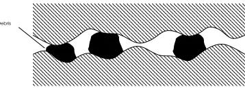
Non-volatile debris left after the evaporation of rinsing liquid, during the final release step for micromachines, can act as an adhesive enhancer when surfaces are in close proximity, as shown in Figure 2.2 [47].
Chapter 2. PRELIMINARIES 17
Debris
Figure 2.2: Debris remaining between microstructure surfaces may enhance the adhesion.
2.1.3
Van der Waal’s force
This force exist due to the interaction between instantaneous dipole moments. However, such inter-action is retarded for large separation, approximately 20 nm [47]. Therefore, van der Waal’s force can be thought , since vertical gaps in MEMS are much larger than 20 nm, to have similar effect as that of solid debris.
Van der Waal’s force can be estimated using the following relation [58]:
LvdW =−
HA
6πh3. (2.2)
2.1.4
Electrostatic forces
Charges are known to accumulate from the ambient and migrate across insulating surfaces on silicon chips [58]. Also, electrostatic force arises on such charged surfaces due to externally applied voltage across the interface and differences in the material work function of the surfaces [47].
In IC industry, such surface charges were the source for device instability. This was solved by thickening the oxide and nitride insulating layers. Polysilicon, as well, can be passivated with self-assembled monolayer films anchored on the surface oxide [58].
The electrostatic forces can be calculated using the relation for parallel-plate capacitor:
Lei=−
U2A
2h2 . (2.3)
2.1.5
Hydrogen bonding
For a fully hydrated silica surface, the density of hydrogen bonding sites was found to be 5 per nm2.
This will yield, approximately, 200 mJ/m2 adhesion energy [58]. The same authors reported that
2.1.6
Asperity deformation force
This is a repulsive force that arises due to non-uniform surface topography, i.e., due to surface roughness. If contact between two surfaces occurs, the highest peaks of the surface will react with a repulsive force, due to its elasticity. The magnitude of this force depends on the surface height distribution function, the mechanical properties of the contacting solid, and the asperity interference that depends on the normal load [47]. See Figure 2.3.
Figure 2.3: Equivalent contact model of two rough surfaces [47].
Figure 2.4 shows a plot of the three attractive forces, neglecting hydrogen bonding, as a function of the vertical separation. From the figure it can be seen that capillary forces dominate at larger separation ranges, about two order of magnitude larger than electrostatic force. Also, it should be noted that the magnitude of electrostatic and van der Waals forces become significant when the two surfaces are near contact.
To prevent such forces from causing bending and stiction in the structure, it must be treated to reduce the magnitude these forces below the spring-restoring forces of the device material, normally silicon. Techniques for reducing these forces include the removal of hydrophilic groups, making the surface more conductive, and decreasing the actual contact area between the two surfaces by increasing roughness. The minimum (or critical) micromachine stiffness to prevent stiction was given by Komvopoulus [47] as:
k∗
=−dLmax
−h∗ (2.4)
whereLmaxis the magnitude of maximum attractive force,dis the stand free separation between the
suspended microstructure and the substrate, andh∗
is the surface separation distance corresponding to the maximum attractive force.
2.2
Adhesion Under Capillary Forces
Chapter 2. PRELIMINARIES 19
Figure 2.4: Comparison of attractive forces per 1 mm2 area existing at the dimensions of
mi-crostructures as a function of the separation between two perfectly smooth surfaces of silicon [58].
in order to maximize the transducer capacitance [65]. This structure, under certain conditions, can collapse and adhere to its underlying substrates.
When a liquid is in contact with a solid, it will exert certain pressure, given by Young’s equa-tion (2.1). The resulting angle at the interface can be found from:
γLS=γSV −γLV cosθ (2.5)
at equilibrium. Here, γ represents the surface tension for the subscripted system, i.e., solid (S), liquid (L), and vapor (V), andθis the contact angle. This is shown in Figure 2.5. When the system satisfy the criterion γLA−γSL < γSA it is energetically favorable for the liquid to spread on the
surface of the solid.
For the case of two parallel plates with a drop of liquid forming a bridge trapped between them, the surface energy stored , neglecting liquid-vapor interaction (since its area is much smaller than that for liquid-solid or solid-vapor) is given by:
Figure 2.5: Contact angle relation with wettability
And, using Young’s equation (2.5):
Us= 2π[r2oγSA+γLAr2l cosθ]. (2.7)
The force required for moving the plate small distance,dz, will be:
F =− dUdzs
!
(2.8)
which, realizing that the volume of trapped liquid is constant, can be combined with (2.7) to give:
F=−2πγlcosθr
2
l
z. (2.9)
The capillary pressure,q, will be:
q=F
A =−2πγl cosθ
z . (2.10)
A spring can be added to the system to represent the elasticity stored in the structure, Figure 2.6.
Figure 2.6: Schematic of spring-rigid plate-liquid system. The structure is pulled toward the substrate as the liquid vanishes [65].
Chapter 2. PRELIMINARIES 21
fluid before it overflows,V◦, will beπr◦2h. For this case, the surface energy stored will be:
Us=
(
Us◦+ 2πγlcosθ
r2 ◦− Vl πz
z≥z∗
Us◦+ 2πγl(1−cosθ)
r2 ◦− Vl πz
z≤z∗ (2.11)
whereUs◦is a constant, andz ∗
= Vl
πr2
◦
.
The total energy of the system, neglecting the plate weight, is:
UT =US+UE=Us◦+ 2πγlcosθ(r◦2− Vl
πz) + 1
2k(h−z)
2 (2.12)
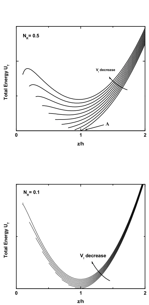
where UE is the elastic energy from spring. Figure 2.2 shows the total energy for different liquid
volumes. The curve has one or two minima. One minimum occurs at the break point of Us,
implying that an equilibrium liquid radius isr◦. The other minimum results when dUT
dz = 0 or, from
equation (2.12):
z2(z−h) +2γlcosθVl
k = 0. (2.13)
These two minima can be written as:
β∞:ξ=λ
β:ξ=Nc(1−λ)λ2
(2.14)
whereξ= Vl
V◦,λ=
z
h, andNc= kh2
2πγlcosθr2◦
.
The two minima,β∞andβ, will intersect if the equation:
ξ= 1 2 ± 1 4 − 1 N◦ 2 (2.15)
has real roots. Therefore, ifNc<4 the two curves will not intersect. This value,Nc= 4, is denoted
asNT. A new quantity is then defined asNEC= NNT◦, and is calledelastocapillary number. The new
number will have a threshold value at 1; ifNEC <1 the two curves will not intersect.
The above analysis is useful in determining weather the suspended structure will bend under capillary force to an extent it touchs the underlying substrate or not. To clarify this, Figure 2.2 shows the total surface energy versus vertical spacing for different liquid volumes. If we start at point A, wherez=h(spring relaxed), and then start the evaporation, the trajectory followed will be that of minimum possible energy. However, since the curves have more than one local minimum, the trajectory will be also dependent on the parameterNc(i.e.,k,h,γ, andθ). Figure 2.2 shows the
paths that will be followed by the system for two differentNcvalues during the evaporation process.
Figure 2.7: Change in total energy (UT) as a function of vertical separation () for entrapped liquid
Chapter 2. PRELIMINARIES 23
dependence can be derived by adding the three energy components (i.e., elastic, S-L interface, and S-S adhesion energies). The relations are [28, 66]:
UE= EI
2 Z l/2
−l/2
∂2u ∂x2
dx (2.16)
USL=−4γlwcosθ(xl−xs) (2.17)
USS =−2γswxs (2.18)
whereUE is the elastic energy,E is the Young’s modulus,I is the moment of inertia of the beam,
USL is the solid-liquid surface energy,USS is the solid-solid adhesion energy, and x,xl, xs,wandu
are as shown in Figure 2.9.
Figure 2.9: Cross section of a doubly clamped beam adhering to its substrate [66].
Taking the sum off these three quantities will give the total energy of the system. Minimizing the total energy with respect to the lateral dimension,x, gives the following parameter [28, 66]:
Np=k
EH3t3
γsl4
(2.19)
wherekis a constant that depends on the geometry of the system,e.g., k= 128/5 for circular disk and 3/8 for suspended beam. Np is defined as thepeel number. ForNp>1 the structure will peel,
otherwise, it will adhere.
As seen in equation (2.19), new system parameters are now playing role in determining its final state, those are:E (Young’s modulus),t(structure thickness), andγs(interfacial adhesion energy).
Recall, from section (2.1) in this chapter, that number of forces affect the adhesion process. Such effects have to be taken into consideration. It is possible to do so either by introducing unique relations for each force,e.g., solid bridging effect on adhesion or van der Waal’s interaction forces, or, possibly, their effect can be lumped with other system parameters presented above,e.g., solid bridging effect can be lumped withγs, asperity deformation withE and so on. Such analysis was
Chapter 2. PRELIMINARIES 25
2.3
Current Stiction Solutions
Many attempts were made during the last few years to deal with the problem of stiction. The problem was studied from different approaches. Those approaches can be divided into three major categories. The first category is where a modification is introduced to the fabrication process itself in order to eliminate the surface forces that cause stiction. The second category includes the methods in which surface topography or structure was altered. The final category is that treated the surface to reduce its energy by depositing a self-assembled monolayer. These three categories are discussed next.
2.3.1
Process modification
The major cause of stiction in microstructure, as discussed, is the capillary forces that arise during the release of final structure. The liquid-vapor transition during release is the cause for such phenomenon. Therefore, attempts were made to avoid such transition,i.e., liquid-vapor transition, to eliminate the origin of the problem.
Before discussing the techniques under this category, it is useful to mention some of the slight modification that was made to the release process. Originally, after the devices were etched with HF, de-ionized water was introduced to replace the etching solution and to remove etching debris. The water was then evaporated to get the final product [60]. Since silicon and other silicon compounds are hydrophilic materials, this process involved high capillary forces. Methanol was then used to wash the de-ionized water and replace it before evaporation. Methanol has a lower surface tension compared to water, 22.65 versus 72.88 mNm−1 [40]. Although better results were obtained by this
method compared to water, the problem was not solved.
Freeze (Sublimation) drying
The liquid-vapor phase change is avoided here by first freezing the liquid, then subliming it to get the free structure. This method first appeared in 1989 [64]. In this method, a mixture of water and methanol,t-butylalcohol, orp-dichlorobenzen were used for sublimation [40, 64].
Supercritical drying
In this technique, the rinsing water is gradually replaced by liquid CO2at elevated pressures inside
a high-pressure chamber. The sample is then taken to the supercritical point of CO2 where the
liquid-gas interphase is avoided.
This is a very successful technique for eliminating release stiction, with nearly 100% yields [63]. Also, commercial large scale supercritical dryers are now available [64], which is another advantage of the technique. However, two disadvantages present here. First, the process involves very high pressure (72 atm [64]) which requires additional safety precautions. Second, is the need for a complicated setup, in the price range, for small scale dryers, of $10,000 - 100,000 [4].
Vapor phase Etching
Etching using vapor phase mixture of HF/H2O was introduced in 1966 [50]. In this technique, vapor
mixture of HF/H2O is introduced in a chamber, where the structure is at relatively high temperatures
(80◦
C). This is to prevent water condensation from the reaction mixture. The pressure of HF can be controlled which will affect the etching rate.
Lee et al. [50] replaced the water in the etching mixture with methanol. This was done to avoid condensation of water during the reaction which may produce capillary forces. Yet, another modification was made by Cole et al. [16] to overcome the low etching rates in gas phase etching, compared to liquid HF. Cole and his coworkers combined both techniques, dry and wet, so that the bulk of the sacrificial structure will be quickly removed by wet etching, followed by dry process to complete the etching.
Xenon difluoride (XeF2) is another gas phase etchant. Whereas HF is used for silicon dioxide
etching, XeF2 is used for silicon etching [14].
Dry etching has the advantages of simplifying the etching process; no additional solutions are needed, better small-geometry penetration, and high selectivity. On the other hand, etching rates are slower than the wet processes, and it requires a batch process to control the pressure.
Table 2.3.1 presents a summary of different etching techniques [40].
2.3.2
Surface modification techniques
Since surface forces are the cause of stiction, it is, intuitively, expected that smaller contact areas will give lower forces. To reduce the contact area of a surface, it can be textured to generate rough interface. Indeed this method increased the detachment length by a factor of two. Another way to reduce the contact is to construct a periodic array of small supporting posts called dimples [64].
C h a p te r 2 . P R E L IM IN A R IE S 2 7 Release meth-ods
Evaporation drying Sublimation drying Supercriti-cal Drying
HF VPE SAM Coat-ings
Procedure HF→DI HF →DI
→methanol
HF →DI
→methanol
HF →DI
→methanol
→ p-dichloro-benzene
HF →DI
→methanol
→CO2
HF vapor HF →DI
→H2O2
→IPA
→CCl4
→OTS
→IPA→DI
Melting T (◦
C) 0 -97.5 26 56 -56.4 -83.2 N/A
Boiling T (◦
C) 100 64.7 82.2 173 -78.3 20 N/A
Vapor Pressure (torr)
17.54 @ 20◦
C 140 @ 27◦
C 27 @ 20◦
C 1.03 @ 25◦
C N/A 687.8 @◦
C N/A
355.2 @ 80◦
C 10 @ 54.8◦
C
Surface Ten-sion (mN·m−2)
72.88 @ 25◦
C 22.65 20.17 N/A 1.16 N/A N/A
Advantages Simple Lower sur-face tension
than DI
water
Fast subli-mation
Only hot plate needed
Clean No liquid in-volved No com-plicated setup Excellent re-sults Excellent re-sults Excellent re-sults
Disadvantages Medicore re-sults Medicore re-sults Requires refrigera-tion and vacuum Toxic Complicated setup Complicated setup Many chemi-cal and rins-ing steps
Absorbs water
Needs vacuum Under
devel-opment Contracts upon
solidifying
of microstructures. They utilized the different oxidation rates between grain boundaries and grain for heavily doped n-type silicon. The process consists of two steps. First, the silicon is doped with phosphorous before being thermally oxidized. This oxide layer is etched, and only the thick layer over grain boundaries remains. Second, the polysilicon is etched to make the grain holes; the remaining oxide acts as a mask for polysilicon.
Another process was proposed by Fujitshka and Sakata [25] where a silicon substrate with low resistivity, underneath a SOI layer, is etched to increase its roughness. Three features of this work were mentioned, those are roughening of substrate, formation of asperities, and increment of gap between SOI and substrate.
Surface texturing has two major drawbacks. First, it cannot be applied to all systems, because some structures require a flat surface for operation (e.g., transducers). Second, dimples adhere stronger than expected by force relation to surface area and surface tension, which is believed to be due to the formation of solid bridge of SiO2 as the water evaporates [64].
2.3.3
Surface energy reduction by organic monolayers
Applying ultra-thin organic films to solid substrate allows tweaking its characteristics [78], e.g., insulation or hydrophobicity. Such layers have very small thickness of an order of tens of angstroms. This is very advantageous in microelectronics, because the structures of the devices will have a thickness and spacing between different parts in the order of few microns. Therefore, the structure may be affected if thick films were deposited.
In addition to their small thickness, two other features give self-assembled monolayers (SAM’s) the expected potential for being a possible solution for stiction. First, the deposition of SAM’s is relatively simple, compared to other films,e.g., polycrystalline diamond [27]. Simply, a monolayer can be deposited from a suitable solution in few minutes at normal temperatures and pressures. The second feature, and of most importance, is the fact that SAM can handle both release and in-use stiction. This last characteristic is a unique feature for SAM’s and no other technique succeeded in doing so without, or at least with slight, effect on the structure.
Silanes and flourosilanes show superior properties in terms of reducing the surface energy of silicon substrates [90]. Contact angles for water on silicon were largely increased when such films were deposited, and surface energy drops by 2 to 7 times that of bare silicon [90].
Alkene based monolayers show superior results in reducing surface energy. Compared to silanes, it has the advantage of being more robustly applied, but the deposition process involves heating at high temperatures (180◦
Chapter 2. PRELIMINARIES 29
2.4
Self-Assembled Monolayers (SAM)
Self-assembled monolayers (SAM’s) are molecular assemblies that are formed spontaneously by the immersion of an appropriate substrate into a solution of an active surfactant in an organic sol-vent [97].
A self-assembling molecule can be divided into three parts, form energetic point of view [97], head, backbone, and tail, Figure 2.4. The head group-substrate pair is used to define the individual SAM system [85].
Figure 2.10: Schematic of SAM. Shaded circle indicates chemisorbing headgroup and open circle endgroup, which can be chosen from variety of chemical functionalities [85].
To define a SAM structure, two features need to be determined [85]:
1. The 2D-structure of the molecules, i.e., their layout, with respect to the substrate. This is done using a convention of SAM film molecule orientation with respect to the substrate, as shown in Figure 2.4.
2. The 3D-structure of the molecular backbones which includes a possible tilt angle with respect to surface normal, the tilt direction, the twist angle, etc. Figure 2.4.
It is important to note, however, that not all SAM’s show crystallinity, therefore, the 2D structure may be amorphous.
2.4.1
SAM’s characterization techniques
Wide rang of analytical tools are used to study SAM’s. In general, the analysis aims to determine the structure of molecules, i.e., chemical, electrical potential, etc., or to determine geometrical orientation, 2- and 3-D structures. A brief description of the most common techniques follows.
Ellipsometry
Chapter 2. PRELIMINARIES 31
Figure 2.12: Schematic of angular degrees of freedom of alkanethiol (bound to substrate via thiol group, with alkyl chain fully stretched). Angle θt refers to tilt of molecular axis with respect to
substrate surface normal. χt defines tilt direction, i.e., it is derived from projection of molecule
in substrate plane. χt is undefined for θt = 0. Twist angle, ψ, describes rotation about axis of
wave components. The phase shift between the two components, using certain value for the refractive index, is then translated into thickness spectroscopy [95].
Microscopy techniques
This category includes,e.g., surface tunneling microscopy (STM), atomic force microscopy (AFM), and scanning electron microscopy (SEM). The strength of such techniques is to provide a direct image of the structure [85].
Different information can be obtained using this technique. Besides probing the surface topogra-phy, AFM for example, can be used to probe the electrical conductivity or chemistry of the surface.
Diffraction based techniques
Diffraction techniques are used to study the 2D structure of SAM’s. It includes low-energy electron diffraction (LEED), grazing incidence x-ray diffraction (GIXD), and low-energy atom diffraction (LEAD).
Spectroscopy based techniques
This includes infrared techniques,e.g., SFG and NXAFS, in which the waves interact with transient dipole which allow drawing conclusion on the structure.
X-ray photoelectron spectroscopy operates at high energy levels that can penetrate deeper in the SAM, allowing the study of binding energy of the head groups.
Spatially averaging techniques
Techniques in this category works on average of a relatively large scale, enough to insure actual representation of the sample. However, such techniques do not give a detailed view of the structure. Contact angle measurements are one simple technique to measure surface energies and wetting behavior. Quartz Crystal Microbalance (QCM) is another example on this category.
2.4.2
Merits of SAM’s
Chapter 2. PRELIMINARIES 33
1. Unusual chemical and electrical stabilities.
2. Degree of perfection in terms of molecular density, packing, and orientation.
3. Monolayers can be prepared from chemisorbed, physisorbed, or combination of both molecules. 4. Molecules are attached to the surface (e.g., via covalent bonds) and it is intralayer polymerized. Therefore, SAM’s can, in principle, be formed on top of a solid surface which can then be sepa-rated from the monolayer. This will yield a true 2D surface of one molecule width. In addition, the formed layer will epitaxial transfer information from a molecularly organized solid surface [73, 74]. As a result, from research point of view, SAM’s offer unique opportunities to increase fundamental un-derstanding of self-organization, structure-properties relationships, and interfacial phenomena [99].
From a practical point of view, SAM’s have the following unique characteristics [85]: 1. Ease of preparation.
2. Tunability of surface properties via modifications of molecular structure and functional groups. 3. The use of SAM’s as a building blocks to more complex structures,e.g., multilayer building. 4. The possibility of lateral structuring in the nanometer regime.
5. The applications made possible by these features.
2.4.3
Common SAM systems
Several systems have been used to form SAM’s. Among those, SAM systems of thiol (sulfur con-taining organic compounds) on Au(111) [85] surface are probably the most popular. Organosilicon SAM’s on silicon substrate, or silicon dioxide, is another example of well studied systems. These two systems will be discussed next.
Thiol/Au systems
This is probably the most studied and understood among SAM systems. This is due to the ease of preparation and well-defined order, plus the inertness of the substrate, gold [85]. While thiols SAM can be formed on several metals,e.g., silver, copper, mercury, GeAs, and InP, gold is preferable due to its resistance to oxidation in air, which have made gold substrates convenient and reproducible for laboratory experiments [98].
different surface properties. For example, a high surface energy may be produced with a CO2H
group, lower energies can be obtained using OCH3, and, yet lower energies are obtained with CH3
terminating group [98].
The most important factor in thiol deposition is the gold substrate condition. The contaminates on the gold surface are known to cause large variations in its wettability [89]. These contaminations are generally carbonaceous materials, and techniques like UV/O3or oxygen plasma are a common
methods to remove these contaminations. However, such techniques cause the formation of oxidized surface which cause a systematic variation of the formed layer [83].
The preparation of thiol SAM’s is usually done from liquid solutions of, typically, 1 mM concen-tration. Ethanol is most commonly used for this purpose. Other solvents include hexane, cyclohex-ane [98], and water [83]. Contact angle measurements, however, showed a dependence on the used solvent [83].
The mechanism of thiol adsorption starts either by ionic dissociation of thiols or by the formation of H•
, according to the following reactions [98]:
RSH + Au
RSAu−
+ H2 (2.20)
RSH + Au
RSAu + H•
(2.21) While desorption takes place according to one of the following schemes:
2RSH+2Auka
kd
2RSAu + H2 (2.22)
RSH + Auka
kd
RSSR+2Au. (2.23)
The hydrogen in reaction (2.22) is generated by the association of two hydrogen radicals generated in reaction (2.21).
The increase in the system order, due to molecular organization to form the SAM, will be surpassed by a negative change in enthalpy, making the total Gibbs energy (∆G) negative, indicating a spontaneous process. The situation is reversed for the desorption reactions (2.20) and (2.21), with higher energy barrier for disulfide formation than that for thiols. Therefore, it is more probable for the desorped molecules to be converted back into thiol molecules than disulfide. The over all SAM formation reaction will be [98]:
RSH(solv)+ Au(s)
ka kd
RSAu(s)+
1
2H2(solv) (2.24)
Chapter 2. PRELIMINARIES 35
With respect to adsorption kinetics, it is believed that the adsorption takes place in two distinct steps. The first step is a very fast step, which lasts a few minutes, by the end of which the layer will have a contact angles close to their limiting values and a thickness of about 80-90% of its maximum. The second step is a slow step which lasts several hours, at the end of which the thinkness and contact angles reach thier final values [99]. The first step is well described by the Langmuir adsorbtion isotherm:
dθ
dt =ka(1−θ)C−kdθ (2.25)
where θ is the fraction of occupied sites, and ka and kd are the adsorption and desorption rate
constants, respectively.
The structure of the formed SAM on Au(111) surface1was studied using electron diffraction
tech-nique. The structure is believed to be a hexagonal with a S· · ·S spacing of 4.97 ˚A per molecule [99]. However, other crystallinties were recently observed, namely, the dense (√3×√3) packing. The packing of molecules strongly depends on the surface morphology of the substrate and the end group of the thiol molecules [85].
2.4.4
Organosilicon SAM’s
Different silicon containing organic compounds,silanes, have been deposited on many hydroxylated surfaces. Alkylchlorosilanes, alkylalkoxysilanes, and alkylaminosilanes are examples of deposited compounds. Substrates on which the layers were formed include silicon oxide, aluminum oxide, quartz, glass, mica, zinc selenide, germanium oxide, and gold [99].
Alkylchlorosilane compounds have been receiving increasing attention because of thier superior performance in reducing stiction problem and surface energy for silicon based materials [57, 39]. This project emphasizes the potential anti-stiction coatings for MEMS devices, therefore, alkylchlorosilane SAM’s on Si substrates will be discussed in more details.
Alkylchlorosilanes
Octadecyltrichlorosilane (CH3(CH2)17SiCl3,OTS) is perhaps the most common anti-stiction agent
that is currently being studied. When properly applied, OTS can achieve the following characteris-tics [57]:
1. Eliminate release stiction by effectively reversing the shape of the water meniscus.
2. Reduce in-use stiction by three to four order of magnitudes
1This morphology is commonly used for thiol deposition experiments because it is the most stable among different
3. Eliminate the need for large input signals in the start-up phase. 4. Reduce friction in microengines.
5. Reduce wear significantly.
However, since OTS has three chlorine atoms in the head group, it is highly sensitive to water; the main draw back for OTS [99].
Another trichlorosilane used is 1H,1H,2H,2H-perfluorodecyltrichlorosilane (CF3(CF2)7(CH2)2
-SiCl3, FDTS). This is the most effective reagent to prodcue hydrophopic coating on oxide-coated
surfaces [90]. The surface tension of a FDTS coated substrate is about 4 times lower than surfaces coated with OTS, and 2.5 times lower than Teflon. However, FDTS is extremely sensitive to moisture and must be handled and stored under inert atmosphere,e.g., N2 [90].
Cholorsilanes with two chlorine atoms have been recently studied as a potential anti-stiction coat-ing for silicon surfaces. With two chlorine atoms, there is an improved control over polymerization. Example for such material is dichlorodimethylsilane (DDMS) [39].
OTS SAM formation process
Since OTS is sensitive to water, the process to apply such material is quite challenging. While the presence of water in the solution may cause the OTS molecules to polymerize, forming siloxane groups, very small amount of water are required for the reaction to take place. The necessary amount of water is not exactly known, however, a value of 0.15 mg water per 100 ml solution was suggested [99].
Different deposition techniques are used to form the OTS SAM. Commonly, adsorption of OTS molecules from a liquid solution onto silicon substrates is used. In addition, gas phase deposition has also been done, as well as deposition from liquid CO2[21]. For MEMS release, it is only feasible
to apply the film from a liquid solution, therefore, this technique will be discussed here.
The deposition process is usually carried out in a mixture of hexadecane and chloroform solution (4:1 V/V). Chloroform acts as a cosolvent to increase the solubility of chlorine head [9], carbon tetra-chlide my also be used for this purpose in place of chloroform. Other solvents, beside hexadecane, are used, those include toluene [5] and bicyclohexyl [87].
The immersion time for OTS monolayer preparation varies among different research groups. Intervals of 1 minute and up to 1 hour had been employed, but usually 10 to 15 minutes [87, 90].

![Figure 1.2: Schematic representation of a generalized chemically amplified resist process [60].](https://thumb-us.123doks.com/thumbv2/123dok_us/1722283.1219532/15.595.69.470.231.569/figure-schematic-representation-generalized-chemically-amplied-resist-process.webp)

![Figure 1.4: Examples of MEMS devices produces by Sandia National Laboratories (a,b,c) [49] andTexas Instruments (d) [34].](https://thumb-us.123doks.com/thumbv2/123dok_us/1722283.1219532/23.595.148.449.214.490/figure-examples-devices-produces-national-laboratories-andtexas-instruments.webp)
![Figure 2.2 [47].](https://thumb-us.123doks.com/thumbv2/123dok_us/1722283.1219532/26.595.225.375.222.296/figure.webp)

![Figure 2.9: Cross section of a doubly clamped beam adhering to its substrate [66].](https://thumb-us.123doks.com/thumbv2/123dok_us/1722283.1219532/34.595.201.397.316.419/figure-cross-section-doubly-clamped-beam-adhering-substrate.webp)

