Western University Western University
Scholarship@Western
Scholarship@Western
Electronic Thesis and Dissertation Repository
8-29-2012 12:00 AM
A Control Scheme for an AC-DC Single-Stage Buck-Boost PFC
A Control Scheme for an AC-DC Single-Stage Buck-Boost PFC
Converter with Improved Output Ripple Reduction
Converter with Improved Output Ripple Reduction
Kamran Rezaei
The University of Western Ontario
Supervisor
Dr. Gerry Moschopoulos
The University of Western Ontario
Graduate Program in Electrical and Computer Engineering
A thesis submitted in partial fulfillment of the requirements for the degree in Master of Engineering Science
© Kamran Rezaei 2012
Follow this and additional works at: https://ir.lib.uwo.ca/etd
Part of the Power and Energy Commons
Recommended Citation Recommended Citation
Rezaei, Kamran, "A Control Scheme for an AC-DC Single-Stage Buck-Boost PFC Converter with Improved Output Ripple Reduction" (2012). Electronic Thesis and Dissertation Repository. 813.
https://ir.lib.uwo.ca/etd/813
This Dissertation/Thesis is brought to you for free and open access by Scholarship@Western. It has been accepted for inclusion in Electronic Thesis and Dissertation Repository by an authorized administrator of
A Control Scheme for an AC-DC Single-Stage Buck-Boost PFC Converter
with Improved Output Ripple Reduction
(Spine Title: A New Control Scheme for Single-Stage PFC Converters)
(Thesis format: Monograph)
by
Kamran Rezaei
Faculty of Engineering
Department of Electrical and Computer Engineering
Graduate Program in Engineering Science
A thesis submitted in partial fulfillment
of the requirements for the degree of
Master of Engineering Science
The School of Graduate and Postdoctoral Studies
The University of Western Ontario
London, Ontario, Canada
ii
THE UNIVERSITY OF WESTERN ONTARIO
SCHOOL OF GRADUATE AND POSTDOCTORAL STUDIES
CERTIFICATE OF EXAMINATION
Supervisor
______________________________
Dr. Gerry Moschopoulos
Examiners
______________________________
Dr. Ken McIsaac
______________________________
Dr. Anestis Dounavis
______________________________
Dr. Brian Pagenkopf
The thesis by
Kamran Rezaei
entitled:
A Control Scheme for an AC-DC Single-Stage Buck-Boost PFC Converter
with Improved Output Ripple Reduction
is accepted in partial fulfilment of the
requirements for the degree of
Master of Engineering Science
Date__________________________ _______________________________
iii
ABSTRACT
AC-DC power factor correction (PFC) single-stage converters are attractive because of their cost
and their simplicity. In these converters, both PFC and power conversion are done at the same
time using a single converter that regulates the output. Since they have only a single controller,
these converters operate with an intermediate transformer primary-side DC bus voltage that is
unregulated and is dependent on the converters’ operating conditions and component values.
This means that the DC bus voltage can vary significantly as line and load conditions are
changed. Such a variable DC bus voltage makes it difficult to optimally design the converter
transformer as well as the DC bus capacitor.
One previously proposed single-stage AC-DC converter, the Single-Stage Buck-Boost Direct
Energy Transfer (SSBBDET) converter has a clamping mechanism that can clamp the DC bus
voltage to a pre-set limit. The clamping mechanism, however, superimposes a low frequency 120
Hz AC component on the output DC voltage so that some means must be taken to reduce this
component. These means, however, make the converter transient slow and sluggish.
The main objective of this thesis is to minimize the 120 Hz output ripple component and to
improve the dynamic response of the SSBBDET converter by using a new control scheme. In the
thesis, the operation of the SSBBDET converter is reviewed and the proposed control method is
introduced and explained in detail. Key design considerations for the design of the converter
controller are discussed and the converter’s ability to operate with fixed DC bus voltage, low
output ripple and fast dynamic response is confirmed with experimental results obtained from a
prototype converter.
Keywords: AC-DC power conversion, Power Factor Correction (PFC), Single-stage converter,
iv
Dedication
With all my heart to my precious family and friends who gave me unconditional
v
Acknowledgments
I would like to thank my supervisor, Dr. Gerry Moschopoulos, for giving me the opportunity to
join and collaborate with his research group during past two years. The accomplishments of this
research would not have been achieved without his extensive support, encouragements and
guidance.
I also would like to thank my colleagues at Dr. Moschopoulos’s laboratory especially Mr. Navid
Golbon who helped me with all aspects of my work and providing such a friendly environment
vi
Table of Contents
CERTIFICATE OF EXAMINATION ... ii
ABSTRACT ... iii
Dedication ... iv
Acknowledgments ... v
Table of Contents ... vi
List of Figures ... ix
List of Appendices ... xi
List of Acronyms and Abbreviations ... xii
1. Introduction ... 1
1.1. Power Electronics ... 1
1.2. Power Factor and Harmonic Distortion ... 2
1.2.1. Standards, Regulations and Limitations for Harmonic Distortion in a Power Converter ... 3
1.3. Power Factor Correction (PFC) ... 3
1.3.1. Active Approaches for Power Factor Correction ... 4
1.4. Single-Stage Active PFC Techniques ... 5
1.4.1. Single-Stage Converters with Variable Switching Frequency ... 6
1.4.2. Single-Stage Converters with Voltage Feedback Techniques ... 7
1.4.3. Single-Stage Converters with Direct Energy Transfer ... 8
1.5. Control Approaches for Single-Stage PFC AC/DC Converters... 9
1.5.1. Peak Current Mode Control ... 9
1.5.2. Hysteresis Current Control ... 11
1.5.3. Average Current-Mode Control ... 11
1.6. Thesis Objectives ... 12
vii
2. A Low-Power AC-DC Single-Stage Converter with Reduced DC Bus Voltage Variation
Using Direct Energy Transfer Technique... 15
2.1. Introduction ... 15
2.2. Converter Operating Principles and Modes of Operation ... 15
2.3. Steady-State Analysis and Converter Design ... 19
2.4. Conclusion ... 24
3. Averaged State-Space Modeling and Small-Signal Analysis of the Single-Stage PFC Converter ... 25
3.1. Introduction ... 25
3.2. Averaged State-Space Modeling of PWM Converters with One Inductor Operating in DCM .. 26
3.3. Averaged State-Space Modeling of the Single-Stage PFC AC/DC Converter with Direct Energy Transfer ... 29
3.4. Conclusion ... 36
4. New Control Scheme for Single-Stage PFC AC/DC Converters Employing Direct Energy Transfer ... 38
4.1. Introduction ... 38
4.2. Limitation of Conventional Average Current-Mode Control Structure for the Proposed Single-Stage PFC Converter ... 38
4.3. A Control Strategy for the Single-Stage PFC Converter with Direct Energy Transfer ... 40
4.4. Conclusion ... 52
5. Experimental Results of the Single-Stage PFC AC/DC Converter with Proposed Control Scheme ... 53
5.1. Introduction ... 53
5.2. Experimental Results of the Implemented Single-Stage PFC Converter ... 53
5.2.1. Input Current Waveforms and Harmonic Content ... 55
5.2.2. Output Voltage, Transient Response and Efficiency ... 57
5.3. Conclusion ... 58
viii
6.1. Introduction ... 59
6.2. Summary ... 59
6.3. Conclusions ... 62
6.4. Contributions ... 63
6.5. Proposal for future work ... 64
Appendix A ... 65
References ... 67
ix
List of Figures
Fig. 1.1 Passive PFC with the filter on (a) the AC side, (b) the DC side of the diode bridge….…3
Fig. 1.2 Two-stage AC/DC PFC converter………..4
Fig. 1.3 Popular IHQRR single-stage PFC converters, (a) BIBRED, (b) BIFRED………6
Fig. 1.4 (a) boost/single-switch flyback converter (b) DC bus voltage feedback in S2IP2 converters……….7
Fig. 1.5 Parallel PFC power processing diagram……….8
Fig. 1.6 Buck-boost single-stage PFC with direct energy transfer………..8
Fig. 1.7 Peak current control scheme on a boost PFC converter [42]……….9
Fig. 1.8 Hysteresis current control on a boost PFC converter [42]………....10
Fig. 1.9 Average current mode control on a boost PFC converter [42]……….…12
Fig. 2.1 Proposed buck-boost single-stage PFC with direct energy transfer……….…16
Fig. 2.2 Typical converter waveforms describing single flyback transformer mode………17
Fig. 2.3 Equivalent circuits in single flyback transformer mode (a) Interval I (b) Interval II…...17
Fig. 2.4 Typical converter waveforms describing dual flyback transformer mode…………..….18
Fig. 2.5 Equivalent circuits in dual flyback transformer mode (a) Interval I (b) Interval II…...18
Fig. 3.1 DC/DC Boost Converter………...26
Fig. 3.2 Time intervals of inductor current in a DCM operating converter………...27
Fig. 3.3 Magnetizing inductances current waveforms……….…..30
Fig. 4.1 Single-stage PFC converter with conventional average current-mode control……...….39
Fig. 4.2 Proposed control strategy on the single-stage PFC converter………..42
x
Fig. 4.4 Relative Output voltage ripple amplitude for different designs of PFC converter……...49
Fig. 4.5 Designed control scheme for the single-stage PFC converter employing direct energy transfer………...50
Fig. 4.6 Block diagram of the designed control system……….51
Fig. 5.1. Input voltage and output voltage sensing circuit……….54
Fig. 5.2. Input current sensing circuit………....55
Fig. 5.3 The input current using the proposed control scheme Vin=100 V (t: 120s/div, I: 2A/div)………...56
Fig. 5.4 The input current using the proposed control scheme Vin=230 V (t: 40s/div, I: 2A/div)………...56
Fig. 5.5 Harmonic content of the input current at Vin=100V and EN61000-3-2 limitations….…56 Fig. 5.6 Harmonic content of the input current at Vin=230V and EN61000-3-2 limitations….…56 Fig. 5.7 Output voltage of the single-stage PFC converter with the proposed control scheme at Vin=230 V (t: 100 ms/div, V: 5V/div)……….……….…57
Fig. 5.8 Transient response of the controller with a load change from full load to half load Vin=100V (t: 10ms/div, V: 20V/div)……….…57
xi
List of Appendices
Average Value of the Current Flowing through an Inductor Operating in Discontinuous
xii
List of Acronyms and Abbreviations
AC Alternating Current
BIBRED Boost Integrated with Buck Rectifier/Energy storage/DC-DC
BIFRED Boost Integrated with Flyback Rectifier/Energy storage/DC-DC
CCM Continuous Conduction Mode
DC Direct Current
DCM Discontinuous Conduction Mode
EMI Electro-Magnetic Interference
IEC International Electro-Technician Commission
IHQRR Integrated High-Quality Rectifier-Regulator
PFC Power Factor Correction
PWM Pulse-Width Modulation
S2IP2 Single-Stage Isolated PFC Power
SSBBDET Single-Stage Buck-Boost Direct Energy Transfer
THD Total Harmonic Distortion
1
Chapter 1
Introduction
1.1.
Power Electronics
Power electronics is a field in electrical engineering that deals with converting an available form
of energy from a power source to the form required by a load. A power converter uses
semiconductor devices such as diodes, MOSFETs and IGBTs to achieve this power conversion.
Diodes are uncontrolled switches that turn on and conduct current when they are forward-biased
and turn off when they are reverse-biased; MOSFETs and IGBTs are controlled switches that can
be turned on or off by a switching signal at their gate (i.e. a high gating pulse is the turn-on
command and a low or zero gating pulse is the turn-off command). A power converter can be an
AC/DC converter, DC/DC converter, DC/AC inverter or AC/AC converter depending on the
application. Many types of power sources can be used for these converters, such as AC
single-phase, AC three-single-phase, DC source, battery, solar panel, or an electric generator. This thesis will
focus on low power (< 100 W) single-phase, AC/DC converters.
Some sort of control method is needed to ensure that the output voltage of an AC/DC converter
is regulated to the desired DC voltage. In a closed-loop power converter, a sensing circuit is
responsible to send output voltage values (samples) to a controller circuit so that adjustments can
be made to the power converter; typically this means changing the converter’s duty-cycle. The
term “duty-cycle” (D) refers to the proportion of on-time to the period T of the switch and is
expressed in percent, with 100% as being fully on. It is by controlling the width of the on-time
2
control method is generally referred to as Pulse-Width Modulation (PWM) in the power
electronics literature.
1.2.
Power Factor and Harmonic Distortion
The input power factor of an AC/DC power converter is an important consideration as it is a
measure of how effectively the converter utilizes AC input power. Power factor is defined as the
ratio of the real power flowing to the load to the apparent power in the circuit [1] and can be
expressed as [2]
∑
(1.1)
where and are rms values of the nth harmonic of input current and input voltage,
respectively and is the phase shift between them. Since the input AC voltage can be assumed
to be a pure sinusoid, the product of voltage harmonic terms and current harmonic terms are zero
with the exception of the product of fundamental voltage and current harmonics so that eq. (1.1)
can be simplified to be
(1.2)
where is the rms value of primary component of the input current. As can be seen from
eq. (1.2), if the input current is a pure sine wave, then power factor can be defined as cosine of
the phase angle between input voltage and current waveforms. Power factor can range from zero
to one, with a power factor of one indicating that the input current is a purely sinusoidal
waveform that is in phase with the input AC voltage.
Another term that is used for measuring the power quality of electrical power systems is Total
Harmonic Distortion (THD). THD is defined as the ratio of the square root of the summation of
the square of all non-fundamental harmonics of a waveform to fundamental component of the
same waveform. For a current waveform, particularly the input current of a power electronic
converter, it can be expressed as
√
3
where is the rms value of the nth harmonic of the input current.
1.2.1. Standards, Regulations and Limitations for Harmonic Distortion in a
Power Converter
The presence of non-fundamental input current harmonic components can have a negative
impact on the operation of an AC/DC converter. This is especially true as they do not contribute
to real power being delivered in the load, but they just circulate in the converter and create power
losses, additional component stresses, heat and Electro-Magnetic Interference (EMI); they also
limit the amount of power that can be delivered by the input AC source [2], [7].
The most negative effect that the input current harmonics of a power converter can have,
however, is that they can corrupt the input AC source voltage. Since electrical equipment,
household appliances, consumer electronics, lighting, computers, factory equipment, medical
equipment, etc. – in short, anything that is powered from an AC utility source – has some sort of
power electronic converter interface, and since all these generate input current harmonics that
can be injected into the grid, the AC utility voltage would become distorted (which would
negatively impact the operation of anything powered by it) were it not for the various standards
that regulatory agencies have mandated to limit the input current harmonic content of power
converters. One such regulatory agency is the International Electro-Technician Commission
(IEC), which has produced current harmonic standards such as EN61000-3-2 that are commonly
used to determine whether a particular electrical product can be sold in the marketplace [4]-[6].
1.3.
Power Factor Correction (PFC)
With the exception of low power converters (< 75 W), most AC/DC converters in commercial
products that are powered by the AC utility grid now have some sort of input Power Factor
(a) (b)
Fig. 1.1 Passive PFC with the filter on (a) the AC side, (b) the DC side of the diode bridge.
4
Correction (PFC). Input PFC techniques are needed to shape the input currents of AC/DC
converters so that they have acceptable harmonic contents with their fundamental harmonic
component in phase with the input AC voltage [9].
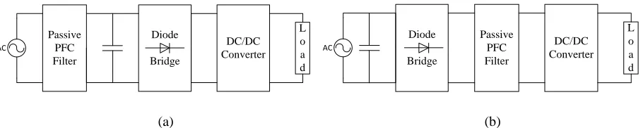
PFC techniques can either be passive or active. Passive techniques use passive elements such as
inductors and capacitors in a low-pass or band-pass filter structure to filter low frequency
harmonics [3]. These passive filters can either be placed at the converter’s input AC side, as
shown in Fig. 1.1(a) or in the intermediate DC link, as shown in Fig. 1.1(b) [10]. Although
passive PFC techniques are simple and inexpensive, they have one significant disadvantage,
which is their need for bulky capacitors and inductors. The size of these elements makes passive
PFC techniques unsuitable for most applications except for low-power applications with narrow
line voltage range.
1.3.1. Active Approaches for Power Factor Correction
Active PFC techniques are much more popular than passive PFC techniques. It is a generally
accepted standard practice to implement a second active converter at the front-end of an AC/DC
converter to perform input power factor correction as shown in Fig. 1.2. In other words, most
AC/DC converters are two-stage converters than consist of an AC/DC front-end converter that
performs PFC followed by a DC/DC converter that converts the output of the front-end converter
into the desired output DC voltage.
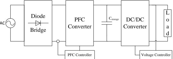
The front-end AC/DC converter has a filter capacitor Cstorage to smooth its output voltage and
make it DC so that it can be fed to the input of the DC/DC converter. AC/DC boost (step-up)
converters are typically used as front-end converters because of their relative simplicity and their
effectiveness in shaping input currents [8]. Flyback and forward converter topologies are
Fig. 1.2 Two-stage AC/DC PFC converter.
Fig. 1.2 Two-stage AC/DC PFC converter. AC
Diode
Bridge
DC/DC Converter
L o a d PFC
Converter
Cstorage
5
typically used as DC/DC converter in applications that are < 200 W, which is the focus of this
thesis. The main drawback of two-stage converters is the cost and complexity that is associated
with operating two separate and independent switch-mode power converters. As a result, power
electronic researchers have been motivated to find alternative approaches to conventional
two-stage AC/DC converters.
1.4.
Single-Stage Active PFC Techniques
Single-stage PFC converters that combine PFC front-end converters and DC/DC converters into
a single converter stage are a cheaper and less sophisticated alternative to conventional two-stage
AC/DC converters [13]-[26]. They are operated with only a single controller to regulate the
output DC voltage as they just have one converter stage, which for low-power applications (<
200 W) has just a single active semiconductor switch (typically a MOSFET). This is in contrast
to conventional two-stage converters that have two controllers – one to regulate the output DC
voltage and the other to regulate the intermediate DC bus voltage that is the input to the DC/DC
converter.
Since single-stage converters do not have a controller to regulate the intermediate DC bus
voltage, this voltage can vary considerably as it is dependent on the input line and output load
conditions. Unless some means is used to limit this voltage, it can reach to levels of up to 1000V
in converters that are operating under high input line and light load conditions. The excessive
level and the variability of the DC bus voltage results in the need for components that can handle
high peak voltage stresses and that can operate under a very wide range of operating conditions.
Single-stage PFC converters can be categorized into the following three distinct types:
1) Single-stage converters with variable switching frequency
2) Single-stage converters with voltage feedback techniques
3) Single-stage converters with direct energy transfer
6
1.4.1. Single-Stage Converters with Variable Switching Frequency
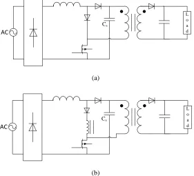
The Integrated High-Quality Rectifier-Regulator (IHQRR) [28] is one of the earliest types of
single-stage AC/DC converters to be proposed. A DCM AC/DC boost converter (Discontinuous
Conduction Mode, where the current of the input inductor reaches zero by the end of each
switching cycle) and a DC/DC converter that operates in CCM (Continuous Conduction Mode,
where the inductor does not discharge completely in any switching cycle) are combined in this
topology. Fig. 1.3 shows an example of a BIFRED (Boost Integrated with Flyback
Rectifier/Energy storage/DC-DC) converter and an example of a BIBRED (Boost Integrated
with Buck Rectifier/Energy storage/DC-DC) converter, which are the most popular
configurations of the IHQRR converter family.
Although the converters in this family operate with a nearly sinusoidal input current, their
components suffer from high voltage stresses. To overcome this issue, the use of variable
switching frequency control in BIFRED and BIBRED converters to reduce the voltage stress on
the storage capacitor Cs was first proposed in [17]. The basic principle is that varying the
converter switching frequency for varying load can affect the energy equilibrium that exists at
the DC bus so that the DC bus voltage can be reduced. Operating with varying switching
frequency can be complicated, however, and it is also difficult to design the converter
components to operate over a very wide range of switching frequencies. (a)
(b)
Fig. 1.3 Popular IHQRR single-stage PFC converters, (a) BIBRED, (b) BIFRED.
7
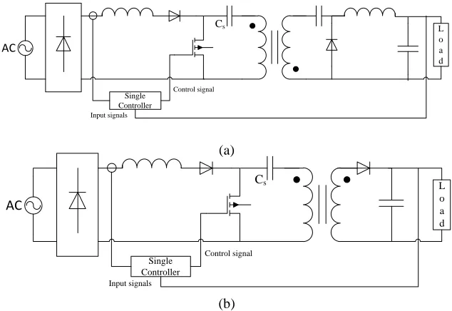
1.4.2. Single-Stage Converters with Voltage Feedback Techniques
To reduce the high voltage stresses on the semiconductor devices in IHQRR type single-stage
converters so-called Single-Stage Isolated PFC Power (S2IP2) converters were proposed by
R.Redl et al. [15, 16]. Fig. 1.4(a) shows the boost/single-switch flyback converter, the most popular topology of this family. The main characteristic of this family is that both the AC/DC
PFC section and DC/DC section operate in DCM. Although S2IP2 converters have a lower DC
bus voltage than IHQRR converters, this voltage can still be greater than 500V.
The DC bus voltage in S2IP2 and IHQRR converters can be reduced if some sort of DC bus
voltage feedback technique is used, as shown in Fig. 1.4(b) [29-31]. In this technique, an
auxiliary feedback winding that is coupled to the transformer is added to the converter. This
winding acts as a negative feedback by preventing the full input voltage from appearing across
the input inductor. Since less energy is stored in the input inductor when the converter switch is
on, less energy is pumped into the DC bus capacitor when the switch is turned off. This affects
the energy equilibrium of the DC bus capacitor so that the DC bus voltage is reduced; this
voltage can be made to be less than 450V, which is considered to be a commonly accepted
voltage due to the size of the DC bus capacitor. Although the DC bus voltage feedback technique
(a)
(b)
Fig. 1.4 (a) boost/single-switch flyback converter (b) DC bus voltage feedback in S2IP2 converters.
AC
L o a d
Cs
AC
L o a d
8
does decrease the DC bus voltage, it introduces distortion in the input AC current around its
zero-crossing regions. This distortion is due to dead-band regions that must exist when the input
voltage is low as no current can flow through the input diode bridge when the input voltage is
less than the voltage across the auxiliary feedback winding.
A load current feedback technique in which an additional winding is added parallel to the
transformer was later proposed in [32]. This technique is based on the same concept as the DC
bus voltage feedback technique, but with a slight difference. This technique directly senses
output power and adjusts input power at different loads, but in the DC bus voltage feedback
technique, the input power is adjusted after DC bus voltage is increased because it feeds back
output power indirectly using the DC bus capacitor voltage.
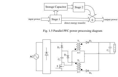
1.4.4. Single-Stage Converters with Direct Energy Transfer
In single-stage AC/DC converters with direct energy transfer, some of the power from the input
source is processed only once in the converter, as shown in Fig. 1.5. As a result, these converters
can operate with higher efficiency than other single-stage converters since some power from the
input is processed only once instead of twice. A number of single-stage converters have been
proposed [33-41] and Fig 1.6 shows a converter of this type that is based on a buck-boost input
Fig. 1.5 Parallel PFC power processing diagram
Fig. 1.6 Buck-boost single-stage PFC with direct energy transfer.
Stage 2
Stage 1 Storage Capacitor
input power
+
output powerdirect energy transfer
9
section that is proposed by N. Golbon et al. in [39]. The difference between the converter shown in Fig. 1.6 and a buck-boost single-stage converter without direct energy transfer is the addition
of a second transformer to the circuit, T1.
The main drawback of single-stage converters with direct energy power transfer is that their cost
and complexity approach those of conventional two-stage AC/DC converters.
1.5.
Control Approaches for Single-Stage PFC AC/DC Converters
The main challenge in operating single-stage PFC converters is the availability of only one
control variable to achieve tight output voltage regulation and sinusoidal-like input current shape
simultaneously. As a result, a tradeoff needs to be considered between output voltage regulation
and input power factor in the design of the controller. Many control techniques have been
designed for single-stage PFC converters [43]-[55]. They can generally be classifed as follows:
1) Peak current control
2) Hysteresis current control
3) Average current-mode control
Each of these control techniques is explained briefly below
1.5.1. Peak Current Mode Control
In peak current control, the positive slope of the input inductor current is controlled to be equal
to a reference value in each switching cycle, regardless of other operating conditions. The switch
10
is turned off when the instantaneous current reaches the reference value. This limit point is
defined based on the output voltage and input current status in each switching cycle. However,
peak current control is inherently unstable when the duty ratio of the converter exceeds 50%. To
stabilize the current feedback loop, a ramp signal (equal to the negative ramp of the input
inductor current in a switching cycle) has to be added to the sensed current signal. This ramp
should be calculated separately for each converter topology, based on circuit parameters and the
output voltage.
Fig 1.7 shows peak current control implemented on a boost PFC front-end AC/DC converter (the
same control scheme can be used for single-stage converters). The sinusoidal current reference is
the product of the voltage compensator output and the sensed input voltage, and it is used to keep
the input current in phase with the input voltage. This forces the voltage feedback loop
compensator to have a low bandwidth so that 120 Hz low frequency ripple in the output voltage
does not distort the input current reference waveform. In this scheme, the main switch is turned
on with a constant frequency at the beginning of the switching cycle and is kept on until the sum
of the sensed input current ramp and external ramp reaches the sinusoidal current reference.
The main advantages of this control scheme are that no current compensator is required for the
controller and the switching frequency is constant. Peak current control, however, suffers from
high sensitivity to noise because any noise spike in the input current can turn the switch off
immediately. Furthermore, at high line and light load conditions where the control scheme is
fully stable, the fixed compensating ramp signal can cause input current distortion.
11
1.5.2. Hysteresis Current Control
This control method was first proposed in [57] and is based on restraining the input inductor
current to be a preset hysteresis band. The switch is turned on when the inductor current goes
below the predefined lower value and is turned off when the inductor current goes above the
upper value; this forces the converter to operate with variable switching frequency [58].
Fig. 1.8 shows that two sinusoidal current references are required for this control technique - one
for the peak of the input current and the other for its valley. To achieve smaller distortion in the
input current, a smaller hysteresis band can be considered, but this leads to a higher switching
frequency that increases switching losses [59]. The advantages of this control technique are an
input current with little distortion and the lack of need of a compensation ramp; its main
drawbacks are variable switching frequency operation and sensitivity to noise spikes.
There is a particular type of hysteresis control called “borderline current control” in which the switch on-time is kept constant during the line cycle [42] and the lower input current reference is
set to zero. This allows the switch to be turned on when the input inductor current reaches zero
and to be on until the input inductor reaches the upper reference value. With this control method,
the converter operates at the boundary between CCM and DCM operation, instead of operating
in CCM as in the original hysteresis control. Boundary mode operation results in lower switching
losses because the switch is turned on at zero current. This control technique, however, has the
same problems of variable switching frequency operation and sensitivity to noise spikes that the
original hysteresis control technique has.
1.5.3. Average Current-Mode Control
The control methods reviewed in the previous sections all suffer from high sensitivity to
commutation noise. The technique of “average current-mode control” in Fig. 1.9 addresses this issue by introducing a current compensator in the current feedback loop that allows a more
sinusoidal input current in the converter. The inner current loop compensator in this control
technique attempts to minimize the error between sensed input current and the current reference.
12
Since the input current tracks an average reference signal, the PFC converter operates in CCM
with this control technique.
Like peak current control, the current reference in average current-mode control is the product of
input voltage and the outer voltage loop compensator. As a result, the bandwidth of the voltage
loop compensator should be very low (in 10-20 Hz range) to keep the output voltage ripple from
distorting input current reference. The bandwidth of the input current loop compensator,
however, should be very high (in 8-10 KHz range) to increase the accuracy of tracking higher
order harmonics in the input current [60].
The main advantages of this control technique over previous approaches are more sinusoidal
input current waveforms, fixed switching frequency and less sensitivity to noise, but it does
require the design of additional compensation and it has a slow dynamic response because of low
bandwidth of voltage feedback loop, like the other approaches. Nonetheless, average current
mode control is generally considered as the best control approach for AC/DC PFC converters
especially single-stage PFC converters.
1.6.
Thesis Objectives
The main objectives of this thesis are as follows:
To develop a mathematical model for the AC/DC single-stage PFC converter shown in
13
Fig. 1.6 so that an appropriate compensation network for the voltage and current
feedback loops can be designed.
To introduce a new control technique for this converter that will allow it to have a faster
transient response, with tight output voltage regulation and with an input current
harmonic content that is within the limits set by the IEC EN 61000-3-2 standard.
To confirm the feasibility of the proposed control scheme with results obtained from
computer and from an experimental prototype converter.
1.7.
Thesis Outline
This thesis is comprised of five more chapters. Below is a summary of each chapter:
Chapter 2: The single-stage AC/DC PFC converter with direct power transfer that was presented in Section 1.4.3 is the main focus of this chapter. This converter will
henceforth be referred to as the Single-Stage Buck-Boost Direct Energy Transfer
(SSBBDET) converter. In this chapter, the operation of the converter and its various
modes of operation are explained in detail and key component values are selected by a
design procedure. These component values were used in a prototype converter from
which experimental results were obtained, as discussed in Chapters of this thesis.
Chapter 3: A small-signal state-space model of the SSBBDET converter is determined in this chapter to be used for designing the voltage and current compensators of the
proposed control scheme. In this chapter, the general approach for modeling PWM
converters with one inductor operating in discontinuous conduction mode (DCM) is
explained and is used to develop a new method of performing averaged state-space
modeling for a PWM converter with multiple inductors operating in DCM, such as
single-stage PFC converters. The main idea behind this new approach is that the averaged
state-space model of a PWM converter with multiple inductors can be derived by first
considering each inductor separately using the general averaged state-space model for
PWM converters with one inductor, then adding all these separate models to obtain the
model for the whole converter. It is shown how a small-signal model and key transfer
functions can be extracted from the average state-space model of such a converter. The
14
keep the small-signal values at zero so that the states of the system can operate at their
pre-defined steady-state conditions.
Chapter 4: A control strategy for the SSBBDET converter is proposed in this chapter. In this chapter, the conventional average current mode control approach that is generally
used for single-stage PFC converters is discussed and its drawbacks are reviewed. A new
control strategy based on conventional average current mode technique is introduced and
a mathematical analysis of this technique is performed. The results of this analysis are
used to select appropriate parameter values that ensure the proper operation of the
SSBBDET converter with the new control scheme.
Chapter 5: In this chapter, experimental results obtained from a prototype of the SSBBDET converter, implemented with the proposed control scheme described in
Chapter 4 are presented. It is confirmed that the converter can operate with an excellent
transient response and an acceptable input current harmonic content when implemented
with the new control scheme.
Chapter 6: In this chapter, the contents and results of the thesis work are summarized, the conclusions that have been reached as a result of this research work are presented, the
main contributions of the thesis are expressed and possibilities for future research work
are stated.
15
Chapter 2
A Low-Power AC-DC Single-Stage Converter with Reduced DC Bus Voltage
Variation Using Direct Energy Transfer Technique
2.1.
Introduction
The Single-Stage Buck-Boost Direct Energy Transfer (SSBBDET) converter that was presented
in Section 1.4.3 of the previous chapter is the main focus of this chapter. The outstanding
features of the converter are that it can operate with a sinusoidal input current and with a low
primary-side DC bus voltage that is much less variable than that of other single-stage converters.
In this chapter, the operation of the converter and its various modes of operation are explained in
detail and key component values are selected by a design procedure. These component values
were used in computer simulations and in a prototype converter that is discussed in the later
chapters of this thesis. It should be noted that the contents of this chapter are taken from the work
of N. Golbon and G. Moschopoulos in [39].
2.2.
Converter Operating Principles and Modes of Operation
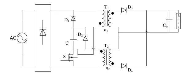
The SSBBDET converter (Fig. 2.1) consists of a diode bridge rectifier, a power switch S, transformers T1 and T2, a DC bus capacitor C, an output capacitor Co, and rectifier diodes D1 to D4. T1 and T2 have turns ratios of n1 and n2 and magnetizing inductances of Lm1 and Lm2,
16
The input current is discontinuous and is bounded by a sinusoidal envelope so that it is
essentially a sinusoidal waveform with high frequency harmonic components. The magnetizing
current of each transformer can be either discontinuous or continuous. To simplify the design, it
is assumed that these currents are discontinuous so that both transformers are fully demagnetized
by the end of the switching cycle.
The converter has two modes of operation, depending on the DC bus voltage VC. In the first
mode, transformer T1 acts like an inductor (i.e. it stores an amount of energy during an interval
and transfers this energy into another primary-side component on the next interval) while T2 acts
as a flyback transformer (i.e. it stores energy during an interval and transfers the stored energy to
the secondary-side on the next interval). In the second mode, both transformers act like flyback
transformers. Both modes are described in this section as following.
A. Mode 1: Single Flyback Transformer Mode of Operation
The converter operates in this mode when DC bus voltage VC is less than n1Vo, which is the
reflected output voltage on the primary side of transformer T1. As a result, diode D3 does not
conduct and no energy is transferred to the output through transformer T1; therefore, T1 becomes
like an input inductor. In this mode, T2 is the only transformer that actually operates as a flyback
transformer. When operating in this single flyback transformer mode, the converter operates in
the following two intervals. Typical converter waveforms and equivalent circuit diagrams are
shown in Figs. 2.2 and 2.3:
Interval 1 [t0–t1] (Fig. 2.3(a)): At the beginning of this interval, power switch S is turned on. As
a result, the rectified input line voltage |Vin| is applied to the magnetizing inductance of
AC
L o a d D1
D2
D3
D4
Co
C
T1
T2
S
n1
n2
17
transformer T1, Lm1. Current through Lm1, iLm1, begins to flow and increase linearly. Also during
this interval, DC bus voltage VCis applied across the magnetizing inductance of T2, Lm2, through D2, causing its current iLm2 to increase linearly. During this interval, there is no power transfer to
the load and it is just supplied by Co.
Interval 2 [t1 –t2] (Fig. 2.3(b)): Switch S is turned off at the beginning of this interval. As a
result, all the energy that was placed in T1 during Interval 1 is transferred to bus capacitor C, and
all the energy that was placed in T2 during Interval 1 is transferred to the output through D4. At
some instant t = t2, both T1 and T2 become fully demagnetized and remain in this condition until
the beginning of the next switching cycle.
B. Mode 2: Dual Flyback Transformer Mode of Operation
The converter enters this mode of operation when the DC bus voltage reaches n1Vo. Ideally, VC
can never exceed n1Vo because otherwise, diode D3 starts to conduct and allow energy (which
normally is supposed to charge the DC bus capacitor) to be transferred to the output. During this
18
secondaries when switch S is off. Part of the stored energy in the magnetizing inductance of T1
goes to the DC bus capacitor after S has been turned off. When operating in the dual flyback transformer mode, the converter operates in the following three intervals with typical converter
waveforms and equivalent circuit diagrams shown in Figs. 2.4 and 2.5, respectively.
Interval 1 [t0– t1] (Fig. 2.5(a)): The converter operates in the same way as the first interval of
Mode 1 and transformers T1 and T2 are charged linearly.
Interval 2 [t1 –t2] (Fig. 2.5(b)): Switch S turns off at t1 at the beginning of this interval. The
converter operates in the same way as in the second interval of Mode 1 and the energy stored in
T1 is transferred to C. Also during this time interval, all the energy that was placed in T2 in
interval 1 is transferred to the output through D4. The DC bus voltage reaches n1Voat t = t2 while T2 is not yet fully demagnetized.
Interval 3 [t2 –t3] (Fig. 2.5(c)): At t = t2, VC is equal to n1Vo and D3 begins to conduct as it
19
during this time interval, just as in interval 2, the rest of the energy that was placed in T2 in
interval 1 is transferred to the output through D4. At different instants in this interval, T1 and T2
become fully demagnetized and remain in this condition until the start of the next switching
cycle.
The advantages of the converter over conventional single-stage PFC converters are as follows:
1) The voltage stress on the main switch in this single-stage PFC converter is significantly
lower than conventional ones. Regardless of operation mode, the maximum voltage that
is placed across switch S occurs while T2 is demagnetizing and is
(2.1)
2) There are two mechanisms that make the DC bus voltage less variable in this converter
compared to previous single-stage PFC AC/DC converters. One is substitution of the
input inductor with a flyback transformer, which helps clamp the DC bus voltage. The
second is that the input section is based on a buck–boost converter instead of boost
converter. In this case, the variation in the DC bus voltage can be reduced so that when
the input line voltage is low, the buck-boost input section produces a DC bus voltage that
is higher than the peak input voltage, and when the input line voltage is high, the DC bus
voltage is lower than the peak of the input voltage. This is due to the nature of buck-boost
topology (which can step-up and step-down voltage) as low input line operation requires
larger duty-cycles, which makes the input section act as a boost converter. On the other
hand, high line operation requires smaller duty-cycles, which makes the input section
operate as a buck converter.The combination of these two mechanisms reduces potential
voltage variation.
2.3.
Steady-State Analysis and Converter Design
There are four key parameters that should be determined for the converter: the magnetizing
inductances for transformers T1 and T2, Lm1 and Lm2, and their turns ratios, n1 and n2. In this
section, these four parameters are determined as well as the voltage conversion ratio of the
converter (i.e. output DC voltage to input AC voltage). This can be achieved by performing a
steady-state analysis of the converter then using the results of the analysis to develop a procedure
20
analysis has already been performed in [39], the analysis and design procedure is replicated from
that work.
To simplify the analysis presented in [39], the following assumptions were made:
1) The converter is lossless.
2) The duty ratio of the converter is kept constant throughout the entire line cycle.
3) The switching frequency is much higher than the line frequency.
4) The leakage inductances of transformers are negligible.
5) Despite of slight changes in DC bus voltage, it is considered to be constant during each
line cycle.
To derive the voltage conversion ratio of the converter, the balance between the input power and
the output power should be considered. The converter peak input current Iin(t) can be
approximately expressed by the following equation, which is an equation of the voltage across
the magnetizing inductance of transformer T1, Lm1:
(2.2)
where is the peak value of the input voltage, is the line frequency, D is the duty ratio of the converter and is the switching time period. Since the switching frequency is much higher
than the line frequency, the input voltage can be considered constant at each switching cycle.
( means the voltage in kth switching cycle). As a result, the average input current in kth switching cycle, , can be derived as follows:
∫
(2.3)
The average power during kth switching cycle can be determined to be
(2.4)
and the average input power during half line cycle can be defined to be
∫
21
where is the line time period and is the switching frequency.
With T2 being fully demagnetized at the end of each line cycle, the average output power during
a half line cycle can be determined based on the voltage across its magnetizing inductance. Since
the DC bus voltage is constant during each line cycle, the following equations can be derived:
(2.6)
=
∫
(2.7)
(2.8)
Considering the power balance in the circuit (i.e. ), the following relation between
the DC bus voltage, , and the peak input voltage, can be obtained based on (2.5) and (2.8):
√ √
√ (2.9)
The standard voltage transfer ratio equation of a flyback converter (if assuming that T2 is
working in boundary level of being fully demagnetized and not) can be applied to find the
relationship between the DC bus voltage and output voltage as follows:
(2.10)
where n2 is the turns ratio of the transformer T2. Using equations (2.9) and (2.10), the desired
voltage conversion ratio of the converter can be determined to be
√
√ (2.11)
To find the key converter parameters (Lm1, Lm2, n1, n2), the following considerations should be
taken into account:
1) The converter should operate with a completely discontinuous input current bounded by a
sinusoidal envelope.
22
The above parameters will be designed for a converter with the following characteristics:
Input voltage: Vin = 85~265 Vrms
Output voltage: Vo = 48 Vdc
Maximum output power: Po = 100 W
Switching frequency: fsw = 100 kHz
A: Selection of magnetizing inductance of transformer T1, Lm1
Lm1 should be sufficiently low so that the magnetizing current of T1 does not become continuous,
which leads to Discontinuous Conduction Mode (DCM) operation of the converter. According to
eq. (2.5), the maximum value for Lm1 can be determined as
(2.12)
where is the maximum duty ratio (i.e. 0.5) corresponding to minimum AC input voltage,
. Substituting the parameter values into eq. (2.12) gives
( √ ) (2.13)
Lm1 = is selected for the prototype converter that is used in simulations and experimental
works.
B: Selection of turns ratio of transformer T1, n1
Turns ratio of transformer T1, n1determines the voltage level when the converter enters Mode 2,
the dual flyback transformer mode, as stated in Section 2.2. It also defines the maximum voltage
stress across the main switch as expressed in eq. (2.1). As a result
(2.14)
which results in
23
If the maximum voltage stress on the main switch is considered 500 V, maximum turns ratio of
transformer T1 can be found by substituting appropriate parameter values in eq. (2.15), which
gives the following equation:
√ (2.16)
n1 = 2.5 is chosen for the transformer T1 of the prototype converter incorporated in computer
simulations and experimental works.
C: Selection of magnetizing inductance of transformer T2, Lm2
Lm2 needs to be sufficiently high in order to transfer an appropriate amount of energy directly to
the output. Low magnetizing inductance of transformer T2 leads to more direct energy transfer
intervals in the converter’s operation; more direct energy transfer from transformer T1 means
more low frequency ripple on the output voltage, which is not desirable. Considering eq. (2.9),
the minimum value of Lm2 should be
(
) (2.17)
Substituting the parameter values into eq. (2.17) gives the minimum value for Lm2
(
√ ) (2.18)
Lm2 = is selected for the prototype converter.
D: Selection of turns ratio of transformer T2, n2
The value of n2 should be low enough to guarantee that the transformer T2 is fully demagnetized
at the end of each line cycle. The turns ratio of transformer T2 can be selected using the voltage
conversion ratio of the converter as in eq. (2.11). To determine the lowest possible value for n2,
low line converter operation should be considered, which means the input voltage is 85 Vrms.
Substituting the parameter values into eq. (2.11) gives
24
2.4.
Conclusion
In this chapter, the single-stage PFC AC/DC converter that is being considered in this thesis, the
SSBBDET converter, was discussed. The main advantage of this converter is that its DC bus
voltage variation is significantly less than that of other single-stage PFC converters, which
allows smaller size components specially DC bus capacitor to be used. This is the result of buck–
boost type input section and clamping of VC to n1Vo by the secondary winding of T1. In this
chapter, the operation of the converter and its various modes of operation were explained in
detail and key component values were selected by a design procedure. These component values
were used in a prototype converter from which experimental results were obtained, as will be
25
Chapter 3
Averaged State-Space Modeling and Small-Signal Analysis of the Single-Stage
PFC Converter
3.1.
Introduction
A small-signal state-space model of the Single-Stage Buck-Boost Direct Energy Transfer
(SSBBDET) converter is determined in this chapter to be used for designing the voltage and
current compensators of the proposed control scheme. In this chapter, the general approach for
modeling PWM converters with one inductor operating in Discontinuous Conduction Mode
(DCM) is explained and is used to develop a new method of performing averaged state-space
modeling for a PWM converter with multiple inductors operating in DCM, such as single-stage
PFC converters. The main idea behind this new approach is that the averaged state-space model
of a PWM converter with multiple inductors can be derived by first considering each inductor
separately using the general averaged state-space model for PWM converters with one inductor,
then adding all these separate models to obtain the model for the whole converter. It is shown
how a small-signal model and key transfer functions can be extracted from the average
state-space model of such a converter. The output to input small-signal transfer functions of the
SSBBDET converter are used to keep the small-signal values at zero so that the states of the
26
3.2.
Averaged State-Space Modeling of PWM Converters with One Inductor
Operating in DCM
Several approaches have been proposed to model the dynamic behaviour of PWM converters
operating in discontinuous conduction mode (DCM) [63]-[67], with the most popular approach
being averaged state-space modeling. The general form of an averaged state-space model is
̇ (3.1)
where x is a vector representing the states of the system, u is the vector of the control inputs of
the system, and A and B are numerical matrices that are dependent on the parameter values of
the converter. In the averaged state-space modeling approach for PWM converters, the averaged
current of each inductor and the averaged voltage of each capacitor are considered as the states
of the system over a switching cycle. The model is then determined using KCL (Kirchhoff’s Current Law) and KVL (Kirchhoff’s Voltage Law) equations for the inductors and capacitors.
The input inductor of a low power PWM boost converter like the one shown in Fig. 3.1 generally
operates in DCM. In order to develop an averaged state-space model for a DCM PWM converter
with one inductor such as the boost converter shown in Fig. 3.1, three time-intervals can be
considered for each switching cycle, as indicated by , and in Fig. 3.2. A
piecewise-linear state-space model can be written for each time-interval in a switching cycle as
follows:
̇ for (3.2) ̇ for (3.3)
̇ for (3.4)
where is the only input of the DCM operating PWM converter and is the time period of
DC
Input Inductor
27
Fig. 3.2 Time intervals of inductor current in a DCM operating converter.
i
LiLpk
Ts
d1Ts d2Ts d3Ts
each switching cycle. An averaged state-space model can be applied to equations (3.2) - (3.4) to
obtain the averaged model of the converter operating in DCM as
̇ [ ] [ ] (3.5)
where denotes the average value of the states of the system over a switching cycle. Equation
(3.5) is the general form of averaged state-space model of a PWM converter operating in DCM,
but the average value for inductor current determined by eq. (3.5) is not necessarily the true
average value of the state variable. The average value of the inductor current based on the
state-space model, expressed by eq. (3.5) can be compared with the average obtained from the actual
value of the charge in the capacitor to determine that eq. (3.5) does not result in a true average
value. This can be shown as follows:
Based on the waveform in Fig. 3.2, the average of the input inductor current operating in
discontinuous mode over a switching cycle can be written as
(3.6)
where is the peak value of inductor current in a switching cycle. Full details on how eq.
(3.6) is derived from Fig. 3.1 can be found in Appendix A.
Consider the case in which a capacitor is connected to the input inductor when the switch is on.
The averaged state-space model in eq. (3.5) implies that the charging current of the capacitor
28
(3.7)
On the other hand, to obtain the average value of the charging current over the capacitor using
KCL expressions, the average charge that the capacitor receives from the inductor in a switching
cycle is
∫ (3.8)
which determines the actual average charging current of
(3.9)
The actual average charging current in eq. (3.9) obtained from the KCL equations is different
from the value in eq. (3.7) obtained from averaged state-space model. This implies that the
averaged state-space model of eq. (3.5) is somehow deficient in representing the actual
behaviour of the PWM converter.
One approach to improving the accuracy of the model is to divide the inductor currents in eq.
(3.5) by as this term is the difference between the actual average value and the
average value in the state-space model. In order to divide the inductor currents by the
state vector should be rearranged as [ ] where vectors and contain the inductor
current and all the capacitor voltages, respectively. The averaged state-space model in eq. (3.5)
can then be rewritten as
̇ [ ] [ ] (3.10)
in which M is
[ ⏟
⏟
] (3.11)
29
For the model represented in eq. (3.10) some modifications still need to be made so the model
can be used to design the control system of PWM converters with a single inductor that operates
in DCM. For such a converter, the only control variable that is used for output voltage regulation
is the duty-ratio . This means that should be replaced by an expression of in the averaged
state-space model of the converter; the peak value of the inductor current can be used to
determine such an expression.
In general, if the voltage across each inductor in a PWM converter is when the switch is
turned on, then using the inductor current equations for the first time-interval (inductors
generally store energy during the first time-interval in PWM converters), the peak value of the
inductor current can be expressed as
(3.12)
Substituting this into eq. (3.6) results in
(3.13)
in which is an expression of and can be replaced in eq. (3.10). Substituting (3.13) into
(3.10) results in the general averaged state-space model of a converter with one inductor
operating in DCM as follows:
̇ [ (
) ( (
)) ] [ (
)
( (
)) ] (3.13A)
3.3.
Averaged State-Space Modeling of the Single-Stage PFC AC/DC
Converter with Direct Energy Transfer
Previously proposed averaged state-space models for PWM converters with multiple inductors
can be generally categorized into two major classes:
30
2) Full-order averaged models in which all inductor currents and capacitor voltages are retained in the model.
The major drawback of the reduced-order approach when used in the modeling of single-stage
PFC AC/DC converters (in which two inductors are used, the input inductor and the magnetizing
inductance of the transformer) is the elimination of the input inductor current, which is the main
variable to be considered in input current shaping. Full-order models are therefore more accurate
than reduced-order models for modeling single-stage PFC converters. A full-order model is
developed in this thesis work to model the behaviour of the SSBBDET converter.
The magnetizing inductances of the two transformers (T1 and T2) of the SSBBDET converter can
be considered as the inductors of the converter and their currents ( , ) waveforms are
shown in Fig. 3.3. It can be seen from this figure that four time-intervals (
) occur during a switching cycle. The modified averaged state-space model in eq. (3.10) that is
generally used to model PWM converters with one inductor in their topology cannot be used in
the modeling of the SSBBDET converter. The SSBBDET converter has four time-intervals in a
switching cycle (Fig. 3.3), but only three time-intervals are considered in the modified averaged
state-space model in eq. (3.10). As a result, a new scheme for modeling the SSBBDET converter
is proposed in this section; this scheme is basically a modification of the modified averaged
state-space model in eq. (3.10). The main idea behind this new scheme is that the modified
averaged state-space model in eq. (3.10) is derived for each inductor in the converter and all
iLm1
iLm1pk
Ts
d1Ts d2Ts d3Ts iLm1pk
iLm2
d4Ts
t1 t2 t3
31
these derived models are merged together to obtain the averaged state-space model for the
SSBBDET converter with multiple inductors that are all operating in DCM.
The currents of the magnetizing inductances ( , ) of the transformers (i.e. that are
assumed as the inductors of the converter) and the voltages of the capacitors ( are
considered as the states of the converter to be used in the averaged state-space model. According
to the operation modes of the converter discussed in Section 2.2, the state equations of the
converter for each time-interval can be written as follows:
A: Switch is ON, 0 < t < t1
(3.14)
(3.15)
(3.16)
B: Switch is OFF, t1 < t < t2
(3.17)
(3.18)
(3.19)
C: Switch is OFF, t2 < t < t3
(3.20)
(3.21)
(3.22)
D: Switch is OFF, t3 < t < t4
(3.23)
In order to use the modified averaged state-space model in eq. (3.13A) for each inductor, matrix
M should be defined. As the average values in equations (3.7) and (3.9) were obtained based on
32
any inductor operating in DCM in a PWM converter with multiple inductors such as the
SSBBDET converter. As a result matrix M can be rewritten for the SSBBDET converter as
follows:
[ ⏟
⏟
] (3.24)
which results in:
[
] (3.24A)
By substituting equations (3.14) – (3-23) and eq. (3.24A) into eq. (3.10), the averaged state-space
equations for each state inductor and state capacitor can be written as follows:
(3.25)
(3.26)
(3.27)
In order to define the modified averaged state-space model in eq. (3.13A), and should be
defined as an expression of as it is the only control variable that is used for output voltage
regulation. In order to obtain the average values of the inductor currents based on eq. (3.6), the
peak values of and must be determined first; these can be written using eq. (3.12) as
follows:
(3.28)
(3.29)
and using eq. (3.6) for the average values of the inductor currents results in
![Fig. 1.7 Peak current control scheme on a boost PFC converter [42].](https://thumb-us.123doks.com/thumbv2/123dok_us/7785830.1287982/22.612.203.406.529.691/fig-peak-current-control-scheme-boost-pfc-converter.webp)
![Fig. 1.8 Hysteresis current control on a boost PFC converter [42].](https://thumb-us.123doks.com/thumbv2/123dok_us/7785830.1287982/23.612.213.398.537.690/fig-hysteresis-current-control-boost-pfc-converter.webp)
![Fig. 1.9 Average current mode control on a boost PFC converter [42].](https://thumb-us.123doks.com/thumbv2/123dok_us/7785830.1287982/25.612.194.419.500.680/fig-average-current-mode-control-boost-pfc-converter.webp)