c e-ISSN: 2348-6848, p- ISSN: 2348-795X Volume 3, Issue 01, January 2016
International Journal of Research (IJR)
Available at http://internationaljournalofresearch.org
PV Cell based Single Stage Step-Up/Step-Down DC–AC
Converter
I.Denash Kumar
1& K.Kranthi Pratap Singh
21
M.Tech Scholar,Dept. of EEE, ASR College of Engineering and Technology, JNTUK, A.P
2
Assistant Professor, Dept. of EEE, ASR College of Engineering and Technology, JNTUK, A.P
Abstract: —
Single stage Buck/Boost inverter is an converter which performs two actions in a single stage. It boosts the DC voltage and invert to AC in a single stage. In Conventional two stage converter there will be two stages. The first stage will be a boost or buck boost DC-AC converter which is meant for
conditioning and leveling the DC voltage
approximately to invert to AC voltage required. The second stage will be an inverter, to invert the DC output obtained from first stage to AC voltage. This paper presents a new step-up/step-down DC-AC converter which is having application where an instantaneous voltage higher or lower than input DC voltage is required. It consists of one switching cell including two switches, two diodes, one inductor, and one capacitor on each inverter leg. . Validating the theoretical analysis, a prototype was designed, built, and tested for an output rated power of 1 kW, a dc input voltage of 96Vdc , and output voltage of 110 V rms. Furthermore, the fundamental output frequency was established at 60 Hz and the switching frequency at 20 kHz. Computer simulation by MATLAB/ SIMULINK has been used to support the developed concept.
Keywords: DC–AC converter; switching cell; Switched Capacitor circuit; Switched Capacitor
I.
I
NTRODUCTIONThe rate at which the demand of electrical energy increasing is high now. Conventional sources cannot meet these much demand. So there is a greater depend on non-conventional sources. When depending non- conventional sources, it leads to the development of efficient and low cost power conditioning units to serve as an interface between source and grid. So PCU forms an integral part in power conversion system. Depending on the voltage level, the PCU may be required to “buck” or “boost” the available dc voltage to meet the grid voltage requirements. Depending on the number of power
stages used, a PCU may be a single stage or multi stage configuration. For example, Using the buck inverter configuration, proposed by Yang and Sen. [5], power can be fed into the grid from a source whose voltage is greater than the peak grid voltage. Some other two-stage topologies have been proposed [6] which consist of a buck–boost converter cascaded in series with an H-bridge inverter operating at the grid frequency and providing sinusoidal power to the grid. Other two-stage topologies [7], [8] consist of a boost converter stage cascaded with an H-bridge inverter.
In spite of all the advantages offered by a two stage PCU, the presence of more number of power stages undermines the overall efficiency, reliability and compactness of the system besides increasing the cost. Therefore, today the trend is towards the integration of the various stages of a multistage PCU into a single-stage system with as many desirable features of multistage systems [9], [10] as possible. Though a single-stage PCU offers reduced control options (resulting in increased control complexity), these configurations have the advantages of low cost, high efficiency and reliability, modularity, and compactness.
c e-ISSN: 2348-6848, p- ISSN: 2348-795X Volume 3, Issue 01, January 2016
International Journal of Research (IJR)
Available at http://internationaljournalofresearch.org
Many single-stage buck–boost inverter configurations have also been proposed [10], [11], [12]. These configurations feed sinusoidal power into the grid with lower total harmonic distortion (THD) in the grid current and interface nicely with the grid. They also provide an inherent isolation between the source and the grid in the sense that there is an inductor that stores the energy from the source during switch-ON interval and delivers it to the grid during OFF interval without any direct connection between the source and the grid. However, the buck–boost inverter configurations suffer from high peak inductor current stress which is a result of the fact that the entire energy that is transferred to the grid in a switching cycle is stored in the inductor during the ON time of the switching cycle and only this stored energy is supplied to the grid during the OFF time of the switching cycle. This restricts its use to low power applications. Taking a cue from the above observations, this paper presents a new single-stage inverter topology. Due to the simple structure and low control complexity of the new converter, it is used in applications where an instantaneous voltage higher or lower than input DC is required.
II.
PROPOSED TOPOLOGY
–
SINGLE
STAGESTEP-UP/STEP-DOWN DC-AC
CONVERTER
A.
Basic diagram of the proposed converter :
The block diagram of the proposed
converter is shown in Fig.1. It consists of an
input DC voltage source which is fed to the
buck/boost converter .The gate signals for the
switches in the inverter is obtained through
Bipolar modulation is one of the technique
among sinusoidal pulse width modulation. In
bipolar modulation the pulses are obtained by
comparing a high frequency carrier signal with
a low frequency sinusoidal signal which is the
modulating or reference signal. Switching
signals are generated by comparing a high
frequency triangular waveform (Vp(t)) with
the control voltage Vcontrol (Vc(t)). The
control voltage is a modulating sine waveform.
Fig.1. Block diagram of the proposed converter
Fig. 2. Representative scheme of bipolar modulator
The output power stage of converter is shown in Fig.3. It consists of an input voltage source Vi, a loadresistance RR0R, two switching cells with elementsSR1R ,DR1R,CR1R,SR2R ,DR2R
andLR1R on one cell
andSR3R,DR3R,CR2R,SR4R,DR4 Rand LR2R on another cell and a high frequency filter with LRFR and CRFR.
Fig.3. Output power stage of converter
B. Modes of operations and design parameters:
c e-ISSN: 2348-6848, p- ISSN: 2348-795X Volume 3, Issue 01, January 2016
International Journal of Research (IJR)
Available at http://internationaljournalofresearch.org
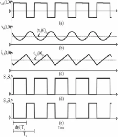
corresponds to the closing
of switches SR1R and SR4 Rand off stage corresponds to the opening of switches SR1R and SR4R. The switching pulses for SR1R and SR4R is same whereas for SR2R and SR3R is just the complementary of SR1R and SR4R
There are five operating modes in one switching period.
1. Mode 1: During on stage, when the switches SR1R and SR4R is closed at time t=0 the full input voltage appears across the inductor LR1R. After time t increases the current through inductor LR1R starts rising whereas the voltage across it starts decreasing. This voltage starts appearing across the another closed path where this voltage plus the gradually discharging voltage of capacitor makes the voltage at the output higher than that of input. The input current, which rises flows through capacitor CR1R, filter inductor LRfR, filter capacitor CRf, Rand load resistor RR0 . RAt the same time the capacitor CR2R discharges its voltage to the inductor LR2 Rso that the current through inductor LR2R starts increasing.
Fig.4. Mode -1 operation
2. During off stage, when the switches SR1R and SR4R is off the early charged inductor LR2 Rget discharged towards the source. The early charged inductor LR1R gets discharged through the capacitor CR1R thereby this capacitor CR1R gets charged. On comparing the waveform it is obtained that the equivalent circuits for the two cases are similar only the current direction through all the elements is reversed. Since the current direction reverses through all the elements in effect the two circuits are same
so for an extended analysis we are considering only the circuits for duty cycle higher than 0.5.
Fig.5. Mode -2 operation
Fig.6. Mode -3 operation
Fig.7. Mode -4 operation
c e-ISSN: 2348-6848, p- ISSN: 2348-795X Volume 3, Issue 01, January 2016
International Journal of Research (IJR)
Available at http://internationaljournalofresearch.org
CR1R, CR2 Rand the command signals applied to switches SR1R, SR4 Rare shown in Fig. 10
Fig. 8. Simulation waveforms: (a) voltage between terminals A and B; (b) voltage across capacitor CRfR ; (c)
current through inductor LRfR ; (d) command signal applied to switches SR1R and SR4R ; (e) command signal
applied to switches SR2R and SR3R .
Fig. 9. Simulation waveforms: (a) voltage across inductor LR1 R; (b) current through inductor LR1R ; (c)
voltage across inductor LR2R ; (d) current through
inductor LR2R ; (e) input current; (f) command signal applied to switches SR1 Rand SR4R .
Fig. 10. Simulation waveforms: (a) voltage across the capacitor CR1 R; (b) current through capacitor CR1R; (c)
voltage across the capacitor CR2R; (d) current through capacitor CR2R; (e) command signals applied to switches
SR1 Rand SR4R .
c e-ISSN: 2348-6848, p- ISSN: 2348-795X Volume 3, Issue 01, January 2016
International Journal of Research (IJR)
Available at http://internationaljournalofresearch.org
So from this duty cycle is obtained as a function of static gain. So the function given in the block F is
III. MATLAB BASED SIMULATION &RESULTS
In power stage four MOSFET switches are used. Proposed circuit is simulated with open loop control, in which, output voltage is controlled by varying amplitude of the reference sine wave, in effect duty cycle, D, corresponding to maximum value of output voltage. With Vo = 110VRrmsR,Vi = 96VRdcR, R = 12Ω, Fs = 20kHz as per design equations value of inductor is obtained as LR1R, LR2R = 255 μH and value of capacitors CR1R, CR2R is obtained as C = 1μF. Inorder to eliminate high switching frequency component from output voltage, cutoff frequency of output filter is
decided as
1800Hz. Then filter inductor is obtained as LRf R= 1.5 mH.Fig.6.1 shows output voltage is a pure sinusoidal waveform and the output voltage is about 110 Vrms. To verify the feasibility of the proposed system a simulink model is developed. Fig.11 shows the sub system in the simulink model.
All the mathematical calculated simulatution parameters are given by table.1
Fig.11.MATLAB based simulation diagram of proposed system with masked diagrams
Fig.12.MATLAB based simulation diagram of proposed system with masked blocks for output responses
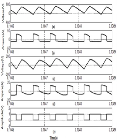
Fig.13.MATLAB based simulation diagram of proposed system –Output voltage and current waveform for R-load
Fig.14.MATLAB based simulation diagram of proposed system – (a) voltage between terminals A and B; (b)
c e-ISSN: 2348-6848, p- ISSN: 2348-795X Volume 3, Issue 01, January 2016
International Journal of Research (IJR)
Available at http://internationaljournalofresearch.org
SR1R and SR4R; (e) command signal applied to switches SR2 Rand SR3R.
Fig. 14 (a) shows that During mode 1 the voltage across the terminals A and B starts decreasing in the positive direction whereas during off time voltage starts increasing in negative direction. Fig. 14 (b) shows that the output voltage is a pure sinusoidal waveform. Fig. 14 (c) shows that the current across inductor is firstly increases and then decreases linearly. When a switch SR1 Rand SR4R is on, current increases and reaches a final value. When switches SR1R and SR4R is off current across inductor decreases from its final value. This is the case when duty cycle greater than 0.5. When duty cycle is below 0.5, current starts increasing in negative direction during switches SR1R and SR4R is on. When off current starts decreasing from the negative side. Fig. 14 (d) shows the pulses given to switch SR1R and SR4R. The compliment of above pulse is for switch SR2R and SR3R. For producing these pulses triangular wave compared with a duty ratio waveform and then given to relational operator. When the amplitude of duty ratio waveform is higher than that of triangular wave, pulses are generated.
Fig. 15. Simulation waveforms 3: (a) voltage across the capacitor CR1 R; (b) current through capacitor CR1 R;
(c) voltage across capacitor CR2 R; (d) current through capacitor CR2 R; (e) command signals applied to switches
SR1R and SR4R.
Fig.14 (a) shows that the voltage is positive during Switches SR1 Rand SR4 Ris on. At that time current is increasing and reaches final value. When switches SR1R and SR4R is off the voltage starts increasing in the negative direction where as current starts decreasing.
Fig.14 (c) shows that the voltage is negative and starts increasing during on time and positive remains constant during off time and the current is decreasing and then increasing and it is negative too. Fig.15 (a) shows that the voltage is positive during Switches SR1 Rand SR4 Ris on. At that time current is increasing and reaches final value. When switches SR1R and SR4R is off the voltage starts
increasing in the
negative direction where as current starts decreasing. Fig.15 (c) shows that the voltage is negative and starts increasing during on time and positive remains constant during off time and the current is decreasing and then increasing and it is negative too.
APPENDIX TABLE.I.SIMULATION SPECIFICATIONS
Parameter Rating
Input dc voltage 96 Vdc
Output dc voltage 110 V Maximum output
power
1 kW
Switching frequency 20 kHz output voltage
frequency
50Hz
CONCLUSION
This paper presented a new topology for dc–ac converters whose main feature is its capacity to provide an instantaneous output voltage higher or lower than the input voltage without an intermediate power stage or transformer. The circuit configuration of proposed converter is very simple and it is modified form of the Buck-Boost inverter. The advantages of the circuit are low cost, high efficiency, low component counts etc. Analysis and design of the overall system were discussed. In future the system can be made to closed loop by using any feedback controller. The closed loop control improves system dynamic response and it provides a good regulated output voltage. Based on theoretical analysis and simulation results the following conclusions can be drawn:
1) The evaluated performance was in agreement with
the theoretical analysis;
c e-ISSN: 2348-6848, p- ISSN: 2348-795X Volume 3, Issue 01, January 2016
International Journal of Research (IJR)
Available at http://internationaljournalofresearch.org
operations .
3) It can be used in applications where instantaneous voltage higher or lower than DC voltage is required
R
EFERENCES[1]
M. Jang and V. G. Agelidis, “A minimum
power-processing-stage fuelcell energy system
based on a boost-inverter with a bidirectional
backup battery storage,”
IEEE Trans. Power
Electron.
,
vol.
26,
no.
5,
pp.
1568–
1577, May 2011.
[2]
K. Beer and B. Piepenbreier, “Properties
and advantages of the quasi-Zsource inverter for
DC–AC
conversion
for
electric
vehicle
applications,”
Proc.
Electr.
Power
Train
Emobility
, pp. 1–6, 2010.
[3]
A.
Florescu,
O.
Stocklosa,
M.
Teodorescu, C. Radoi, D. A. Stoichescu, and S.
Rosu, “The advantages, limitations and
disadvantages of Z-source inverter,” in
Proc.
2010 Int. Semicond. Conf. (CAS)
, Oct. 2010, vol.
2, pp. 483, 486.
[4]
B. S. Prasad, S. Jain, and V. Agarwal,
“Universal single-stage gridconnected inverter,”
IEEE Trans. Energy. Convers.,
, vol. 23, no. 1,
pp. 128– 137, Mar. 2008.
[5]
T.F. Wu, Y.S. Lai, J.C. Hung and Y.M.
Chen, ―Boost Converter with Coupled
Inductors and Buck–Boost Type of Active
Clamp‖
IEEE Trans Ind. Electron.,
vol. 55, no. 1,
Jan. 2008.
[6]
B.
Axelrod,
Y.
Berkovich
and
A.Ioinovici, ―Switched
Capacitor/Switched-Inductor Structures for Getting Transformerless
Hybrid DC–DC PWM Converters‖,
IEEE Trans
Circuits And Systems—I: Regular Papers,
Vol.
55, no. 2, Mar 2008.
[7]
D. Sabin and A. Sundaram, "Quality
enhances
reliability,"
IEEE Spectrum
, vol. 33, no. 2,
Feb. 1996, pp. 34-41.
[8]
R.J. Wai, C.Y. Lin, C.Y. Lin, R.Y. Duan
and Y.R. Chang, ―HighEfficiency Power
Conversion
System
for
Kilowatt-Level
StandAlone Generation Unit with Low Input
Voltage‖,
IEEE Trans Ind.Electron.,
vol. 55, no.
10, Oct 2008.
[9]
G.S. Yang, T.J. Liang and J.F. Chen,
―Transformerless DC–DC Converters With
High
Step-Up
Voltage‖,
IEEE
Trans
Ind.Electron.,
vol. 56, no. 8, Aug 2009.
[10]
J.M. Burkhart, R. Korsunsky, and D.J.
Perreault, ―Design Methodology For A Very
High Frequency Resonant Boost Converter‖,
IEEE Trans. Power Electron.,
vol. 28, no. 4, Apr
2013.
[11]
F.S. Garcia, J.A. Pomilio and G. Spiazzi,
―Modeling and Control Design of the
Interleaved Double Dual Boost Converter‖,
IEEETrans Ind. Electron.,
vol. 60, no. 8, Aug
2013.
[12]
F.H. Dupont, C. Rech, R. Gules and J. R.
Pinheiro, ―Reduced Order Model and Control
Approach for the Boost Converter With a
Voltage Multiplier Cell‖,
IEEETrans Power
Electron.,vol
.
28, no. 7, July 2013.
[13]
R. J. Wai and R. Y. Duan, ―High
step-up converter with costep-upledinductor,‖
IEEE
Trans.Power Electron.,
vol. 20, no. 5, pp. 1025–
1035, Sep. 2005.
[14]
R. J. Wai, L. W. Liu and R. Y. Duan,
―High efficiency voltage clamped dc–dc
converter with reduced reverse-recovery current
and switch voltage stress,‖
IEEE Trans. Ind.
Electron..,
vol. 53, no. 1, pp. 272–280,Feb. 2005.
[15]J. W. Baek, M. H. Ryoo, T. J. Kim, D. W.
Yoo and J. S. Kim, ―High boost converter using
voltage multiplier,‖ in
Proc. IEEEIECON
, 2005,
pp. 567–572.
[16]