c e-ISSN: 2348-6848, p- ISSN: 2348-795X Volume 2, Issue 12, December 2015
International Journal of Research (IJR)
Available at http://internationaljournalofresearch.org
Input side PFC and Output side Voltage variation with Closed loop
AC-DC Converter
Md Hakeem Baba
M-tech Student Scholar Department of Electrical & Electronics Engineering, VIF College of Engineering
and Technology, Himiyatnagar, RangaReddy, TS, India
D. Subhani
M.Tech
Assistant Professor Department of Electrical & Electronics Engineering, VIF College of Engineering
and Technology, Himiyatnagar, RangaReddy, TS, India
Abstract-
In this paper closed loop control of a
three-level integrated ac–dc converter is proposed.
The proposed converter integrates the operation of
the boost power factor correction and the
three-level ac–dc converter. By the implementation of
PI controller with PWM technique in closed
loop, the switching sequence is under controlled
condition and the output voltage of the proposed
converter effectively increases. To improve the
performance of the ac–dc converter, two bulk
storage capacitors are adopted. Its excellent line
regulation capability makes the converter suitable
for universal input application. The converter is
made to operate with two independent controllers
an input controller that performs power factor
correction and regulates the dc bus and an output
controller that regulates the output voltage. They
consist of an ac–dc boost pre regulator converter
that shapes the input current and an isolated dc–dc
full-bridge converter that converts the pre
regulator output into the required dc voltage.
They
use passive elements such as inductors and
capacitors to filter low frequency input current
harmonics and make the input current more
sinusoidal. Two stage converters, however, require
two separate switch-mode converters (each with its
own controller), and thus, can be expensive.
Moreover, they have poor efficiency when
operating under light-load conditions as there are
two converter stages that are operating each with
its own set of fixed losses while a small amount of
power is actually transferred to the load. The
simulations
results
are
conferred
using
Matlab/Simulink platform.
Index Terms—
AC–DC power conversion;
single-stage power factor correction (SSPFC); three-level
converters.
I. INTRODUCTION
c e-ISSN: 2348-6848, p- ISSN: 2348-795X Volume 2, Issue 12, December 2015
International Journal of Research (IJR)
Available at http://internationaljournalofresearch.org
factor correction can be classified into two stage
scheme. Two stages PFC contain two independent
power stages in cascade with PFC stage and
DC-DC regulator. The total efficiency of the two stages
is lower because the total power has to be
processed twice with two cascade power stage.
Cost of the circuit is increase several schemes have
developed to combine stage into one stage.
The open loop control of a three level
integrated ac-dc has very less output voltage.
To
regulate the excessive dc bus voltages, minimize
the large output ripples, distorted input currents
and for better output voltage there is a need for a
converter, which overcomes all these drawbacks.
In this paper, a closed loop control of a single
stage three level integrated ac–dc converter that
does not have the drawbacks of previously
proposed single-stage and two-stage converters
is proposed.
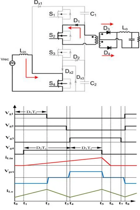
Fig.1.Single-stage three-level AC-DC converter in open loop condition
II. OPERATION OF THE PROPOSED CONVERTER
The operation of proposed converter in open loop condition, which is shown in Fig. 1, integrates an ac–dc boost PFC converter into a three-level dc–dc converter. The ac–dc boost section consists of an input diode bridge, boost Inductor Lin,
boost diode Dx1, and switch S4, which is shared by the
multilevel dc–dc section. When S4is off, it means that no
more energy can be captured by the boost inductor. In this case, diode Dx2 prevents input current from flowing to the
midpoint of capacitors C1 and C2 and diode Dx1 conducts and
helps to transfer the energy stored in the boost inductor Lin to
the dc bus capacitor. Diode Dx3 bypasses Dx2 and makes a
path for circulating current. Although there is only a single converter, it is operated with two independent controllers. One controller is used to perform PFC and regulate the
voltage across the primary side dc-bus capacitors by sending appropriate gating signals to S4. The other controller is used
to regulate the output voltage by sending appropriate gating signals to S1to S4.It should be noted that the control of the
input section is decoupled from the control of the dc–dc section and thus can be designed separately. The gating signal of S1, however, is dependent on that of S4, which is the output
of the input controller; how this signal is generated is discussed in detail later in this paper. The gating signals for S2
and S3 are easier to generate as both switches are each ON for
half a switching cycle, but are never ON at the same time. Typical converter waveforms are shown in Fig. 2 and equivalent circuit diagrams that show the converter’s modes of operation are shown in Fig. 3 with the diode rectifier bridge output replaced by a rectified sinusoidal source. As the input line frequency is much lower than the switching frequency, it is assumed that the supply voltage is constant within a switching cycle. It is also assumed that the input current is discontinuous, although there is no reason why the input current cannot be made to be continuous if this is what is desired. The converter has the following modes of operation:
1) Mode 1 (t0 ≤t≤t1): During this mode, switches S1and S2 are
ON and energy from dc-bus capacitorC1 is transferred to the
output load. In the output section, a positive voltage of (Vpri/n) VO (where n is the ratio of primary to secondary
transformer turns) is impressed across Lo and the current through it rises.
2) Mode 2 (t1 ≤t≤t2): In this mode, S1 andS2 remain ON andS3
turns ON. The energy from dc bus capacitor C1 is transferred
to the output load. At the same time, the diode bridge output voltage Vrec is impressed across input inductor Lin so that the
current flowing through this inductor rises.
3) Mode3 (t2 ≤t≤t3): In this mode, S1 andS2 remain ON andS3
turns ON. The energy from dc bus capacitor C1is transferred
c e-ISSN: 2348-6848, p- ISSN: 2348-795X Volume 2, Issue 12, December 2015
International Journal of Research (IJR)
Available at http://internationaljournalofresearch.org
voltage Vrec is impressed across input inductor Lin so that the
current flowing through this inductor raises voltage Vrec is
impressed across input inductor Lin so that the current flowing through this inductor rises.
Fig. 2. Typical waveforms describing the modes of operation.
4) Mode 4 (t3 ≤t≤t4): In this mode, S1 andS2 are OFF and S4 is
ON. The current in the primary of the transformer charges capacitorC2 through the body diode of S3 and
Dx3.
5) Mode 5 (t4 ≤t≤t5): In this mode, S3 andS4 are ON. Energy
flows from capacitorC2flows into the load while the current
flowing through input inductor Lin continues to rise.
6) Mode 6 (t5 ≤t≤t6): In this mode, S4 turns off. The current in
input inductor flows thorough the diodeDx1 to charge the
capacitors C1 andC2. The current in the transformer primary
flows thorough the S3 andD2.This mode ends when the
inductor current reaches zero. Also during this mode, the load inductor current freewheels in the secondary of the transformer.
7) Mode 7 (t6 ≤t≤t7): In this mode, the load inductor current freewheels in the secondary of the transformer. This mode ends when the switches S3turns off.
8) Mode 8 (t7 ≤t≤t8): In this mode, S3 is OFF and the current
in the primary of the transformer charges capacitor C1 through
the body diodes of S1 andS2. Finally, converter reenters
c e-ISSN: 2348-6848, p- ISSN: 2348-795X Volume 2, Issue 12, December 2015
International Journal of Research (IJR)
Available at http://internationaljournalofresearch.org
III. CONTROL STRATEGY
This section mainly focused on the control technique for the Single stage three level controllers. Closed loop PI controller with PWM technique gives the better performance as compared with the conventional converter. The block diagram of the proposed control technique is shown in Fig 3.
PI controller receives output voltage as input signal. Based on the input signal the PI controller generates a reference dc voltage signal which is an input signal to PWM generator. The values of PI controller gains (i.e Integral gain and proportional gain) are tuned in order to attain better output voltage. The PWM generator compares the dc reference signal with the saw tooth carrier signal and generates the pulses.
COVERTER CIRCUIT PI controller Pulse generation Vref Vact -+ SUPPLY LOAD
Fig.3. Block diagram of proposed system
IV.CONVERTER FEATURES
The proposed converter has the following features:
A. Reduced cost compared to two-stage converters: Although
the proposed converter may seem expensive, the reality is that it can be cheaper than a conventional two-stage converter. This is because replacing a switch and its associated gate drive circuitry with four diodes reduces cost considerably even though the component count seems to be increased—this is especially true if the diodes are ordered in bulk numbers.
B. Better performance than a single-stage converter:
The proposed single-stage converter can operate with a better input power factor for universal input line applications than a single-controller, single-stage because it does have a
dedicated controller for its input section that can perform PFC and regulate the dc-bus voltage. The presence of a second controller also allows the converter to operate with better efficiency and with less output ripple as each section.
C. Improved Light-Load Efficiency:
The proposed converter can be designed so that it has a conventional dc-bus voltage of 400 V. Since the converter is a multilevel converter, a 400 V dc bus means that each switch will be exposed to a maximum voltage of 200 V. Having 200 V across a MOSFET device instead of 400 V (as is the case with two-level converters) results in a 75% reduction in turn on losses when the converter is operating under light-load conditions and there is an insufficient amount to current available to discharge the switch output capacitances before the switches are turned on.
D. Increased Design Flexibility:
Since the converter is a multilevel converter, it can be operated with high dc-bus voltage (800 V), standard dc-bus voltage (400 V), or any dc-bus voltage 400 V<Vbus<800 V. There are advantages to operating with high dc-bus voltage or with standard dc bus voltage. The fact there is flexibility in the level that the dc-bus voltage is set means that there is considerable flexibility in the design of the converter. This gives the designer options as to how to optimize the design of the converter for other factors such as efficiency profile and cost (i.e. cost of switches based on voltage rating considerations and availability). It should be noted that this design flexibility makes the design of the three-level converter to be much simpler than that of a single-stage two-level converter or that of a single-controller three-two-level single stage converter as the dc-bus voltage can be fixed to a desired level that is considered appropriate. It should be noted that although the proposed converter has the aforementioned advantages over the conventional two-stage converter, it will have lower heavy-load efficiency because of increased conduction losses as switch S4 must conduct both the input current and the full-bridge current. As a result, when determining whether to use the proposed converter versus a conventional two-stage converter, the main trade off that needs to be considered is lower cost and improved light-load efficiency versus heavy-load efficiency.
V. MATLAB/SIMULINK RESULTS
c e-ISSN: 2348-6848, p- ISSN: 2348-795X Volume 2, Issue 12, December 2015
International Journal of Research (IJR)
Available at http://internationaljournalofresearch.org
Fig.4:Matlab/Simulink circuit of Single-Stage Three-Level Converter in open loop condition.
Fig.5: Input Current and Voltage Wave Forms
Fig.6: Voltage across Switch S1
Fig.7: Voltage across Switch S2
Fig.8: Voltage across Switch S3
Fig.9: Voltage across Switch S4
Fig.10: Three Level Output Voltage at primery side of transformer
c e-ISSN: 2348-6848, p- ISSN: 2348-795X Volume 2, Issue 12, December 2015
International Journal of Research (IJR)
Available at http://internationaljournalofresearch.org
Fig.12. FFT window for input current
Case ii: Single-Stage Three-Level Converter Under closed loop condition
Fig.13:Matlab/Simulink circuit of Single-Stage Three-Level Converter in closed loop condition.
Fig.14: Output Voltage
Fig.15. FFT window for input current
VI.CONCLUSION
A closed loop control of a three level
integrated ac–dc converter is proposed in the
paper. This converter is operated with two
controllers, one controller that performs input
PFC and a second controller that regulates the
output voltage. The outstanding feature of this
converter is that it combines the performance
of two-stage converters with the reduction of cost
of single-stage converters. By using PI controller
with PWM technique in closed loop, the switching
sequence is under controlled condition. Hence the
proposed converter output dc voltage is effectively
increased. Efficiency of the proposed converter is
also comparatively more. For high dc voltage
requirements this proposed converter is efficient.
The paper introduces the proposed converter,
explains its basic operating principles and
modes of operation, and discusses its design with
respect to different dc-bus voltages.
REFERENCES
[1] J.-Y. Lee, ―Single-stage AC/DC converter with
input-current dead-zone control for wide input
voltage ranges,‖IEEE Trans. Ind. Electron., vol. 54,
no. 2, pp. 724–732, Apr. 2007.
[2] D. D.-C. Lu, H. H.-C. Iu, and V. Pjevalica, ―A
single-stage AC/DC converter with high power
factor, regulated bus voltage, and output voltage,‖
IEEE Trans. Power Electron., vol. 23, no. 1, pp.
218–228, Jan. 2008.
[3] H. Ma, Y. Ji, and Y. Xu, ―Design and analysis
of single-stage power factor correction converter
with a feedback winding,‖IEEE Trans. Power
Electron., vol. 25, no. 6, pp. 1460–1470, Jun. 2010.
[4] H. S. Athab and D. D.-C. Lu, ―A
high-efficiency ac/dc converter with quasi-active power
factor correction,‖ IEEE Trans. Power Electron.,
vol. 25, no. 5, p. 1103-1109, May 2010.
c e-ISSN: 2348-6848, p- ISSN: 2348-795X Volume 2, Issue 12, December 2015
International Journal of Research (IJR)
Available at http://internationaljournalofresearch.org