Available online: http://internationaljournalofresearch.org/ P a g e | 229
Designing and Analysis Multi-level Inverter Capable of Power Factor Control
with DC Link Switches
1.G.NIROSHA, 2.MOHANDAS.AUDIRALA
1.PG Scholar,Department of EEE,TKR College of Engineering and Technology,Meerpet,Rangareddy,Hyderabad
2.Associate Professor, Department of EEE, TKR College of Engineering and Technology ,Meerpet, Rangareddy,
Hyderabad
ABSTRACT:
Due to the increasing demand on the
renewable energysources, grid connected
electrical converter systems are getting
addition a land additional vital than ever
before For grid -connected operation, the
electrical converter ought to meet the
subsequent requirements. This paper
proposes a replacement multi-level electrical
convertertopology supported a H-bridge
structure with four switchesconnected to the
dc-link. supported a POD (Phase opposition
disposition) modulation methodology, a
replacement PWM methodology
thatrequires just one carrier signal is
recommended. The switchsequence to
balance the electrical device voltage is
additionally thought-about. Inaddition to
those, the planned topology needs
minimumnumber of element count to extend
range the amount the quantity} of
voltagelevel. operational principle of the
planned electrical converter is verified
through simulation and experiment.
INTRODUCTION:
Multi level inverters are currently now a
days mostly using in several applications,
because the number of voltage levels will
increase, the output voltage is nearer to
sinusoidal wave with reduced harmonic
content, improving the performance of the
drive greatly as given in [4] and [5]. Various
aspects of the proposed inverter like
capacitor voltage leveling are given in the
present paper. The work given in [9]
generates multiple voltage levels by change
the load current through capacitors. one in
every of the pioneering works within the
field of multilevel inverters is that the
neutral point clamped inverter [6]. On the
other hand, the use of multiple isolated dc
sources using H-bridges for plasma
stabilization generating multiple voltage
levels was given in [7]. The work given in
[8] analyzes the problems with the theme of
cascading multiple rectifiers and proposes a
solution for balancing the capacitors Here,
the voltage through the capacitors is
direction of load current through the
capacitor by choosing the redundant states
for an equivalent pole voltage. The work
given in [10] combines the concepts of work
given in [9] and [7]. Here, the floating
capacitor H-bridges are used to generate
multiple output voltages. The to generate
multiple output voltages. The voltages of the
capacitors are maintained at their intended
values by switching through redundant
states for the same voltage level. The works
given address aspects of using cascaded
H-bridges and propose numerous efficient
control algorithms. modular structure
converters that are highly regarded in
HVDC applications are another genre of
multilevel converters which may be used for
motor drive applications as given. The
conception of cascading flying capacitor
inverter with neutral point clamped inverter
is given. The conception of increasing the
number of levels using flying capacitor
inverter with cross connected capacitors has
been given. a noteworthy configuration to
get seventeen voltage levels mistreatment
multiple capacitors is given. but the
capacitor voltages can't be balanced
instantly. they'll be balanced only at the
basic frequency.
Due to the increasing demand on the
renewable energy sources, grid connected
inverter systems are becoming more and
more important than ever before [1,2]. For
grid - connected operation, the inverter
should meet the following requirements.
1. The inverter has to generate a pure
sinusoidal output voltage.
2. The inverter output current should have
low total harmonic distortion (THD).
Traditionally, two-level PWM inverter is
used for grid-tied operation. In case of a
two-level inverter, the switching frequency
should be high or the inductance of the
output filter inductor need to be big enough
to satisfy the required THD. To cope with
the problems associated with the two-level
inverter, multi-level inverters (MLIs) are
introduced for grid connected inverter.
Several MLI topologies have been suggested
so far and they can be mainly classified as
three types in Fig. 1; neutral point clamped
(NPC), flying capacitor (FC), and cascaded
type [3-5]. Advantage of the MLIs is that
their switching frequency and device voltage
rating can be much lower than those of a
traditional two-level inverter for the same
output voltage.
Therefore, IGBT switching loss can
be reduced significantly and thus the
inverter system efficiency can be increased
[6-8]. In this paper, a circuit based on a
Available online: http://internationaljournalofresearch.org/ P a g e | 231
connected to the dc-link is proposed as a
MLI topology. Fig. 2 shows the proposed
MLI. Also it is simple because the proposed
PWM method uses one carrier signal for
generating PWM signals. In addition, the
switching sequence considering the voltage
balance of dc-link was proposed. Finally, the
proposed topology of the multi-level
inverter is verified by showing the feasibility
through the simulation and the experiment.
Fig. 1. Topologies of multi-level inverters. (a) Neutral point clamped (NPC) type. (b) Flying
capacitor (FC) type. (c) Cascade type.
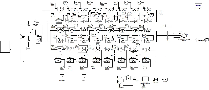
PROPOSED TOPOLOGY CONFIGURATION:
FIG:Three-phase power schematic of the proposed seventeen-level inverter
The voltages of capacitors AC1, BC1, and
CC1 are maintained at Vdc/2. Capacitors
AC2, BC2, and CC2 are maintained at
voltage level of Vdc/4. Similarly capacitors
AC3, BC3, and CC3 are maintained at
voltage level of Vdc/8 and capacitors AC4,
BC4, and CC4 are maintained at voltage
level of Vdc/16. The three-phase power
schematic is shown in Fig. 1. It consits of
hybrid multilevel topology employing a
three-level flying capacitor inverter and
cascading it with three floating capacitor
H-Bridges. Each cascaded H-bridge can either
add or subtract its voltage to the voltage
generated by its previous stage. In addition
to that, the CHBs can also be bypassed. The
resulting inverter pole voltage is the
arithmetic sum of voltages of each stage.
The schematic diagram for one phase of the
proposed converter is shown in Fig. 2. The
switch pairs (AS1, AS1’), (AS2, AS2’),
(AS3, AS3’), (AS4, AS4’), (AS5, AS5’),
(AS6, AS6’), (AS7, AS7’), and (AS8, AS8’)
are switched in complementary fashion with
appropriate dead time. Each switch pair has
two distinct logic states,
Fig. 2. One phase of the proposed
17-level inverter configuration formed by
cascading three-level flying capacitor
inverter with three H-bridges using a
single dc link.
namely top device is ON (denoted by 1) or
the bottom device is ON (denoted by 0).
Therefore, there are 256 (28) distinct
switching combinations possible. Each
voltage level can be generated using one or
more switching states (pole voltage
redundancies). By switching through the
redundant switching combinations (for the
same pole voltage), the current through
capacitors can be reversed and their voltages
can be controlled to their prescribed values.
This method of balancing the capacitor
voltages at all load currents and power
factors instantaneously has been observed
for 17 pole voltage levels. They are 0,
Vdc/16, Vdc/8, 3 Vdc/16, Vdc/4, 5 Vdc/16,
3 Vdc/8, 7 Vdc/16, Vdc/2, 9 Vdc/16, 5
Vdc/8, 11 Vdc/16, 3 Vdc/4, 13 Vdc/16, 7
Vdc/8, 15 Vdc/16, and Vdc. However, by
Available online: http://internationaljournalofresearch.org/ P a g e | 233
voltage switching combinations, 31 distinct
pole voltage levels can be generated using
the proposed topology. In the additional 14
levels, the voltages of capacitors can be
balanced only in a fundamental cycle. There
are 82 switching combinations (see Table I)
that can be used to generate the above
mentioned 17 pole voltage levels where
instantaneous capacitor voltage balancing is
possible. The effect of 82 switching
combinations on every capacitor’s charge
state (charge or discharge) for positive
direction of current (i.e., when the pole is
sourcing current as marked in Fig. 3)is
shown in Table I. For negative direction of
current, the effect of the switching state on
the capacitor is reversed. For example, when
the controller demands a pole voltage of
Vdc/16, there are five different redundant
switching combinations to generate it. Each
switching combination has a different effect
on the state of charge of the capacitors.
When the switching state (0, 0, 0, 0, 0, 0, 0,
1) (see Table I)is applied, the capacitor C4
discharges when the pole is sourcing current
as [see Fig. 3(a)]. To balance the capacitor
C4 and to bring its voltage back to the
prescribed value (Vdc/16), one of the other
four switching combinations is applied Fig.
3(b)–(e). It can be observed that when
switching state (0, 0, 0, 0, 0, 1, 1, 0) is
applied, the direction of current in the
capacitor C4 is reversed [see Fig. 3(b)] and
the capacitor C4 charges. However in this
process, the capacitor C3 is discharged. If
the capacitor C3 needs charging, switching
state redundancy of (0, 0, 0, 1, 1, 0, 1, 0) is
applied [see Fig. 3(c)] which discharges C2.
As shown in Fig. 3(d) to charge C2 one of
the switching redundancies and (e) is
applied based on the state of charge of
capacitor C1. If switching state (0, 1, 1, 0, 1,
0, 1, 0) is applied, the capacitor C1 is
discharged and this state charges all the
other capacitors as shown in Fig. 3(d).
Finally, when switching state of (1, 0, 1, 0,
1, 0, 1, 0) is applied, all the four capacitors
are charged for positive direction of current
as shown in Fig. 3(e).
(a)
(b)
(d)
(d)
Fig. 3. Switching Redundancies for pole voltage of Vdc/16. (a) Current path for switching state (0, 0, 0, 0, 0, 0, 0, 1). (b) Current path for switching state (0, 0, 0, 0, 0, 1, 1, 0). (c) Current path for switching state (0, 0, 0, 1, 1, 0, 1, 0). (d) Current path for switching state (0, 1, 1, 0, 1, 0, 1, 0). (e) Current path for switching state (1, 0, 1, 0, 1, 0, 1, 0).
TABLE I
POLE VOLTAGE REDUNDANCIES AND CAPACITOR STATES FOR VARIOUS SWITCHING COMBINATIONS WHEN POLE SOURCES CURRENT
Symbols of + , −, and 0 indicates the capacitor is charging, discharging, and no effect respectively for positive direction of current.
SIMULATION RESULT:
Available online: http://internationaljournalofresearch.org/ P a g e | 235
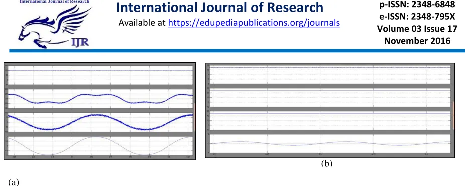
(a)
Fig. . Pole, Phase, capacitor voltages along with current for 10-Hz operation of converter. VAC1(50 V/div),VAO: Pole voltage (100 V/div), VAN: Phase Voltage (100 V/div), VAC4: (100 V/div),VAC3:
(10 V/div),VAC2: (25 V/div), IA:2 A/div, Timescale: (20 mS/div).
CONCLUSION
In the proposed configuration if any of the
devices in any of the H-bridges fail, the
faulty H- bridge are often bypassed and the
electrical converter can be operated at
reduced number of levels at full power. In
this paper a cascading a 3- level flying
capacitor and three floating capacitor
H-bridges has been formed for generating a 17
level configuration and the proposed
17-level inverter has improved reliability. The
advantage of the proposed configuration is
modularity and symmetry in structure with
the same control scheme which enables the
inverter to be extended to more number of
phases like five-phase and six- phase
configurations. At any power factor all the
voltage levels can be balanced in the
proposed system at full loads. The
performance can be observed in the
simulation. The stability of the capacitor
balancing algorithm has been tested by using
simulation suddenly accelerating the motor
at no load and observing the capacitor
voltages at various load currents.
REFERENCES
[1] J. Rodriguez, J.-S. Lai, and F. Z. Peng,
“Multilevel inverters: A survey of topologies, controls, and applications,”
IEEE Trans. Ind. Appl., vol. 49, no. 4, pp.
724–738, Aug. 2002.
[2] L. G. Franquelo, J. Rodriguez, J. I. Leon,
S. Kouro, R. Portillo, and M. A. M. Prats,
“The age of multilevel converters arrives,”
IEEE Ind. Electron. Mag., vol. 2, no. 2, pp.
28–39, Jun. 2008.
[3] S. Kouro, M. Malinowski, K.
Gopakumar, J. Pou, L. G. Franquelo, B.Wu,
J. Rodriguez, M. A.
[4] Y. Liang, C.O. Nwankpa, "A power-line
conditioner based on flyingcapacitor
phase-shift SPWM" IEEE Trans. Industrial
Electronics, Vol. 36, pp. 965-971, 2000.
[5] E. Villanueva, P. Correa, M. Pacas,
“Control of a Single-Phase Cascaded
H-Bridge Multilevel Inverter for
Grid-Connected Photovoltaic Systems”, IEEE
Trans. Industrial Electronics, Vol. 56, pp.
4399-4406, 2009.
[6] O. Lopez, R. Teodorescu, J.
Doval-Gandoy, "Multilevel transformerless
topologies for single-phase grid-connected
converters" IEEE. IECON 2006, pp.
5191-5196, 2006.
[7] Tae-Jin Kim, Dae-Wook Kang, Yo-Han
Lee and Dong-Seok Hyun, “The analysis of
conduction and switching losses in
multi-level inverter system”, PESC. 2001 IEEE
Vol. 3, pp 1363-1368, 2001.
[8] D.A.B. Zambra, C. Rech, J.R. Pinheiro,
"Comparison of Neutral-Point- Clamped,
Symmetrical, and Hybrid Asymmetrical
Multilevel Inverters", IEEE Trans. Ind.
Electron., Vol. 57, no. 7, pp2297-2306, July
2010.
[9] M. Calais, "Analysis of multicarrier
PWM methods for a single-phase five level
inverter", PESC. 2001 IEEE, Vol. 3, pp.
1351-1356, 2001.
[10] B.P. McGrath, “Multicarrier PWM
strategies for multilevel inverters”, IEEE
Trans. Ind. Electron., Vol. 49, no. 4, pp.
858-867, 2002.
[11] G. Carrara, S. Gardella, M. Marchesoni,
R. Salutari, and G. Sciutto, "A new
multilevel PWM method: A theoretical
analysis", IEEE Trans. Power Electron., vol.
7, no. 3, pp. 497-505, July 1992.
AUTHOR’S PROFILE:
G. Nirosha
Available online: http://internationaljournalofresearch.org/ P a g e | 237