Design of High Frequency 16/17 Dual Modulus
Prescaler Using TSPC Flip Flop
Mohammed Salih, Rohini K
Assistant Professor, Dept. of ECE, Government Engineering College, Idukki, Kerala, India1
PG Student [VLSI and Embedded System], Dept. of ECE, Government Engineering College, Idukki, Kerala, India2
ABSTRACT: A high speed and high frequency CMOS TSPC based divide-by-16/17 dual modulus prescaler is
proposed. Dual-modulus prescaler is implemented without using any extra logic gates by exploiting the special feature of the TSPC flip-flop. The speed of the prescaler is improved in two aspects. First, by adopting a new pseudo divide-by-2/3 prescaler, the minimum working period is effectively reduced by half a NOR gates delay. Second, by changing the connection of TSPC D-Flip-Flops, the minimum working period is further reduced by half an inverters delay. Designed in 180-nm CMOS process, the proposed circuit is capable of operating up to 6.5 GHz. The power consumption is 3.25 mW at the maximum operating frequency under 1.6 V supply voltage.
KEYWORDS: Dual modulus, Prescaler, Divide-by 2/3,TSPC
I.INTRODUCTION
The rapid evolution of the communications industry has increased the demand for low cost, low power and wide bandwidth RF circuits. Today's technologies make possible powerful computing devices with multi-media capabilities. Consumer's attitudes are gearing towards better mobilityandaccessibility. This caused a demand for an ever-increasing number of portable applications requiring low-power and high throughput.Intensive efforts are made to develop RF circuitsoperating at GHz range using low-cost CMOS process. Low power consumption is required to increase the battery life time and to reduce the operating temperature.
Frequency dividers,also known as prescalers are used in many communications applicationssuch as frequency synthesizers, timing-recovery circuits and clock generation circuits. It is one of the most critical block in the frequency synthesizer because it operates at the highest frequency and consumes large power. Thus the power reduction in the first stage
of the prescaler is important in realizing a low power frequency synthesizer.High speed dual-modulus frequency prescalers
have an important role in phase-locked loop (PLL) designs too[1] - [4].They allow multiple division ratios using a single divider. Power consumption,speed and maximum operating frequency are the major factors to be considered while designing a dual modulus prescaler.
II.RELATED WORK
design rules of TSPC circuits are broken. It leads to shrinking frequency range because these prescalers are no longer suitable for low frequency operation.
Today both the divide-by-2/3 and divide-by-4/5 prescaler are most widely utilized. Usually, divide-by-2/3 prescaler has the advantage of speed more than divide-by-4/5 and these prescaler is more power efficient too. Thus, divide-by- 2/3 prescaler is preferred in 16/17 prescalers. On the other hand, divide by 4/5 prescaler is preferred in applicationswhere large division ratio is required, such as 128/129 prescalers and it helps to minimize the critical path.
In this brief, two aspects can improves the maximum working frequency of the divide-by-16/17 prescaler. First, develop a new pseudo divide-by-2/3 prescaler and adoptedinto the divide-by-16/17 prescaler, which leads to reduce the minimum working period by half a NOR gates delay. Second, the minimum working period is further reduced by half an inverters delay, by changing the connection of efficient TSPC D-flip-flops (DFFs).
III. TSPC D FLIP FLOP
D-flipflop is the data flip flop transfers the data withoutany flipping.A high-speed TSPC DFF proposed is shown in Fig. 1, where clock-controlled transistors are placed close to a power supply line to increase switching speed.The setup time of the TSPC DFF can be written as
tsetup = tD-S
Where tD-Smeans the propagation time from node D to node S, which is a clocked inverters delay. The propagation
delay of the TSPC DFF can be written as tD-Qn= tS-T+ tT-Qn
Where tD-Qn is the propagation delay from CLK to Qn. tS-T and tT-Qn represents the propagation delay from node S to T, T
to Qn respectively. One inverter stage is required at node Qn to get the correct Q output.
An advantage of TSPC circuits is that AND/OR logic gates can be absorbed into the first stage of TSPC DFFs and the logic depth can be reduced [9]. After AND/OR gate absorption, the first stage of the TSPC DFFs will become a clocked NAND/NOR gate. The logic depth can be reduced by about two inverters delay after absorption.
Figure 1: Structure of TSPC DFF.
IV. CONVENTIONAL DIVIDE-BY-16/17DUAL-MODULUS PRESCALER
Within a period of Fin, signal must pass path #1 while within a periods of Fin it should pass path #2.theoritically, it is critical to identify which path decides the minimum working period. But the result varies in different designs. In conventional divide by 16/17 prescaler there is a trade-off between lengths of the two critical paths. The optimized design is to make the length of critical path #1 approximately equal to half length of critical path #2. In conventional divide-by-16/17 prescaler, In front of DFF0 two logic gates (NAND and OR1) are located. In addition, there are two critical paths. Apparently, it is not the optimized design.To achieve a high speed both the critical paths should be optimized, which is a great challenge for designers.
Fig.2: Schematic of conventional divide-by-16/17 prescaler.
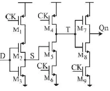
V. PROPOSED DIVIDE-BY-16/17 DAUL MODULUS PRESCALER
Function of three branches of TSPC flip flop shown inFig.1 is as follows. The first branch samples input data when CK = 0 (negative cycle) and holds the data when CK = 1 (positive cycle), the second branch precharges node T during the negative clock cycle and evaluates the data during the positive cycle, and the third one passes the evaluated data during the positive cycle and holds the output during the negative cycle. Therefore, the evaluation result in the second branch decides the output of the DFF. When the input is high, the charge on the node T holds, and output Qn goes low immediately after the clock rises high. On the other hand, when the input is low, the node T has to be discharged before Qn goes high, which inherently limits the speed of TSPC operation. Since the second branch works as a domino logic, adding a transistor to the node T creates a NOR logic gate that can change the output value without passing through the first branch. We exploit this behavior to design high-speed dual-modulus prescalers.
Fig. 3 shows a new 2/3 prescaler by adding NOR gate to node T. Here the separated logic gates in conventional design are removed, and the two transistors Ma1 and Mc1 are added to implement a NOR gate at the node T1. When set to a divide-by-2 mode, the control signal MC is low, and the added transistors do not affect the behavior of the node T1, except for adding a small capacitive load. When MC goes high, the path from the output of the DFF2 to the node T1 is enabled. Once Qn2 goes high, the added path forces T1 to logic low and extends the high level of the output Qn1; therefore, the division ratio becomes 3.
In divide by 2 operation, the circuit is identical to asingle TSPC flip flop except a small parasitic capacitance at node T.Hence the operating speed is closer to that of a single TSPC flip flop. During divide by 3 operation, since Qn2 skip first branches in DFF1 and forces node Qn1 to low directly,operating speed is even faster than divide by 2 operation.
Fig.4: Schematic of proposed 16/17 prescaler.
This 2/3 prescaler is used to implement 16/17 prescaler. Schematic of 16/17 dual modulus prescaler using the above 2/3 prescaler is shown in Fig.4. The operation mode of proposed circuit is as follows. When MC = 1, MC1 changes its value according to (QN2, QN3, QN4). The pseudo divideby- 2/3 prescaler controlled by MC1 accomplishes seven times of divide-by-2 operations and one time of divide-by-3 operation in a cycle. The whole circuit operates in divideby- 17 mode. When MC = 0, MC1 keeps low and the pseudo divide-by-2/3 prescaler keeps on divide-by-2 operation. The whole circuit works in divide-by-16 mode.
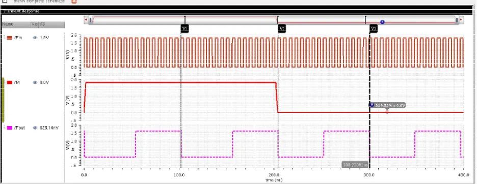
VI. MEASUREMENT RESULTS
The proposed divide-by-16/17 prescaler is designed in 180 nm CMOS technology. Output waveform of 16/17 prescaler is shown in Fig.5. Measurement results show thatthe proposed circuit achieves a maximum working frequency of 6.5 GHz under 1.6 V supply voltage.
Table I shows the comparison of conventional 16/17 prescaler with the proposed prescaler. Power, delay and number of transistors are less for the proposed design.
Table I: Comparison of proposed circuits with conventional system
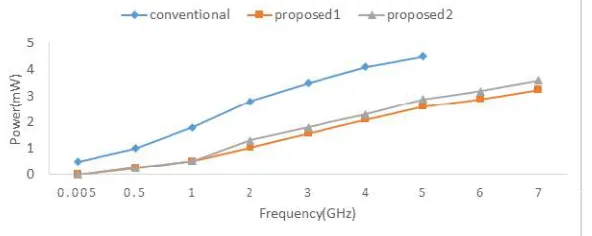
Fig. 6 shows the frequency Vs power graph of conventional prescalerand the proposed prescalers. Power increases linearly with input frequency and reaches 3.25mW at maximum working frequency (6.5 GHz) and for conventional design it is 4.5 mW.
Fig.6: Frequency Vs Power consumption.
Layout of the proposed 16/17 prescaler is shown in Fig.7.
VII.CONCLUSION
This brief presents a novel high speed TSPC divide-by- 16/17 dual modulus prescaler. The proposed circuit reduces and power and increases the speed of operation which inturn increases the maximum operating frequency. The speedof prescaler is improved in two aspects. First is by adopting a new pseudo divide-by-2/3 prescaler. Second is by changing the connection of TSPC D-Flip-flops, i.e., by avoiding the fourth stage in TSPC flip flop, the minimum working period is reduced by half an inverters delay. Designed in 0.18um CMOS technology, the proposed circuit achieves a 6.5 GHz maximum working frequency.
REFERENCES
[1] T. Shibasaki, H. Tamura, K. Kanda, H. Yammaguchi, J. Ogawa, and T. Kuroda, “A 20-GHz injection-locked LC divider with a 25range,” Int. Symp. VLSI Circuits Dig. Tech. Papers, Jun. 2006, pp. 170171.
[2] D. D. Kim, J. Kim, and C. Cho, “A 94GHz locking hysteresis assisted and tunable CML static divider in 65nm SOI CMOS,” IEEE ISSCC Dig. Tech. Papers, Feb. 2008, pp. 460628.
[3] B. Chang, J. Park, and W. Kim, “A 1.2 GHz CMOS dual modulus prescaler using new dynamic D-type flip-flops,” IEEE J. Solid-State Circuits, vol. 31, no. 5, pp. 749752, May 1996.
[4] C.-Y. Yang, G.-K. Dehng, J.-M. Hsu, and S.-I. Liu, “New dynamic flip-flops for high-speed dual-modulus prescaler,” IEEE J. Solid-State Circuits, vol. 33, no. 10, pp. 15681571, Oct. 1998.
[5] S. Kim and H. Shin, ”An E-TSPC divide-by-2 circuit withforward body biasing in 0.25 m CMOS,” IEEE Microw.Wireless Compon. Lett., vol. 19, no. 10, pp. 656658, Oct.2009.
[6] H. Shin, ”A 1-V TSPC dual modulus prescaler with speedscalability using forward body biasing in 0.18 m CMOS,”IEEE Trans. Circuits Syst. I, Reg. Papers, vol. 57, no. 1, pp.7282, Jan. 2010.
[7] M. V. Krishna, M. A. Do, K. S. Yeo, C. C. Boon, and W.M. Lim, ”Design and analysis of ultra-low power true singlephase clock CMOS 2/3 prescaler,” IEICE Trans. Electron.,vol. E95-C, no. 6, pp. 11211124, Jan. 2012.
[8] W.-H. Chen and B. Jung, ”High-speed low-power true singlephaseclock dual-modulus prescalers,” IEEE Trans. CircuitsSyst. II, Exp. Briefs, vol. 58, no. 3, pp. 144148, Mar. 2011.
[9] J. M. Rabaey, A. Chandrakasan, and B. Nikolic, “DigitalIntegrated Circuits: A Design Perspective,” 2nd ed. New York,NY, USA: Prentice- Hall, 2003, pp. 350352.
[10] X. P. Yu,W. M. Lim, M. A. Do, X. L. Yan, and K. S. Yeo, “6.1GHz 4.6 mW CMOS divide-by-55/56 prescaler,” Electron.Lett.,vol. 44, no. 24, pp. 14021403, Nov. 2008.
[11] V. K. Manthena, M. V. Do, C. C. Boon, and K. S. Yeo, “A low-power single-phase clock multiband flexible divider,”IEEE Trans. Very Large Scale Integr. (VLSI) Syst.,vol. 20, no.20, pp. 376380, Feb. 2012.