A Modified High Frequency Link
Bidirectional Inverter Based on Switched
Capacitor Resonant Converter
D.Nirmala
1, Dr.C.Vivekanandan
2, N.Rajesh
3PG student [PED], Dept. of EEE, SNS college of Engineering, Coimbatore, Tamilnadu, India1 Professor& Vice Principal, SNS college of Engineering, Coimbatore, Tamilnadu, India2 PG student [PED], Dept. of EEE, SNS college of Engineering, Coimbatore, Tamilnadu, India3
ABSTRACT: In this work, a switched capacitor resonant converter based bidirectional High Frequency Link (HFL) inverter is proposed to convert low level DC voltage from sources such as batteries, fuel cells etc. to AC. The inversion of low voltage DC power is accomplished in two steps. The first step is being the conversion of the low voltage DC into a high voltage DC and the second step is the conversion of high DC source to an AC waveform using pulse width modulation and bidirectional operation is ensured by a proper selection of the dc-dc resonant converter. Flyback converter is used as a high frequency link, which provides proper isolation. The switching frequency of the converter is set to 20 kHz for faster switching operation. This system is simulated in MATLAB software. As a result of incorporating a resonant converter topology, the switching device count is reduced, complexity in the control strategy is lesser comparing a conventional type and therefore, switching losses are minimized. Due to this the total harmonic distortion is brought down to 0.83% which results in an overall better performance of the inverter.
KEYWORDS
:
High Frequency Link (HFL), Flyback converter, Resonant converter, Pulse Width Modulation (PWM), Total Harmonic Distortion (THD).I.INTRODUCTION
The need to have compact size and reduced weight gadgets, without compromising efficiency, cost and reliability, forces the devices to operate with high power density. High Frequency Link (HFL) power converters are one of the strategies to address the above issue and the benefits of high frequency converters have been recognized and their importance has significantly increased [7]. The merits of HFL inverter are widely recognized, and its application has covered areas such as Uninterruptible Power Supply (UPS) and Renewable Energy source systems [9]. Compared to the conventional Pulse Width Modulation (PWM) inverter, the HFL inverter offers reduction in size and weight, due to the absence of line-frequency (50Hz) transformer. The two well-known HFL inverters are the “Cycloconverter” and the “DC to DC type converter”.
The achievement of high power densities at high switching frequency and high efficiency levels represents a challenging issue for power converter designers and from literature it is found that soft switching (ZVS/ZCS) methods can mitigate some of the mechanisms of switching loss and possibly reduce the generation of EMI. Remarkable efforts have been made in the development of high-frequency zero-voltage switching (ZVS) and zero-current switching (ZCS) dc-ac power converters. In these converters, the principle of resonance is used to implement the soft-switching techniques (ZVS/ZCS) [6]. Resonant converters use a resonant circuit for switching the devices at zero current or at zero voltage as this reduces the stress on the switching devices and the radio interference. Many control methods have been suggested for controlling the resonant converter and each method has its own advantages and drawbacks, due to which a particular control method is considered suitable under specific conditions, compared to other control methods. However, a control method that gives the best performances under any conditions is always in demand.
number of switching devices and soft switching methods leads to less switching losses resulting reduction in total harmonic distortion. Figure 1 shows the block diagram of the proposed inverter
Figure 1: Block Diagram of the HFL Inverter
The flyback converter is fed from a DC source and flyback converter is used to boost the input DC voltage. The boosted voltage is flows through the Switched capacitor resonant converter which act as a DC-DC converter and the PWM inverter converts the DC voltage from the resonant converter to an AC.
II.LITERATURE SURVEY
Chen D and Chen Y, “Step-up AC voltage regulators with high-frequency link”, IEEE Transactions on Power Electronics, vol. 28, no. 1, pp. 390–397, January. 2013. In this paper the proposed ac voltage regulators with HFL can convert an unstable sinusoidal voltage with THD to a stable sinusoidal voltage with the same frequency and low distortion. The instantaneous voltage feedback strategy with phase shifted control is introduced in this regulators [2]. The automatic input voltage zero-crossing start-up circuit can avoid the magnetic saturation when the regulators start to work. The active clamped circuit can effectively suppress the voltage spike caused by the leakage inductance of the HF transformer.
De D. and Venkataramanan R, “Analysis, design, modeling, and implementation of an active clamp HF link converter”, IEEE Transactions on Industrial Electronics, vol. 58, no. 6, pp. 1146–1155, June. 2011. In this paper the system oriented analysis of the active clamp circuit during rectifier and inverter mode of operation of the power circuit are discussed. The design procedure to select snubber circuit parameters for a dc- HF link power converter is not straight forward [1]. An approximate design procedure is carried out to select the snubber capacitor value and the on-time of the active device. The suitable switching instant of the snubber device is identified for safe operation of the power circuit.
Krein P.T, Balog R. S, and Geng X, “High-frequency link inverter for fuel cells based on multiple-carrier PWM”, IEEE transactions on Power Electronics vol. 19, no. 5, pp. 1279–1288, September. 2004. In this paper the fuel cell based converter is focused as the Fuel cells are well-suited to current-sourced converters because of their control requirements and low tolerance for mains-frequency ripple. It was shown that the number of stages can be reduced, leading to a HF-link conversion approach. The reduction came from recognizing redundancy in the power processing. Without a dc link bus, rectifiers and filter components along with their associated losses were eliminated [7]. Applying the techniques of PWM cyclo conversion resulted in a PWM output exactly identical to conventional PWM techniques. From the above survey the following points are observed with respect to the benefits of HFL inverters:
Reduced size and weight.
Provides high degree of isolation between input and output.
In low cost medium power applications, HFL inverters significantly reduce the switching device count and number of power processing stages.
III. PROPOSED HIGH FREQUENCY LINK INVERTER
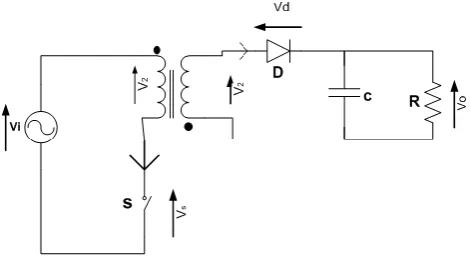
The conventional DC to DC type high frequency link inverters consist of three power stages, the HF PWM Bridge, active rectifier and polarity-reversing bridge. In this work DC to DC type HFL inverter with two stage conversion is achieved by using a fly back converter, which is used as a high frequency link. The flyback converter is used in both AC to DC and DC to DC conversion with galvanic isolation between input and any outputs. The fly back converter is a buck- boost converter with a inductor split to form transformer, so that the voltage ratios are multiplied with an additional advantage of isolation. Figure 2 shows the schematic of flyback converter.
When switch „S‟ is on, the primary winding of the transformer gets connected to the input supply with its dotted end connected to the positive side. At this time the diode „D‟ connected in series with the secondary winding gets reverse biased due to the induced voltage in the secondary (dotted end potential being higher). When Switch turns off, the current in the primary winding drops suddenly, the voltage across the primary winding reverses. The diode becomes forward biased.
Figure 2: Flyback converter
If the off period of the switch is kept large, the secondary current gets sufficient time to decay to zero and magnetic field energy is completely transferred to the output capacitor and load. One of the major advantages of fly back converter is that they doesn‟t require an output filter inductor. This also makes flyback converters valuable for high output voltages unlike forward converter which have an output inductor potentially causing problems as the inductor must sustain large voltages. Flyback also don‟t require a high voltage freewheeling diode.
The filter capacitor at the output is typically larger in flyback converters as it alone supplies the load current when the switch is ON. Equivalently the full DC current flows from ground through the capacitor to the load during the ON time. Thus the ripple current rating of the capacitor and the output ripple voltage requirement collectively determines the final choice of the output filter.
IV.CIRCUIT ANALYSIS
D 1
C1
LR
S1 CR
DC input
S2
S3
S4
S5 C2
S6 S8
S7 S9
R load Flyback
converter
Switched capacitor
Resonant converter PWM inverter
Figure 3: Circuit diagram of the HFL inverter
The SCRC consists of two half-bridge inverters with four switching devices S2-S5 and a series resonant circuit Lr and Cr
. Addition of the small inductor is the difference from a conventional SCC in the circuit configuration, resulting in a great suppression of spike currents, power losses, and EMI issues. Each switch in the resonant converter is formed by back to back connected MOSFETs.
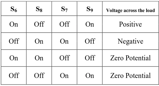
The H bridge inverter followed by the resonant converter is a switching configuration composed of four switches in an arrangement that resembles an H. By controlling different switches in the bridge, a positive, negative, or zero potential voltage can be placed across a load. The switching position of a H bridge inverter are outlined below in table 1
Table 1: Switching States of H Bridge inverter
V.SIMULATION AND RESULTS
The simulation of the proposed HFL inverter with closed loop control is presented along with the simulation results. MATLAB-Simulink is used to simulate the proposed inverter with different input DC values. The waveforms at various stages are observed and given along with the analysis. It is observed that the performance of the inverter is improved than the previous work and the control schemes incorporated are simpler. The total Harmonic Distortion (THD) is 0.83% which is very less compare to the existing work. The input for the proposed model is 50 V DC and the output is a variable AC with a range of 0-150V.
S
6S
8S
7S
9 Voltage across the loadOn
Off
Off
On
Positive
Off
On
On
Off
Negative
On
On
Off
Off
Zero Potential
Specifications:
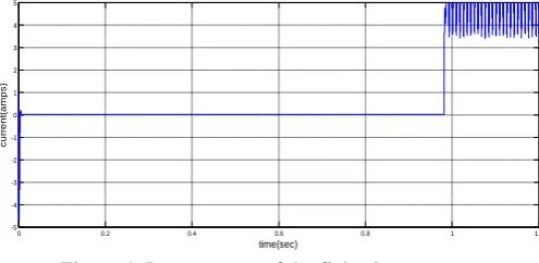
The input voltage given to the flyback converter is 50V DC and obviously at this instance no switch is provided with any gate pulses resulting zero input current. Once the gating signals are given the functioning of the flyback converter starts and the corresponding input current patterns are as given in Figure 4. From Figure 4 it is observed that the input current is zero till 0.8 sec which implies that gating pulses are not given to the converter switches till that period and load is not connected to the circuit. But the voltage across the back to back connected converter switches increases rapidly due to over modulation.
Figure 4: Input current of the flyback converter
Since it is a closed loop system, the voltage variations are sensed and maintained in a constant value after 1 sec, i.e. after settling period by controlling the gate pulses given to the switch S1 and the measured input current at this instant is
5A. The switched capacitor resonant converter followed by the flyback converter is operating as a dc to dc converter. This either boosts or bucks the applied dc voltage according to the load requirements. If the output voltage from the PWM inverter exceeds the load requirement, the resonant converter act as a buck converter and if the output voltage from the PWM inverter is less than the load requirement, it acts as a boost converter by controlling the gate pulses given to the switches in the resonant converter.
Figure 5: Load voltage of the HFL inverter
The MOSFETs of resonant converter circuit are switched on or off in accordance with the gating signals received from
0 0.2 0.4 0.6 0.8 1 1.2
-5 -4 -3 -2 -1 0 1 2 3 4 5
time(sec)
c
u
rr
e
n
t(
a
m
p
s
)
used to control the gate pulses. The amount of ripple content in the inverter voltage decides the filter choice. Since the ripples in the output voltage are less due to the proper switching and converter control methods, an inductive filter is sufficient to filter the ripples. After the choice of 5 mH inductive filter, the ripples in the output voltage and current are filtered out
Figure 6: Load current of the HFL inverter
. Figure 5,6 shows the load voltage and current. The load voltage is obtained by converting peak voltage to the rms voltage and then plotted .The output power calculated is 225W.
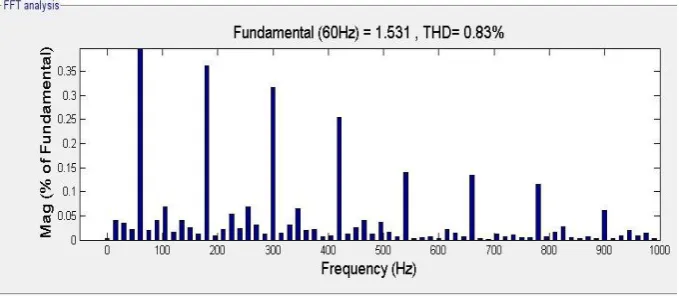
THD ANALYSIS OF THE HFL INVERTER
Figure 7: THD analysis of the HFL inverter
From the THD analysis, it may be concluded that the THD is very less. The reduction in the THD ensures the better performance of the inverter.
VI.CONCLUSION
REFERENCES
[1] Chen D and Chen Y, “Step-up AC voltage regulators with high-frequency link”, IEEE Transactions on Power Electronics, vol. 28, no. 1,
pp. 390–397, January. 2013.
[2] Chung Y. H, Shin B.S, and Cho G. H, “Bilateral series resonant inverter for high frequency link UPS”, in proceeding of the IEEE Power
Electronics Specialists conference., vol. 38, no. 4, pp. 159–166, July. 1991.
[3] De D. and Venkataramanan R, “Analysis, design, modeling, and implementation of an active clamp HF link converter”, IEEE
Transactions on Industrial Electronics, vol. 58, no. 6, pp. 1146–1155, June. 2011.
[4] Inoue S and Akagi H, “A bidirectional DC–DC converter for an energy storage system with galvanic isolation”, IEEE transactions on
Power Electronics, vol. 22, no. 6, pp. 2299–2306, Nov.2007.
[5] Javier Pereda and Juan Dixon, “High-Frequency Link: A Solution for Using Only One DC Source in Asymmetric Cascaded Multilevel
Inverters”, IEEE transactions on Industrial Electronics, vol. 58, no. 9, September. 2011.
[6] Kenichiro Sano and Hideaki Fujita, “Performance of a High-Efficiency Switched-Capacitor-Based Resonant Converter With Phase-Shift”,
IEEE Transactions on Power Electronics, vol. 26, no. 2, February. 2011.
[7] Krein P.T, Balog R. S, and Geng X, “High-frequency link inverter for fuel cells based on multiple-carrier PWM”, IEEE transactions on
Power Electronics vol. 19, no. 5, pp. 1279–1288, September. 2004.
[8] Lu W, Zhou K, Wang D, and Cheng M, “A general parallel structure repetitive control scheme for multiphase DC–AC PWM converters”,
IEEE Transactions on Power Electronics, vol. 28, no. 8, pp. 165–175, January. 2013.
[9] Mazumder S. K and Rathore A. K, “Primary-side-converter-assisted soft-switching scheme for an AC/AC converter in a
cycloconverter-type high-frequency-link inverter”, IEEE transactions on Industrial Electronics, vol. 58, no. 9, pp. 4161–4165, September. 2011.
[10] Wenjie Zhu, Keliang Zhou, and Ming Cheng, “A Bidirectional High-Frequency-Link Single phase Inverter: Modulation, Modeling, and