ABSTRACT
SINGH SHRISHTI. A Novel DC Circuit Breaker with Artificial Zero Current Interruption. (Under the direction of Dr. Subhashish Bhattacharya and Dr. Leonard White).
The thesis focuses on developing a low voltage prototype of a medium voltage DC Circuit Breaker. Dr. Leonard White P.E and Dr. Subhashish Bhattacharya patented the unique concept. This thesis thus discusses the existing issues with DC current interruption and proposes a novel solution.
Based on the proposed concept, circuit simulations were done on PLECS to verify the operation of the system with the selected components. A mathematical analysis of the circuit was done and the expression for short circuit protection time is evaluated. The hardware set up and testing was performed in FREEDM Systems Center lab. The circuit was tested up to 40 VDC to achieve the expected results. The analytical expressions were verified from the experimental values. The setup uses 1.2 kV IGBT switches, a 230V 1kVA isolation transformer and 4.7 mF Capacitor.
A Novel DC Circuit Breaker with Artificial Zero Current Interruption
by Shrishti Singh
A thesis submitted to the Graduate Faculty of North Carolina State University
in partial fulfillment of the requirements for the degree of
Master of Science
Electrical Engineering
Raleigh, North Carolina 2019
APPROVED BY:
_________________________ _________________________
Dr. Subhashish Bhattacharya Dr. Leonard White
Committee Chair
ii
DEDICATION
To my parents,
Late Anita Singh
AND
iii
BIOGRAPHY
iv
ACKNOWLEDGEMENTS
Firstly, I would like to thank my advisor Dr. Subhashish Bhattacharya for providing me with this great opportunity and for his support and encouragement. This opportunity introduced me to the world of research and innovation and instilled in me a quest for learning more. I would also like to extend my heartfelt gratitude towards Dr. Leonard White P.E and for all the interactive and informative discussions that kept me constantly motivated. I am very proud to have successfully build the first prototype of the patented technology.
I would especially like to thank my mentor Ashish Kumar who has been a constant pillar of support throughout the graduate school journey. I would like to thank my friends Siddharth Khandelwal, Aishwarya Ravichandran and Tejal Ghongadi.
v
TABLE OF CONTENTS
LIST OF TABLES...vii
LIST OF FIGURES ... viii
Chapter 1: DC Circuit Breaker Overview ... 1
1.1. Background ... 1
1.2. Motivation... 2
1.3. Literature Review ... 2
1.4. Scope ... 6
Chapter 2: Proposed DC Circuit Breaker ... 8
2.1. General description of the Patent ... 8
2.1.1. Operational Details... 10
2.1.2. Initial pre-trip conditions ... 10
2.1.3. Trip Action ... 11
2.2. Controller Design for the Proposed DCCB ... 11
2.3. Theoretical Analysis ... 13
Chapter 3: Modeling and Simulation ... 18
3.1. Circuit Modeling ... 18
3.2. Results ... 20
Chapter 4: Hardware Design ... 22
4.1. Component Selection ... 22
4.1.1. Power Circuit ... 22
4.1.2. Control Circuit ... 23
4.2. Control Circuit Design ... 24
4.2.1. Schematic ... 24
4.2.2. PCB Layout ... 25
Chapter 5: Experimental Results ... 26
5.1. Transformer Testing ... 26
5.1.1. Open Circuit Test ... 27
5.1.2. Short Circuit test... 28
vi
5.3. Transformer Action Test... 29
5.4. Control circuit testing ... 31
5.5. Current Sensor testing ... 32
5.6. Measurement instruments and Supplies ... 32
5.7. Hardware Assembly ... 33
5.8. Challenges... 34
5.8.1. Ground Reference for Switches ... 34
5.8.2. Current Sensor ... 34
5.9. Short Circuit Protection Test ... 35
5.9.1. Results ... 36
5.9.2. Verification of Analytical Expression ... 39
Chapter 6: Conclusion ... 40
6.1. Summary ... 40
6.2. Scope of Improvements ... 40
vii
LIST OF TABLES
Table 1: Summary of Evaluated DC Circuit Breakers. ... 5
Table 2: Control Circuit Output. ... 12
Table 3: Circuit specifications of Main Circuit. ... 18
Table 4: Circuit specifications of secondary circuit. ... 18
Table 5:Components of Power Circuit. ... 23
Table 6: Components for Control Circuit. ... 23
Table 7: Transformer specification... 26
Table 8: Open Circuit Results. ... 27
Table 9: Open Circuit Test Results... 28
Table 10: Parameters of Transformer Action Test. ... 29
Table 11: Current Sensor Calibration. ... 32
Table 12: DC Sources... 33
Table 13: Oscilloscope. ... 33
viii
LIST OF FIGURES
Figure 1: Schematic of mechanical resonance DC Circuit Breaker [3]. ... 3
Figure 2: Schematic of the full Solid State Circuit Breaker [3]... 3
Figure 3: Schematic of the hybrid Solid State Circuit Breaker with fast mech switch [3]. ... 4
Figure 4: Schematic of the hybrid Solid State Circuit Breaker with fast mech dis-connector [3]. . 5
Figure 5: Solid State FID topology [4]. ... 6
Figure 6: DC Circuit Breaker. ... 8
Figure 7: Proposed DC Circuit Breaker Topology [1]. ... 8
Figure 8: DC Circuit Breaker electrical diagram. ... 10
Figure 9: Control Circuit. ... 12
Figure 10: DC Circuit Breaker Circuit Diagram. ... 13
Figure 11: Timing diagram of expected current waveform. ... 14
Figure 12: Equivalent Circuit Diagram - Phase I. ... 15
Figure 13: Equivalent Circuit Diagram of Phase II. ... 15
Figure 14: Equivalent Circuit Diagram - Phase III... 16
Figure 15: Equivalent Circuit Diagram Phase IV. ... 17
Figure 16: DC Circuit Breaker PLECS model... 19
Figure 17: Control circuit subsystem on PLECS. ... 19
Figure 18: Waveform results of PLECS simulation. ... 20
Figure 19: Proposed hardware design. ... 22
Figure 20: Schematic drawing of Control Circuit on EAGLE. ... 24
Figure 21: PCB layout on EAGLE. ... 25
Figure 22: Soldered PCB... 25
Figure 23: Transformer. ... 26
Figure 24: (a) Open Circuit Setup (b) Open Circuit 1 Winding. ... 27
Figure 25: (a) Short Circuit Setup (b) Short Circuit two winding. ... 28
Figure 26: Basic Proof of Concept circuit... 30
Figure 27: Primary and secondary current waveform. ... 30
Figure 28: Primary Current and Primary transformer Voltage. ... 31
Figure 29: Secondary Current and Capacitor Voltage. ... 31
ix
Figure 31: Hardware Setup for DC Circuit Breaker. ... 33
Figure 32: Hardware Setup. ... 34
Figure 33: Circuit Diagram for Short Circuit Protection Test. ... 36
Figure 34: Primary current. ... 37
Figure 35: Primary current and Breaker voltage. ... 37
Figure 36: Primary current and Secondary current. ... 38
1
Chapter 1: DC Circuit Breaker Overview
1.1. Background
A Circuit Breaker is essentially a switch used to interrupt current and is operated during fault conditions or sustained overloads in a power system. Its primary objective is to protect the loads as well as the system itself from high currents. Existing technologies for AC (Alternating Current) current interruption take advantage of the periodic zero crossing inherent to sinusoidal waveforms. In the case of DC (Direct Current) current, lack of zero crossing makes DC current interruption challenging.
There exist various types of circuit breakers like thermal circuit breakers, electromagnetic breakers, and solid-state breakers. These are differentiated based on the principle of operation. The most widely and traditionally used thermal breakers use a bimetallic strip, which melts due to the heat, produced by high fault currents and therefore break the circuit. Although the principle is simple, thermal breakers have a significantly high operating time making it unreliable and making replacement of the bimetallic strip inconvenient.
Electromagnetic breakers use a coil through which current flows, when the current exceeds the given limits, the electromagnet attracts the metal armature and the current is interrupted. The operating time of such breakers are relatively better than the former, yet they are not fast enough for many applications. The solid-state breakers use solid-state switches (MOSFETs, IGBTs) by giving required gate pulses to interrupt the current. With the least operating time, these are the most reliable but with a considerable loss of energy.
2
1.2. Motivation
With the increase of distributed energy resources in the modern grid, independent or grid-tied, the importance of DC switching has become an urgent need. From general application in the power distribution world including low voltage applications in Photovoltaic (PV) generation resources, energy storage application, to transmission and distribution applications at the Medium Voltage (MV) and High Voltage (HV) levels.
DC current lacks zero crossing therefore, faults happening in DC systems have the potential of being much worse than in its AC counterpart. Due to this and the fact that MVDC systems, in particular, have short line distances meaning low line inductance, DC faults can potentially cause severe damage to equipment if not handled correctly [2]. The patent technology presented in [1] targets both the solution to the later problem of DC interruption as well as the formerly mentioned growing need.
1.3. Literature Review
One of the main issues related to high power DC grids and DC transmission is the limited technology for current interruption. Presently the challenge is the short circuit current handling capability of current limiting devices and circuit breakers. With an inherent periodic zero crossing in AC current, there is a structural difference between the AC and DC mechanical circuit breakers. Since DC current has no natural zero crossing, it is imperative to create an artificial zero crossing at which the mechanical breaker should be opened. There is also a requirement of a very quick interruption with the dissipation of large amount of energy stored in the system inductances. DC breakers are widely available for the low and medium voltage range, but for High Voltage Direct Current (HVDC) applications, the breakers are not readily available in the market.
3
Mechanical Resonance DC Circuit Breaker: This breaker shown in Figure 1 creates an artificial zero current by superposing an oscillating current on the DC current [3]. In order to create the artificial zero crossing an LC series resonance circuit is connected in parallel with the mechanical breaker.
Figure 1: Schematic of mechanical resonance DC Circuit Breaker [3].
The inductance (L) and capacitance (C) are such selected that the oscillating current (LC - Resonance Path Current) is greater than the DC current passing through the mechanical breaker. Therefore, the superimposed current is the summation of the oscillating current and the DC current and produces zero current in the mechanical breaker, which is utilized to extinguish the DC arc.
Full Solid State Circuit Breaker: This configuration does not aim to create an artificial zero crossing and consists of solid-state devices (IGBTs, MOSFETs) in series with surge arrestors in parallel as shown in Figure 2.
4 The solid state devices are turned off when the fault current is detected, therefore the current flows through the surge arrestors and falls down to zero after few microseconds. The energy of system inductances is dissipated in the surge arrestors. Under steady state, condition the load current flows through the solid-state switches. The switches are subjected to a very high blocking voltage and thus devices with such high ratings tend to have a very high on resistance, resulting in higher losses.
Hybrid Solid State Circuit Breaker: This topology can have two types, one with a fast mechanical switch shown in Figure 3. In this topology under steady state condition, the load current flows through the fast mechanical switch, while the solid state switches remain off.
At the time of fault, the switches are turned on and fast mechanical switch is opened simultaneously. Therefore, the switches are subjected to a high blocking voltage whereas the fast mechanical switch with negligible contact resistance carries the load current under steady state condition.
Figure 3: Schematic of the hybrid Solid State Circuit Breaker with fast mech switch [3].
5 Figure 4: Schematic of the hybrid Solid State Circuit Breaker with fast mech dis-connector [3].
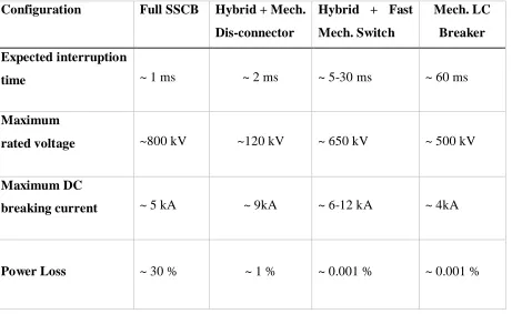
The four configurations were modeled in a Real Time Digital Simulator (RTDS) and the performance of the breakers has been evaluated in a 9 module/2 terminal DC system when a line to ground fault occurs on the DC side. Table 1 summarizes the findings from [3].
Table 1: Summary of Evaluated DC Circuit Breakers.
Configuration Full SSCB Hybrid + Mech.
Dis-connector
Hybrid + Fast
Mech. Switch
Mech. LC
Breaker
Expected interruption
time ~ 1 ms ~ 2 ms ~ 5-30 ms ~ 60 ms
Maximum
rated voltage ~800 kV ~120 kV ~ 650 kV ~ 500 kV
Maximum DC
breaking current ~ 5 kA ~ 9kA ~ 6-12 kA ~ 4kA
6 Another topology of a fast acting DC solid-state fault isolation device for MVDC distribution system was studied in [4]. This paper proposes a Solid State Fault Isolation Device (SSFID) based solution capable of interrupting fault current within 4.042µS from inception of a fault. A micro-controller based approach is adopted to provide such a quick response [4]. Figure 5 shows the Solid State FID topology where micro-controller is the central decision making unit which continuously monitors the current sensor response for an over current condition.
Figure 5: Solid State FID topology [4].
Under steady state condition, the micro controller commands the gate driver to keep the switch in on condition. At the time of fault, the load current rises and its di/dt is limited by using an inductive element. Once a threshold limit is reached, the microcontroller commands the gate driver to turn off the solid-state switch. Diode is required to freewheel the residual current.
Even though this topology is very fast, it still breaks the current at non-zero, and the continuous forward voltage across the high on resistance of the MOSFET will incur high losses of the system.
1.4. Scope
7 winding. The device operates by causing the reverse current in the primary winding when the switch to the pre-charged capacitor is closed. The capacitor is sized such that the current would be sufficient to cause the primary current to fall to zero when the breaker is opened. The detailed operational details and working principle have been explained in Chapter 2.
8
Chapter 2: Proposed DC Circuit Breaker
A novel DC circuit breaker is proposed in this thesis based on the patent [1].
2.1. General description of the Patent
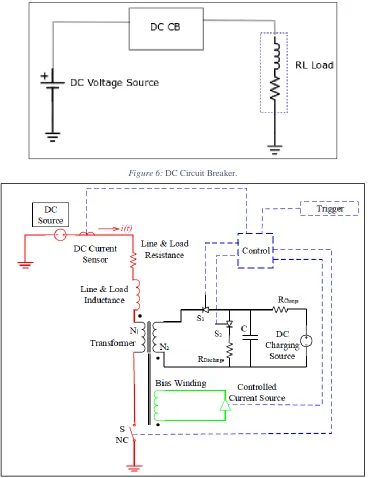
Figure 6 presents the simplified diagram of a DC Circuit Breaker. Like all circuit breakers, it would be connected in series to the load. Figure 7 explains the proposed device connections and topology.
Figure 6: DC Circuit Breaker.
9 Since DC has no natural zero crossing, the presented scheme creates an artificial zero- crossing for current interruption. With the use of an isolating transformer as shown in Figure 7, whose primary winding is connected to the main switch and load, and the secondary winding is connected to a pre-charged capacitor through a switch (S1 in Figure 7). The secondary is connected such that the current through the winding opposes the current through the primary winding. The capacitor is charged using a high-impedance power supply (DC Charging Source in Figure 7).
“The device operates by causing the reverse current in the primary winding when the switch to
the capacitor is closed. The capacitor is sized such that the current is sufficient to cause the
primary current to fall to zero. At this artificially created zero crossing the current in the primary
circuit is interrupted. At the same instant, another switch allows the capacitor to discharge to a
bleeder resistor. This allows the capacitor charge to be maximized without regard to having to
match the device to a particular load.” [1]
“The turns-ratio of the primary to secondary can be used to advantage to reduce the voltage
requirement at the secondary side. In this way, a relatively low capacitor voltage can be utilized
to interrupt a high level of DC voltage. Energy stored in the capacitor must be at least equal to
the energy stored in the magnetic field supported by the DC current plus any saturation energy of the transformer core.” [1]
“A third winding can be introduced into the transformer so that saturation effects can be
eliminated or reduced. The DC current through this winding would be arranged to oppose the
current flow in the primary. This current, typically small, can be dynamically modulated to allow
10
2.1.1. Operational Details
This section explains the initial pre-trip conditions, the trip action and the control circuit logic. Referring to Figure 8, DC Circuit Breaker Circuit Electrical Diagram for physical arrangement and connections.
Figure 8: DC Circuit Breaker electrical diagram.
2.1.2. Initial pre-trip conditions
1. Initially the DC Source provides energy to the load as represented in the Figure 8.
2. The main DC current pathway passes through one winding of an Isolating Transformer. This winding of the transformer should be sized to, carry the full DC current and, withstand the DC voltage of the system. This primary winding has N1 turns. The turn’s ratio of the transformer N1:N2 can be used to advantage to provide an optimal match between capacitor voltage and DC line voltage [1].
11 4. The switch S1 is normally open. It is responsible for current flow from the capacitor to the
transformer winding and then consequently to the primary winding.
5. The switch S2 is normally open, and functions as a discharge switch for the capacitor after the fault is cleared.
6. In the ControlCircuit, the signal indicated in green is the input signal coming from the DC Current Sensor and the ones in blue are output signals to the Breaker, S1, S2 and Controlled Current Source. The threshold current value is preset in the control circuit.
2.1.3. Trip Action
1. In the event of a short circuit, the current in the main branch will drastically rise. The Control Circuit compares the DC Current sensor input to a pre-fed value of short circuit threshold current and the switch S1 is closed. This discharges the electrical energy stored in capacitor across the N2 winding of the transformer. The transformer is connected such that the current that results from the discharge will oppose the main DC current. The result is that when the device is activated the main DC current will be the sum of the normal current and the induced current. The main DC current is be forced to a value below zero. An artificial zero-crossing point is thus generated.
2. At the instant, that the DC Current Sensor indicates to the Control Circuit that the current has been reduced to zero the ControlCircuit directs the main DC switch, Breaker, to open. 3. At the instant that the DC Current Sensor reports to the Control Circuit that the current has
reduced below zero the Control Circuit directs switch S2 to close. This places resistor R2 across the capacitor to dissipate any un-needed energy.
4. The system can be reset to the initial condition by opening switches S1 and S2 and closing switch Breaker.
2.2. Controller Design for the Proposed DCCB
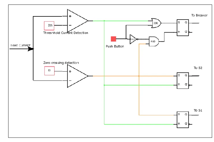
The controller for the proposed DC circuit breaker is designed and implemented as shown in Figure 9. The logic flow of the controller is described below:
1. The current sensor senses the Load Current and sends a signal to the control circuit. 2. This signal is then compared to a threshold value (ith), (set using a potentiometer) using a
12 3. The output of the comparator (green in Figure 9) is true when the Load current exceeds the
threshold value.
4. Another comparator detects the zero crossing and the output of this comparator (in orange in Figure 9) is true when the current goes below zero.
Figure 9: Control Circuit.
5. Output Signal for Breaker should be closed. At zero crossing should be open. 6. The pushbutton is for circuit startup.
7. S-R Flip flops are used to latch the outputs at required instances.
8. Table 2 shows the Control circuit outputs for the short circuit fault event sequence.
Table 2: Control Circuit Output.
Condition Event iload Operations
Breaker S1 S2
1 Normal Operation i >0 & i< ith Closed Open Open
2 Short Circuit
2 a i>0 & i< ith Closed Open Open
2 b i>ith Closed Closed Open
2 c i>0 & i<ith Closed Closed Open
2 d i=0 Open Open Open
13 9. At the event of short circuit condition 2 a from Table 2 when the current rises but is within the specified limit of ith (threshold or pick up current), the switches remain in the same state as the normal operations.
10.At the condition of 2 b when the current crosses the limit of ith, the switch S1 is latched closed (through condition 2c) till current becomes zero, by discharging the capacitor to the transformer winding.
11.At the instance of condition 2 d when current becomes zero, Breaker is latched closed until reset, and S1 is opened to prevent unnecessary capacitor discharge to the main circuit. 12.When current goes below zero at condition 2 e, the switch S2 is closed in order to discharge
the capacitor through the bleeder resistor R2.
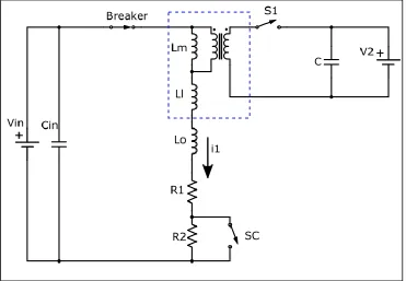
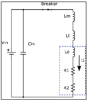
2.3. Theoretical Analysis
Figure 10 shows the DC Circuit Breaker diagram with the Lm and Ll as the magnetizing and leakage inductance of the transformer. Lo, R1 and R2 as the load inductance and resistance, where R2 will be shorted to emulate a short circuit. The breaker switch is in series with the load and Vin is the input Voltage. On the secondary side the capacitor C is charged through V2 Voltage source, and connected to the secondary winding of the transformer through the switch S1.
14 Figure 11 is the timing diagram of the expected current waveform. There are five phases as shown,
• Phase 0 – circuit is disabled and current is zero • Phase I – current rises to steady state value in time t1 • Phase II – steady state operation for time t2
• Phase III – current rising after short circuit • Phase IV – fault clearance
Figure 11: Timing diagram of expected current waveform. Phase I
Figure 12 shows the equivalent circuit diagram and flow of current in the phase I as given in Figure 11. The current rises in the RL circuit and the primary side current can be expressed as given in (1).
𝑖1(𝑡) = 𝑉𝑖𝑛
(𝑅1+𝑅2)(1 − 𝑒
−𝑡
𝜏1) (1)
𝑤ℎ𝑒𝑟𝑒, 𝜏1 =𝐿𝑚 + 𝐿𝑙 + 𝐿𝑜 𝑅1+ 𝑅2
15 Figure 12: Equivalent Circuit Diagram - Phase I.
Phase II
Phase II from Figure 11 shows the steady state and Figure 13 is its equivalent circuit diagram. As the circuit is in steady state condition, only the load resistance is observed and therefore the steady state current can be written as shown in (3).
𝐼𝑠𝑠 = 𝑉𝑖𝑛
𝑅1 + 𝑅2 (3)
Figure 13: Equivalent Circuit Diagram of Phase II. Phase III
16
𝑖1 = 𝐼𝑠𝑠𝑒
−𝑡 𝜏3+𝑉𝑖𝑛
𝑅1 (1 − 𝑒 −𝑡
𝜏3) (4)
𝑤ℎ𝑒𝑟𝑒, 𝜏3 =𝐿𝑚 + 𝐿𝑙 + 𝐿𝑜
𝑅1 (5)
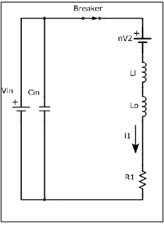
Figure 14: Equivalent Circuit Diagram - Phase III. Phase IV
17 Figure 15: Equivalent Circuit Diagram Phase IV.
Therefore, the current through the circuit is expressed in (6)
𝑖1(𝑡) = 𝐼𝑡𝑟𝑖𝑝𝑒−𝑡𝜏4 −(𝑛𝑉2 − 𝑉𝑖𝑛)
𝑅1
(1 − 𝑒−𝑡𝜏4) (6)
𝑤ℎ𝑒𝑟𝑒, 𝜏4 =𝐿𝑙 + 𝐿𝑜 𝑅1
(7)
𝐴𝑡 𝑡 = 𝑡𝑠𝑐, 𝑖1= 0
0 = 𝐼𝑡𝑟𝑖𝑝𝑒−𝑡𝑠𝑐𝜏4 +(𝑛𝑉2 − 𝑉𝑖𝑛)
𝑅1
𝑒−𝑡𝑠𝑐𝜏4 −(𝑛𝑉2 − 𝑉𝑖𝑛)
𝑅1
(8)
𝑡𝑠𝑐 = 𝜏4 × ln [1 + 𝑅2𝐼𝑡𝑟𝑖𝑝
(𝑛𝑉2 − 𝑉𝑖𝑛)] (9)
18
Chapter 3: Modeling and Simulation
3.1. Circuit Modeling
Based on the working principles explained in Section 2.3, the circuit was modelled on PLECS. Figure 16 shows the PLECS Model of the main circuit, and Figure 17 shows the subsystem model of the control circuit. Table 3 and Table 4 list the circuit specifications for the main circuit and the secondary circuit. The primary purpose of PLECS simulation was to verify the operation of control circuit.
Table 3: Circuit specifications of Main Circuit.
Sno. Specifications Value
1 Voltage 40 V
2 Continuous Current 2 A
3 Load Resistance 20 ohm
4 Load Reactance 1 mH
Table 4: Circuit specifications of secondary circuit.
Sno. Specification Value
1 Voltage 120 V
2 Capacitor 4.7 mF
3 Resistance R1 0.1 ohm
4 Resistance Rcharge 20 ohm
19 Figure 16: DC Circuit Breaker PLECS model.
20
3.2. Results
Figure 7 shows the waveform results of the simulation.
21 At the instant of 0.1 us the signal from the pulse generator gives a high signal acting like a circuit starter to switch the breaker on. Once the current is non zero, the breaker stays latched on to on state and current rises in the circuit to a load current of 2 A.
At the instance of 0.25 ms short circuit is emulated by shorting a resistor. The current in the circuit rises. At the instant of 0.4 ms the threshold of 3 A is crossed and the switch S1 is indicated to close, which enables the current from the capacitor to discharge and oppose the current in the primary side to make it zero at which instant, breaker is opened.
22
Chapter 4: Hardware Design
4.1. Component Selection
Figure 19 shows the Components required for the hardware. The hardware comprises of two parts, • Power circuit - boxed in green in Figure 19, components are listed in Table 5.
• Control circuit - marked in blue in Figure 19, components listed in Table 6.
Figure 19: Proposed hardware design.
4.1.1. Power Circuit
The Power Circuit was aimed to operate at the following maximum operating conditions, • Main DC Voltage = 230 V
23 Table 5:Components of Power Circuit.
*1Two capacitors were connected in series to increase the voltage and such two arrangements were connected in parallel to achieve the 4.7 mF at 1000 V.
4.1.2. Control Circuit
Section 2.2.3 explains the logic implementation of the control circuit. The gate driver listed in Table 4 requires an input signal of 15 V given in datasheet. Therefore, the control circuit was designed for a 15 V output.
Table 6: Components for Control Circuit.
S. No. Component Value Input Voltage Part #
1. Comparator +15, - 15 LM324
2 NAND Gate +15, 0 CD4011B
3 S-R Flip Flops +15, 0 CD4043B
4 Potentiometer +15, - 15 3310
5 Resistor 1.5 k ohm
6 Push button GPTS203211B
S.No. Component Component
Name
Value Voltage
Rating Current Rating Power Rating Component Part#
1. Resistance R(load),
Rcharge
10 ohm 2.5 kW TE 2500 B 10 R
2 Inductance 30 A 195C30
3 Capacitor*1 C 4.7 mF 500 V ALS70A
4 Switches
(IGBT)
Breaker, S1 1200V 114 A SKM75GB12V
5 IGBT Gate
Driver
15V SKHI 61 R
6 Current
Sensor
Current
Sensor
24
4.2. Control Circuit Design
4.2.1. Schematic
The control circuit was designed on EAGLE using the listed components in Table 6. Each components’ footprints were designed referring to the respective datasheets. Figure 20 shows the schematic design and Figure 21 shows the PCB two layer layout.
25
4.2.2. PCB Layout
A two layered Printed circuit board shown in Figure 16 was designed on EAGLE.
Figure 21: PCB layout on EAGLE.
The Printed Circuit Board was soldered with the components listed in Table 5, see Figure 22.
26
Chapter 5: Experimental Results
5.1. Transformer Testing
A four winding transformer with the specifications given in Table 7, were tested to obtain parameters like magnetizing branch inductance and resistance and leakage inductance and resistance.
Table 7: Transformer specification.
S.No. Specification Value
1 Primary Voltage 1 winding 115 V
2 Secondary Voltage 1 winding 115 V
3 kVA rating 1000 VA
4 Rated current 5 A
Figure 23 shows the picture of the transformer used in the hardware setup. It has four windings, two windings in the primary with terminals namely 1 and 2, and 3and 4, the secondary side has two windings with terminals 5 and 6, and 7 and 8. In order to attain a voltage rating of 230 V, terminal 2 and 3 are connected, connecting two windings in series. Similarly, on the secondary side, the terminals 6 and 7 are connected to achieve 230 V.
27 In order determine the parameters of the transformer, Open Circuit and Short Circuit tests were done.
5.1.1. Open Circuit Test
An open Circuit Test was conducted on the transformer at the rated Voltage of 115 V for a single winding on the primary side with a setup shown in Figure 24(a) and with all other windings opened as shown in Figure 24(b). Table 8 shows the results of the open circuit test, using which the magnetizing branch impedance is calculated.
Figure 24: (a) Open Circuit Setup (b) Open Circuit 1 Winding.
Table 8: Open Circuit Results.
Prameter Woc Voc Ioc
Value 190 W 115 V 3.3 A
Using the result of the tests the power factor can be calculated as expressed in (10).
𝑐𝑜𝑠φ = 𝑊𝑜𝑐
𝑉𝑜𝑐 × 𝐼𝑜𝑐= 0.5 (10) φ = 59.95° (11)
Magnetizing component of the no load current (Ioc) is expressed as Im in (12).
𝐼𝑚 = 𝐼𝑜𝑐 𝑠𝑖𝑛φ = 2.856 A (12)
The core component of the no load current (Ioc) is expressed as Ic in (13).
𝐼𝑐 = 𝐼𝑜𝑐 𝑐𝑜𝑠φ = 1.65 A (13)
Therefore, the magnetizing branch reactance Xm can be expressed as in (14).
𝑋𝑚 =𝑉𝑜𝑐
𝐼𝑚 = 40.26 Ω (14)
28
𝑅𝑚 =𝑉𝑜𝑐
𝐼𝑐 = 69.69 Ω (15)
Magnetizing inductance Lm is calculated from (16), where f = 60 Hz.
𝐿𝑚 = 𝑋𝑚
2𝜋𝑓 = 0.106 𝐻 (16)
So, the magnetizing Inductance was calculated as 0.106 H.
5.1.2. Short Circuit test
A short circuit test was conducted on the transformer at rated current of 5 A for two windings on series on both the sides. The short circuit test set up is shown in Figure 25(a) and the two winding connection is shown in Figure 25(b).
Figure 25: (a) Short Circuit Setup (b) Short Circuit two winding.
Table 9: Open Circuit Test Results.
Parameter Wsc Vsc Isc
Value 1.8 W 0.353 V 5.77A
The leakage resistance can be calculated using the results in Table 9 from (17).
𝑅𝑙 =𝑊𝑠𝑐
𝐼𝑠𝑐2 = 0.055 Ω (17) The leakage impedance can be expressed as given in (18), and therefore leakage reactance is calculated in (19).
𝑍𝑙 = 𝑉𝑠𝑐
29
𝑋𝑙 = √𝑍𝑙2− 𝑅𝑙2 = 0.026 Ω (19)
𝑋𝑙 = 2𝜋𝑓𝐿 (20)
Leakage inductance Ll is calculated from (20) where f = 60 Hz.
𝐿𝑙 = 𝑋𝑙
2𝜋𝑓 = 0.07 𝑚𝐻 (21)
The leakage inductance Ll was calculated as 0.07 mH.
5.2. IGBT and Gate driver testing
The gate driver (SEMIKRON SKHI 61 (R)) were tested by giving 15 V input and verifying the output to be the same as the gate pulses at the inputs given using a pulse generator.
The output from the gate drivers were used to check the gate terminals of the IGBT (SEMIKRON SKM75GB12V).
5.3. Transformer Action Test
In order to establish the basic proof on concept regarding the transformer behavior, a simple circuit shown in Figure 26 was tested for the parameters given Table 10. A Capacitor was connected to the secondary through a switch S1 and this switch was closed, by giving a pulse through a pulse generator.
Table 10: Parameters of Transformer Action Test.
Parameter Value
DC Source Voltage 20 V
DC Charging Voltage 60 V
Load Resistance (R) 20 Ω
30 .
Figure 26: Basic Proof of Concept circuit.
Figure 27 shows the waveform of the primary current (yellow) and secondary current (pink). As can be seen the primary current is initially 1 A as the DC Source Voltage is 20 V and resistance is 20 ohms. At in instant, here at -8.4 µs the switch S1 is manually closed, and therefore it can be seen that, secondary current, which is zero initially, starts to increase, indicating flow of current in the secondary circuit and discharging of capacitor. Also with the increase in secondary current, the primary current decreases.
Figure 27: Primary and secondary current waveform.
31 voltage that is 40 V (60-20). This indicates that the secondary side voltage is reflected across the magnetizing inductance at the event when S1 is closed.
Figure 28: Primary Current and Primary transformer Voltage.
Figure 29 shows the voltage across the capacitor and the secondary side circuit’s current. At the instant -8.4 µs when the switch is closed the capacitor discharges allowing the secondary current to flow.
Figure 29: Secondary Current and Capacitor Voltage.
5.4. Control circuit testing
32
5.5. Current Sensor testing
The current sensor LA – 55 P has turns ratio of 1:1000. The voltage of the sensed current was measured across a 470 Ω resistor. Table 10 gives the value of voltage sensed for its respective current. Figure 30 shows the linearity of the relation between the actual current sensed voltages. The current sensor has a calibration of 0.045V/ A.
Table 11: Current Sensor Calibration.
S.No. Actual Current (A) Sensed Voltage (V)
1 0 0.048
2 0.5 0.283
3 1 0.519
4 1.5 0.800
5 2 1.085
6 2.5 1.370
7 3 1.418
8 3.5 1.701
9 4 1.985
Figure 30: Current Sensor Voltage vs Current.
5.6. Measurement instruments and Supplies
For hardware assembly and acquiring results, Table 12 lists the supplies used in the setup and Table 13 lists the oscilloscopes used acquiring the results.
0 0.5 1 1.5 2 2.5
0 1 2 3 4 5
33 Table 12: DC Sources.
S.No. Name Voltage Range
1 TDK Lamba 0-150 V
2 Agilent Technologies DC Power Supply 0-150 V
3 Keysight Triple Output DC Power Supply +25 V , -25 V
Table 13: Oscilloscope.
S.No Oscilloscope
1 Tektronix TDS 2024B
2 Lecroy HDO6104
3 43B Power Analyzer
5.7. Hardware Assembly
All the components were assembled together for testing according to Figure 31. Figure 32 shows the hardware assembly set up.
34 The short Circuit switch is used to short 10 ohm resistor to raise the current in a controlled manner.
Figure 32: Hardware Setup.
5.8. Challenges
This section discusses the problems were encountered while testing the hardware.
5.8.1. Ground Reference for Switches
The switch Breaker and S1 shown in Figure 31 were being given the gate pulses from the same gate driver, and hence were being given the same ground reference, through the same source. This was ultimately shorting the two sides of transformer. In order to debug this problem, another gate driver was used with a separate supply to isolate the gate signal given to the Switches and thus preventing the short.
5.8.2. Current Sensor:
35 offset was 0.022 V, which implied that threshold current and zero reference given through a potentiometer had to include the offset value.
5.9. Short Circuit Protection Test
The setup was tested at 40 V primary Voltage, and the capacitor on the secondary side was charged at 120 V. The load current during pre-trip condition is at 2A. One 10 ohm resistor was shorted using an IGBT switch which was given a pulse using a push button.
Table 14: Circuit Parameters for Short Circuit Protection Test.
Parameter Value
Vin 40 V
V2 120 V
n 1
Ll 0.7 mH
Lo 1 mH
R1 , R2 10Ω
Iss 2 A
36 Figure 33: Circuit Diagram for Short Circuit Protection Test.
5.9.1. Results
37 Figure 34: Primary current.
Figure 35: Primary current and Breaker voltage.
38 Figure 36: Primary current and Secondary current.
As seen in the figures above, there is a lot of noise after the current interruption. This is due to the current breaking at a non zero value. The zero current reference given in the control circuit, through a potentiometer, had to be set to a value greater than the offset of the current sensor, hence inaccurately sensing zero crossing. The delay caused by the current sensor and the control circuit also causes the current to break at a non-zero value.
Figure 37 shows the zoomed in version of current waveform and as can be seen the time to reduce current to zero or the fault clearance time from 3.6 A is 62.76 µs.
39
5.9.2. Verification of Analytical Expression
As derived earlier in Chapter 2 the expression for tsc is,
𝑡𝑠𝑐 = 𝜏4 × ln [1 + 𝑅2𝐼𝑡𝑟𝑖𝑝
(𝑛𝑉2 − 𝑉𝑖𝑛)] (22)
𝑊ℎ𝑒𝑟𝑒, 𝜏4 =𝐿𝑙 + 𝐿𝑜
𝑅2 (23)
𝐿𝑙 = 0.07𝑚𝐻, 𝐿𝑜 = 1𝑚𝐻, 𝑅2 = 10Ω
𝜏4 =(0.07 + 1) × 10
−3
10 = 0.107 𝑚𝑠 (24) 𝑉2 = 120𝑉, 𝑉𝑖𝑛 = 40𝑉, 𝑛 = 1
𝑡𝑠𝑐 = 0.107𝑚𝑠 × ln [1 + 10 × 3.56
(120 − 40)] = 39.38µ𝑠 (25)
40
Chapter 6: Conclusion
6.1. Summary
With the results presented in Chapter 5 the unique concept of the DC Circuit Breaker has thus been proved. The fault clearance time calculated using the analytical expression was in close proximity to the experimental result. Considering the scope of improvement discussed in Section 6.2, the technology can be advanced to make the breaker more reliable, feasible and efficient and can be significantly scaled up for HVDC applications.
6.2. Scope of Improvements
This thesis concentrates on the proof of concept of the patent presented [1]. Section 5.2 discusses the results of the experimental set up of the prototype. The results do present a full proof of the concept but there is scope of improvement, which is discussed in this section.
Firstly, the capacitor size and the DC charging source can be significantly reduced by using the turn ratio of the transformer. By increasing the turns of the secondary side the capacitor size can be reduced to a value which makes the energy on the secondary side (1/2 CV2) greater than the energy on the primary side (1/2 LI2). This can particularly be used for High Voltage Direct Current (HVDC) applications where the turn ratio could bring down the voltage on the secondary side significantly.
Secondly, as mentioned in [1] a third winding can be introduced into the transformer so that saturation effects can be eliminated or reduced. The DC current through this winding would be arranged to oppose the current flow in the primary. This current, typically small, can be dynamically modulated to allow reduction of saturation effects over a wide range of primary current values.
41
REFERENCES
[1] Leonard White, Subhashish Bhattacharya, “16-017 DC Circuit Breaker”, December 2016
[2] S. J. K. Berg, “Solid state circuit breakers in mvdc systems," December 2017.
[3] M. Mobarrez, M. G. Kashani, S. Bhattacharya and R. Adapa, "Comparative study of DC circuit breakers using realtime simulations," IECON 2014 - 40th Annual Conference of the IEEE Industrial Electronics Society, Dallas, TX, 2014, pp. 3736-3742
[4] S. Juvekar, B. Compton and S. Bhattacharya, "A fast acting DC solid state fault isolation device (FID) with Si and SiC devices for MVDC distribution system," 2012 IEEE Energy Conversion Congress and Exposition (ECCE), Raleigh, NC, 2012, pp. 2005-2010.
[5]Christoph Meyer, Maurice Kowal, Rik W. De Doncker,” Circuit Breaker Concepts for Future High-Power DC-Applications”, Institute for Power Electronics and Electrical Drives RWTH Aachen University
[6] B. Pauli et al., “Development of a high current HVDC circuit breaker with fast fault clearing capability,” IEEE Trans. Power Del., vol. 3, no. 4, pp. 2072–2080, Oct. 1988.
[7] C. Meyer and R. W. De Doncker, “Solid-state circuit breaker based on active thyristor topologies,” IEEE Trans. Power Electron., Mar. 2006.
[8] Z. John Shen, Zhenyu Miao, and Aref Moradkhani Roshandeh,” Solid State Circuit Breakers for DC Micrgrids: Current Status and Future Trends”
[9] C. Meyer, M. Kowal, and R. W. De Doncker, “Circuit breaker concepts for future high- power DC-applications,” in 40th Conf. Rec.IEEE IAS Annu. Meeting, Hong Kong, Oct. 2005, pp. 860–866.
[10] Ataollah Mokhberdoran*, Adriano Carvalho, Helder Leite, Nuno Silva,” A Review on HVDC Circuit Breakers”, Department of Electrical and Computer Engineering, University of
Porto, Portugal
![Figure 5: Solid State FID topology [4].](https://thumb-us.123doks.com/thumbv2/123dok_us/1185238.1148925/17.612.147.468.215.417/figure-solid-state-fid-topology.webp)