ABSTRACT
CARLIN, CONRAD ZACHARY. MOCVD Growth and Modeling of Quantum-well Solar Cells and Tunnel Junctions. (Under the direction of Dr. Salah M. Bedair).
One source of photovoltaic energy is the multijunction (MJ) solar cell, which has given the highest
efficiencies of any photovoltaic technology. Typical MJ devices are composed of several pn junctions
with materials of differing band gaps. Ideally, each material is lattice matched and current match to
each other, requiring the proper choice of semiconductor for each junction. The limited availability of
semiconductors with these characteristics has in the past required the either the lattice matching or
current matching be violated, reducing the maximum potential efficiency. For terrestrial applications,
multijunction structure are cost efficient only when operated at high solar concentrations. One of the
main limits to the solar concentration is the maximum current that can be supported by the tunnel
junctions (TJ) between multijunction subcells.
Solar cells were grown by metal organic chemical vapor deposition based on a GaAs p-i-n structure
with an i-layer containing low band gap InGaAs is grown as thin, compressively strained layers that
are compensated with GaAsP layers under tensile strain. The resulting structure is lattice matched to
the GaAs substrate and the InGaAs quantum wells (QW) absorb at a lower energy than the GaAs,
lowering the effective band gap of the subcell. The bandgap of InGaAs wells were modeled using a
modified Kronig-Penney model to include the effects of strain and quantum confinement. However,
device external quantum efficiency (EQE) measurements showed that the actual QW absorption
energy edge was higher than expected. It was found that this behavior could be modeled as a graded
interface between the InGaAs and GaAsP layers. The effect of this grading was found to be strongest
for the interface formed during the transition from GaAsP to InGaAs and the effects could be
minimized by including a layer of GaAs between the two materials.
Each QW structure used GaAs1-yPy with high phosphorus compositions (x>0.65), requiring transport
to occur through tunneling. For this reason reductions in EQE were observed for barriers thicker than
30 Å. These thick barrier devices were useful for investigating the transport through the QW
structures. EQE measurement of p-i-n and n-i-p QW structures indicate that carrier transport through
the i-layer was limited by electrons. An empirical model was developed to calculate the EQE of both
GaAs pn and QW p-i-n devices. Both the tunneling and probability and lifetime were determined,
making it possible to find the recombination lifetime in the wells. This was found to be 110 ns for
For a Ge/GaAs/InGaP MJ cell the critical TJ is between the GaAs and InGaP subcells must have a
band gap above 1.9 eV to avoid parasitic absorption. It was found that the performance of the n++
-InGaP/p++-AlGaAs TJ was greatly improved by growing a thin (<50 Å) GaAs layer at the InGaP-AlGaAs interface, with the peak tunneling current (Jpk) increasing from 18 A/cm2 to >1000 A/cm2.
The tunneling current has an exponential dependence on the tunneling width and effective mass, so it
is very sensitive to doping and material composition near the junction. Neither direct tunneling nor
trap assisted tunneling models could adequately explain the observed Jpk. However, the high Jpk can
be explained by either the carryover of In into the GaAs to form InGaAs or by the formation of a
highly doped layer at the InGaP-GaAs interface. The success of these models can be explained by the
reduction of the tunneling width due to the presence of GaAs (or InGaAs) QW within the tunneling
© Copyright 2015 Conrad Zachary Carlin
MOCVD Growth and Modeling of Quantum-well Solar Cells and Tunnel Junctions
by
Conrad Zachary Carlin
A dissertation submitted to the Graduate Faculty of North Carolina State University
in partial fulfillment of the requirements for the degree of
Doctor of Philosophy
Electrical Engineering
Raleigh, North Carolina
2015
APPROVED BY:
_______________________________ _______________________________
Salah. M. Bedair Nadia El-Masry
Committee Chair
_______________________________ _______________________________
ii
BIOGRAPHY
Conrad Zachary Carlin was born on October 30, 1981 in Raleigh, North Carolina. His father, Clifford
Million Carlin, Jr. and his mother, Lisa Johnston Carlin are both graduates of North Carolina State
University with a Ph.D. in chemistry and an M.S in biology, respectively. After the completion of his
father’s degree, he lived in Austin, Texas; Orono, Maine and Charlotte, North Carolina. He graduated
from Harding University High School in 2000 and from the University of North Carolina at Charlotte
in 2005 with a B.S. in chemistry. His interests include reading, classical music and Carolina Panthers
iii
ACKNOWLEDGMENTS
The author would like to thank his family for their support and Dr. John Hauser for his assistance
iv
TABLE OF CONTENTS
LIST OF TABLES ... viii
LIST OF FIGURES ... ix
1. Comparison of energy sources ... 1
1.1. Criteria for evaluating energy sources ... 2
1.2. Current energy sources ... 4
1.3. Future energy sources ... 6
1.4. The potential for photovoltaics ... 7
2. Basics of photovoltaics ... 9
2.1. Solar irradiance and the solar spectrum ... 9
2.2. Band structure and light absorption ... 10
Origin of band structure ... 10
2.2.1. Charge carriers ... 12
2.2.2. Generation and recombination... 14
2.2.3. 2.3. Fundamentals of pn junctions ... 16
Diode equation... 16
2.3.1. Diode equation for photovoltaics ... 17
2.3.2. 2.4. Photovoltaic principles ... 18
Short circuit current ... 18
2.4.1. Open circuit voltage ... 18
2.4.2. Fill factor ... 19
2.4.3. Quantum efficiency ... 19
2.4.4. Efficiency ... 19
2.4.5. Sources of loss and maximum efficiency ... 20
2.4.6. 2.5. Components of photovoltaic devices ... 20
Emitter and Base ... 21
2.5.1. Window ... 21
2.5.2. Back surface field ... 21
2.5.3. Metal contacts ... 22
2.5.4. 3. Multijunction photovoltaics, Quantum wells and superlattices, and tunnel junctions ... 23
3.1. Multijunction photovoltaics ... 23
Advantages and disadvantages of multijunction photovoltaics ... 23
3.1.1. Types of multijunction structures ... 26
v
3.2. Quantum wells and superlattices ... 29
Formation of quantum wells and superlattices ... 30
3.2.1. Quantum size effect ... 31
3.2.2. Strained quantum wells and strain balanced superlattices and their application to 3.2.3. multijunction solar cells ... 32
3.3. Tunnel junctions ... 34
Origin of the tunnel junction ... 34
3.3.1. Use of tunnel junctions in multijunction structures ... 36
3.3.2. 4. MOCVD and device and material characterization ... 37
4.1. Metal organic chemical vapor deposition ... 37
Components of MOCVD system ... 38
4.1.1. 4.1.1.1. Bubblers and gas sources ... 38
4.1.1.2. Vent/run manifold ... 39
4.1.1.3. Reactor ... 40
4.1.1.4. Exhaust system ... 41
Substrate preparation ... 41
4.1.2. MOCVD growth ... 42
4.1.3. 4.1.3.1. Purge and bake out ... 42
4.1.3.2. Nucleation ... 42
4.1.3.3. Growth ... 43
4.2. Device and material characterization ... 44
Hall effect characterization ... 44
4.2.1. X-ray diffraction ... 45
4.2.2. Photoluminescence ... 46
4.2.3. Light JV response ... 46
4.2.4. External quantum efficiency ... 46
4.2.5. 5. Quantum well structures: Modeling and experiment ... 48
5.1. Modeling of quantum well states ... 48
Kronig-Penny model for superlattices ... 48
5.1.1. Effect of strain on energy states in quantum wells ... 52
5.1.2. Modified Kronig-Penny model for non-abrupt interfaces ... 55
5.1.3. Effect of built-in electric field on energy states in quantum wells ... 61
5.1.4. Constraints for quantum well structures: strain-balancing and carrier transport ... 62
5.1.5. 5.1.5.1. Critical layer thickness ... 62
vi
5.1.5.3. Carrier transport ... 64
Optimization of composition and thickness of strain-balanced quantum wells and 5.1.6.
barriers 65
5.2. Extension of absorption in quantum well solar cell devices... 67
The p-GaAs/i-MQW/n-GaAs solar cell structure ... 68 5.2.1.
The effect of quantum well composition and thickness on absorption extension ... 69 5.2.2.
The addition of GaAs layers at InGaAs/GaAsP interfaces and the effect on interface 5.2.3.
grading 72
6. Effect of barrier width on carrier transport ... 76 6.1. Effect of barrier thickness on EQE ... 76
Effect of device polarity: importance of electron transport ... 76 6.1.1.
Effect of temperature and bias on EQE ... 79 6.1.2.
6.2. Empirical model for EQE of solar cell devices. ... 80
EQE for p-n GaAs structures ... 80 6.2.1.
Calculation of absorption in MQW structures ... 83 6.2.2.
6.2.2.1. Single-carrier absorption ... 83
6.2.2.2. Excitonic absorption ... 84
EQE of MQW solar cell structures ... 84 6.2.3.
Determination of recombination lifetime from EQE modeling ... 85 6.2.4.
7. InGaP/GaAs/AlGaAs tunnel junctions ... 90 7.1. Growth of highly doped materials ... 90
Te doping in InGaP ... 90 7.1.1.
Te doping in GaAs ... 91 7.1.2.
C doping in AlGaAs ... 92 7.1.3.
7.2. InGaP/AlGaAs tunnel junctions ... 93
7.3. The addition of a GaAs interfacial layer to InGaP/AlGaAs tunnel junctions ... 94
The effect of GaAs thickness... 95 7.3.1.
Annealing of InGaP/GaAs/AlGaAs tunnel junctions ... 96 7.3.2.
7.4. Modeling of tunneling current ... 96
Kane model ... 97 7.4.1.
Transfer matrix model ... 99 7.4.2.
7.4.2.1. Direct tunneling ... 99
7.4.2.2. Resonant trap assisted tunneling ... 100
Thermal diffusion of dopants and diffusion barriers ... 102 7.4.3.
vii
Indium carryover from InGaP into GaAs ... 112 7.4.5.
viii
LIST OF TABLES
Table 3.1: The ideal band gaps and maximum efficiency for 1, 2 and 3 junction PV cells at one sun and infinite sun concentration of the AM1.5D spectrum. ...26
Table 4.1: Summary of metalorganic precursors used in this work. ...39
Table 6.1: Calculated tunneling lifetime, transmission probability and recombination lifetime for
various device polarities and GaAsP barrier thicknesses. ...87
Table 7.1: Efficiency loss from absorption from GaAs in top tunnel junctions.. ...94
Table 7.2: Comparison between measured and calculated Jpk for various GaAs thicknesses using a
ix
LIST OF FIGURES
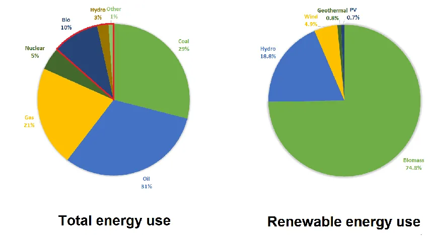
Figure 1.1: Distribution of total energy use and renewable energy use by source. The red line highlights renewable energy sources. Photovoltaic and solar thermal energy generation are currently a small portion of both renewable energy use and total
energy use. ... 1
Figure 2.1: Spectral irradiance for the AM0, AM1.5G and AM1.5D standard solar spectra as
defined by ASTM. ... 10
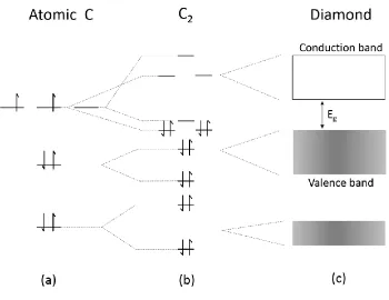
Figure 2.2: Formation of the band structure. The (a) atomic electronic states for a carbon atom form (b) molecular states for the diatomic carbon and the number of quantum states is preserved. The transition from discrete molecules to the (c) periodic diamond
structure results in the formation of bands rather than discrete molecular states. ... 11
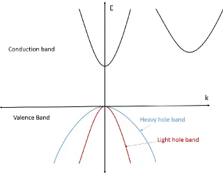
Figure 2.3: Simplified band structure for a semiconductor. The valence band minimum is always at k=0 and for unstrained materials is composed of two degenerate bands, the light hole band and the heavy hole band. The conduction band minimum is shown to be at k=0, but it may be at k≠0 for other semiconductors. ... 13
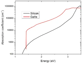
Figure 2.4: Absorption coefficient of silicon and gallium arsenide as a function of photon energy. Since the GaAs is a direct band gap semiconductor, it has a much larger absorption coefficient at most energies. ... 15
Figure 2.5: Valence and conduction band structure for a typical pn junction. ... 16
Figure 2.6: J-V response of a photovoltaic cell in the dark (dark current) and under illumination (light current). ... 18
Figure 3.1: Three possible configurations for incorperating semiconductors of different band gaps into a photovoltaic system: (a) a heterojunction diode with different n-type and p-type materials (b) spatial separation of incoming radiation onto PV cells with different band gaps (c) a multijunction tandem cell with subcells connected
materially, optically and electrically in series. ... 24
Figure 3.2: Plot of band gap versus lattice constant for several III-V semiconductors. The connecting lines represent ternary alloys with black lines for direct semiconductors and red for indirect semiconductors. The two vertical blue lines correspond to materials lattice matched to the common GaAs/Ge and InP substrates The
composition dependent band gaps and lattice constants were found from [7]. ... 25
Figure 3.3: Schematic of the lattice matched, metamorphic and inverted metamorphic triple
junciton PV cells showing typical band gaps for each of the three subcells. ... 27
Figure 3.4: Physical layout of three reduced dimension semiconductor structures: the quntum well, the quantum wire and the quantum dot. The superlattice is formed from a series of closely spaced quantum wells. ... 30
Figure 3.5: Demonstration of the quantum size effect in three In0.15Ga0.85As quantum wells. The
confined states for electrons and heavy holes are shown for each well, light hole states are omitted for simplicity. Thinner wells show more severe quantum size
effects. ... 32
x
The distortion in the lattice constant for the strained layers in the plane of the
substrate results in an opposite distortion in the perpendicular dimension. ... 33
Figure 3.7: Tunnel diode mechanism: a) Degenerate doping in both the n and p sides creates a path for tunneling at low bias, b) as the bias increases direct tunneling becomes impossible and the current decreases to a minumum value and c) at a suffiently large bias the junction behaves like a typical diode. ... 35
Figure 4.1: Functional schematic of the Thomas Swan reactor... 37
Figure 4.2: Photograph of the growth chamber attached to the MOCVD system.. ... 40
Figure 4.3: Schematics for the GaAs-SLS photovoltaic cell and the InGaP/AlGaAs tunnel
junction. ... 44
Figure 5.1: Wavefunction of the lowest energy state of an electron in a a) quantum well and b) superlattice 49
Figure 5.2: E-q dispersion of a 100 Å In0.15Ga0.85As/ 30 Å GaAs0.25P0.75 superlattice (red) with the
energy states of an equivalent isolated quantum well (black)... 51
Figure 5.3: Schematic showing the effect of compressive and tensile strain on the band structure around k=0 ... 53
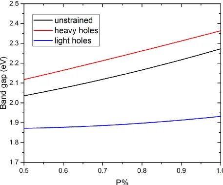
Figure 5.4: Effect of strain on the band gap of InxGa1-xAs for x<0.5 ... 54
Figure 5.5: Effect of strain on the band gap of GaAs1-yPy for y>0.5. The minimum band gap is the
X band of the conduction band for all compositions within the given range. ... 55
Figure 5.6: Calculated effective band gap for InxGa1-xAs/GaAs0.15P0.85 superlattices showing
larger effective band gaps as found from EQE measurements of p-i-n SLS devices. ... 56
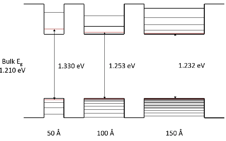
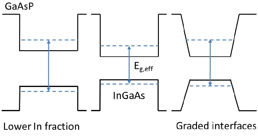
Figure 5.7: Potential sources of effective band gap increase in superlattice structures. There are two modifications of the center well that could give a larger effective band gap: a lower indium fraction (left) and grading the in the P or In composition at interfaces (right). ... 57
Figure 5.8: Schematic of the conduction band envelope function for superlattices with a) abrupt and b) graded interfaces. ... 59
Figure 5.9: Effective band gap for InxGa1-xAs/GaAs0.15P0.85 superlattices with and without grading
at the InGaAs/GaAsP hertrointerface. ... 61
Figure 5.10: Critical layer thickness for InGaAs and GaAsP on GaAs calculated using the model of Matthews and Blakeslee. ... 63
Figure 5.11: Effective band gap for an abrupt interface InGaAs/GaAsP SLS. The purple line is the CLT constraint for InGaAs and the solid orange line is the CLT constraint for GaAsP. The dotted orange lines are the 30 Å barrier thickness tunneling constraint for GaAs1-yPy ranging from y=0.65 to y=0.85. ... 66
Figure 5.12: Effective band gap for a 20 Å graded interface InGaAs/GaAsP SLS. The purple line is the CLT constraint for InGaAs and the solid orange line is the CLT constraint for GaAsP. The dotted orange lines are the 30 Å barrier thickness tunneling constraint for GaAs1-yPy ranging from y=0.65 to y=0.85. ... 67
xi
Figure 5.14: EQE showing the extension of absorption due to In0.17Ga0.83As and In0.23Ga077As
wells with 25Å GaAs0.25P0.75 barriers. ... 71
Figure 5.15: EQE showing the extension of absorption due to In0.18Ga0.83As and In0.15Ga0.77As wells with 30Å GaAs0.22P0.78 barriers. ... 72
Figure 5.16: PL response of superlattice showing the effect of increasing the GaAs thickness as both ternary/ternary interfaces. ... 74
Figure 5.17: EQE of In0.18Ga0.82As/GaAs0.35P0.65 superlattice devices with 25, 50 and 75 Å GaAs buffer layers at the P→In interface. ... 75
Figure 6.1: J-V response for three solar cell devices: 1. A GaAs standard cell, 2. a device with an In0.18Ga0.82As/GaAs0.21P0.79 superlattice and 30 Å barrier and 3. the same superlattice with 34 Å barriers. ... 77
Figure 6.2: Standard, thin barrier and thick barrier solar cell devices with a) n on p polarity and In0.18Ga0.82As/GaAs0.21P0.79 superlattices and b) p on n polarity and In0.15Ga0.85As/GaAs0.20P0.80 superlattices. ... 78
Figure 6.3: EQE of n on p thick barrier superlattice devices as a function of (a) device temperature and (b) reverse bias. Both higher temperatures and larger reverse bias increase the EQE above 600 nm due to an improvement in carrier transport. ... 80
Figure 6.4: Experimental and modeled EQE for a GaAs with a) an n on p polarity and b) a p on n polarity. Also shown are the contributions to the EQE from the emitter, base and depletion region. ... 85
Figure 6.5: The modeled and measured EQE for thick barrier devices with a) an n on p polarity and b) a p on n polarity. The EQE contributions from the base, emitter and SLS layers are included. Ptot was adjusted to give the best fit to the measured EQE. ... 87
Figure 6.6: Modeled and measured EQEs for the n on p thick barrier device at several temperatures. The value of Ptot increases with increasing temperature and is near 1 at 107 °C. ... 89
Figure 7.1: Hall n-type doping versus DETe flow for GaAs ... 91
Figure 7.2: Hall p-type doping and growth rate versus CBr4 flow for AlGaAs ... 92
Figure 7.3: J-V response of an InGaP/AlGaAs tunnel diode ... 94
Figure 7.4: Peak tunneling current for an n-InGaP/n-GaAs/p-AlGaAs TJ for several GaAs thicknesses ... 95
Figure 7.5: InGaP/GaAs/InGaP with the quantum well model for a single trap state ... 101
Figure 7.6: Modeled J-V response for a TJ with direct tunneling and TAT for traps with densities of 1015 cm-3 and 1019 cm-3 ... 102
Figure 7.7: Peak current for an annealed InGaP/AlAs/AlGaAs TJ as a function of the AlAs diffusion barrier thickness... 104
Figure 7.8: Peak current density as a function of InGaP thickness for annealed InGaP/AlGaAs tunnel junctions ... 105
Figure 7.9: Peak current density versus spike doping for various thicknesses of the spike layer in InGaP ... 106
xii
Figure 7.11: Peak current density versus spike doping for various GaAs thicknesses ... 108
Figure 7.12: Peak current density versus spike doping for various doping levels in GaAs ... 109
Figure 7.13: Peak current density versus GaAs doping for various GaAs thicknesses and a
4.8×1019 cm-3 InGaP doping spike. ... 110 Figure 7.14: Band profile for InGaP/GaAs/AlGaAs TJ with low (2.2 x 1018 cm-3) and high (2.2 x
1019 cm-3) doping in GaAs ... 111 Figure 7.15: Donor doping profile before and after annealing at 650 °C for 30 minutes ... 112
Figure 7.16: Peak tunneling current versus GaAs for annealed and unannealed TJ with (a) 30 Å doping spike and (b) thick InGaP layers ... 112
Figure 7.17: Peak tunneling current density versus indium composition for an
InGaP/InGaAs/AlGaAs TJ for a 15, 30, and 45 Å InGaAs thickness. ... 114
Figure 7.18: Peak tunneling current versus indium composition for an InGaP/GaAs/AlGaAs TJ with 30 Å GaAs. The indium carryover is modeled as a constant composition region at the InGaP/GaAs interface. ... 115
Figure 7.19: Peak tunneling current versus indium composition for an InGaP/GaAs/AlGaAs TJ with 45 Å GaAs. The indium carryover is modeled as a constant composition region at the InGaP/GaAs interface. ... 116
Figure 7.20: Peak tunneling current density versus doping density in the GaAs of a
InGaP/GaAs/AlGaAs TJ with a 10 Å In0.4Ga0.6As layer representing the indium
1
1.
Comparison of energy sources
Energy is essential for the existence of modern, industrial civilization. The gross domestic product
(GDP) per capita is strongly correlated with the energy use per capita in a country [1]. The growth of
a modern economy requires the development of energy resources and must be constantly evaluated if
this growth is to continue. The ideal source of energy is plentiful, cheap, reliable, safe, and has a
minimal impact on the environment, but there is no single source of energy that fulfills all of these
requirements at any particular place and time. This has led to the development of several different
energy sources and different methods to harness each of these resources. One particularly large
energy resource is the Sun. The total yearly energy transmitted from the Sun to the Earth as radiation
is 5.46×10¹⁸ MJ [2], which is ten thousand times the current world energy use per year. All of the
currently exploited energy sources, except for nuclear and geothermal energy, are ultimately the
product of solar energy. However, it is also possible to produce electrical energy directly from this
solar radiation as photovoltaic energy. To properly evaluate the potential of photovoltaic energy
generation, it is necessary to compare it both to current and emerging energy sources.
Figure 1.1: Distribution of total energy use and renewable energy use by source. The red line highlights renewable energy sources. Photovoltaic and solar thermal energy generation are currently a small portion of both renewable
2
1.1.Criteria for evaluating energy sources
Worldwide energy usage totaled 5.61×10¹⁴ MJ in 2012, the breakdown of which into different sources is shown in figure 1 [1]. The majority of energy production is from coal, oil and natural gas,
which are collectively known as fossil fuels since they are produced from the decomposition of
marine and terrestrial lifeforms over time periods on the order of millions of years. The primary
drawback of fossil fuels is that they are non-renewable, which means that they will be depleted well
before they have the chance to regenerate. The other three major sources of energy are nuclear,
hydroelectric and biomass. Nuclear fission is a non-renewable energy source that is subject to the
depletion of uranium and thorium reserves. Hydroelectric and biomass are renewable sources of
energy but they have a limited capacity for growth since efficient generation of hydroelectric energy
requires large, swift moving rivers, many of which are already in use [3] and biomass is inefficient in
terms of land use and competes with the growth of food sources [4]. To maintain the current rate of
energy usage will require the development of other renewable sources of energy.
This chapter will briefly summarize the advantages and disadvantages of various energy resources
that are either in use or are in development for use in the near future. Since solar energy is currently
an underutilized resource, it will conclude with an evaluation of the role photovoltaics have in as a
future energy source in comparison to current and developing resources.
There are several criteria for evaluating an energy resource. Some of these criteria will be more
important for particular resources.
1. Cost: Cost is probably the single most important consideration when evaluating the potential
for a particular resource [5]. The low cost of fossil fuel sources is responsible for their
dominance as the primary energy sources on the planet. The success of any energy source
depends upon being able to compete with coal as a source of electricity and oil as a
transportation fuel. Technological development of alternative energy sources has often come
when the cost of existing energy sources was high [6].
2. Current and potential reserves: One way to categorize energy resources is either as
renewable or non-renewable. A renewable resource is one where the rate of usage is lower
than the rate of replenishment. This means that the renewable/non-renewable distinction can
depend upon how fast it is being utilized. For instance, wood is considered a renewable
energy source, but forests can take decades to replenish [7]. This has led to the depletion of
3
3. Environmental impact: Most energy resources have some environmental impact, although it
varies depending upon the source. The burning of fossil fuels releases sulfur dioxide (SO2),
nitrogen oxides (NOx) and carbon dioxide (CO2) as waste products. SO2 and NO2 are known
to produce acid rain [9] and CO2 is a greenhouse gas and has been shown to be responsible
for an increase in global temperatures [10]. The cost of many environmental effects of energy
generation are not borne by either the producers of the consumers of energy resources. These
effects can be mitigated by requiring energy producers to include technological solutions to
minimize the environmental impact of energy generation or to impose fines or issue tradable
pollution credits [11] so that the environmental impacts are included in the cost of that
particular energy resource.
4. Reliability: The demand for energy is not constant over the course of a day or a year. For
instance, electrical demand is often higher during the day than the night. Colder climates will
require more energy for heating during the winter while in warmer climates more energy is
required in the summer for air conditioning. The minimum energy demand is called the base
load while the maximum energy demand is the peak load. Periodic energy sources that do not
correlate to the demand cycles must include other sources that can be supplied continuously
and can be increased in response to increases in demand.
5. Scalability: Some energy sources, such as hydroelectric and geothermal, can be produced
more efficiently in particular locations. This leads to the situation where the regions with the
lowest cost of generation can be fully exploited, limiting further growth of a particular
resource. There is also some concern with the scalability for developing energy resources.
Many of the most efficient methods of photovoltaic energy generation use rare elements such
as indium and tellurium. The availability of these materials may limit the ability of these
technologies to be used for large-scale electrical generation [12].
6. Political and social impacts: Energy resources are rarely located in the same place that they
are utilized. This often results in trade between energy rich producer countries and energy
poor consumer countries. The Organization of Petroleum Exporting Countries (OPEC) was
founded in 1960 to serve the interests of the largest oil exporting nations [13]. Wars and
social unrest in these countries has resulted in periods with high oil prices. This has
encouraged the development of energy resources that are not as vulnerable to supply
4
1.2.Current energy sources
These are resources that are currently responsible for the majority of mankind’s energy use. As of
2012 they represent 99% of all energy use.
1. Coal
Coal is formed from terrestrial plant matter than has transformed over long periods of time to a
material that is comprised primarily of carbon with impurities of hydrogen, oxygen, nitrogen and
sulfur. It is the second most important energy source behind oil and is the largest source for
electricity generation, with 40% of electricity worldwide produced from coal [4]. While
hydroelectric and geothermal resources are the lowest cost sources when available, they are
geographically limited to certain locations, which often makes coal the cheapest option for
electrical generation. Given the current demand for coal, there are enough proven reserves to last
more than one hundred years [14]. The primary drawback of coal is that it is a significant source
of particulates, SO2 and CO2. Particulates and SO2 can be removed from the exhaust of power
plants with a small increase in electrical prices [15]. To date there is no economically feasible
method for removing CO2, making coal one of the primary sources of greenhouse gases.
2. Oil
Oil, or petroleum, is formed from the decomposition of marine organisms. It is composed of a
mixture of hydrocarbons with five or more carbon atoms; lighter hydrocarbons are known as
natural gas. Crude oil is almost always processed by distillation, which roughly separates its
components by molecular weight. Petroleum distillates are primarily used as transportation fuels
due to their high energy density [16], but they are also used as a feedstock for the chemical
industry and in the construction of asphalt roadways. It is used less often as a source of electrical
generation due to higher costs, but the ability to quickly increase the power from oil burning
generators make it useful for periods of peak demand. Oil suffers from many of the same
environmental issues as coal as it releases SO2, NOx and CO2 as exhaust products. The remaining
reserves of crude oil are less than those of coal, with 35 more years of proven reserves remaining
[14].
3. Natural gas
Natural gas is composed of lighter hydrocarbons with between one and four carbon atoms per
molecule. It is often found in the same location as crude oil, but also exists as separate gas only
deposits. In the past it was often burnt off or otherwise discarded during the extraction of crude
oil due to technological difficulties with extraction and transportation, but is now the third largest
source of energy behind coal and oil. It does have some environmental benefits relative to the
5
the only exhaust products are carbon dioxide and water. Also, natural gas produces a larger
amount of energy per mole of carbon dioxide released in comparison to coal and petroleum
distillates [17]. Current reserves are expected to last 37 years [14].
4. Nuclear fission
Certain isotopes of very heavy elements such as thorium, uranium and plutonium can release
large amounts of energy when bombarded with neutrons. The energy released is much larger than
from fossil fuels. For instance unenriched uranium can release 500 GJ of energy per kilogram of
fuel compared to coal which will release only 25 MJ when one kilogram is burned [18]. Currently
nuclear fission is responsible for 4.8% of the energy produced in the world, but it is a major
source of electricity in some countries; in France nuclear power is responsible for 73% of all
electrical generation [19]. The main drawbacks of nuclear power are the production radioactive
waste and the potential for nuclear accidents that can render large areas uninhabitable. The major
accidents at Chernobyl in 1986 and Fukushima in 2011 have resulted in a decrease in the
construction of new nuclear plants and some countries have even abandoned nuclear power
altogether. Despite this, nuclear is promising as it is one of the few mature energy technologies
that does not produce any greenhouse gases. Current reserves are capable of providing energy for
78 years [20]. Breeder reactors, which are capable of transmuting non-fissile isotopes into fissile
ones could extend the life of nuclear fuels indefinitely [21].
5. Hydroelectric
Hydroelectric generation uses the potential energy in a flowing river to power electrical turbines.
Large hydroelectric plants often involve the construction of a dam on a river in order to provide
more control over generation. Currently hydroelectric is responsible for 2.4% of the energy
produced in the world. It is a renewable resource and produces no greenhouse gases, but does
have some downsides. Hydroelectric plants must be built on rivers that have high volumetric
flows and large changes in elevations, which limits their geographic distribution. The
hydroelectric potential of the world’s rivers is about 13.5 PWh of which 2.77 PWh, or 21%, is
currently in use [22].
6. Biomass
The burning of wood, peat and agricultural waste was the primary energy source for most of
pre-industrial civilization and is still a major source of energy in many economically undeveloped
nations. Biomass also includes the more technologically advanced biofuels, which are products
such as methanol, ethanol and methane that are produced from the decomposition or fermentation
6
be renewable but it can also be non-renewable if it is being exploited faster than it can be
replenished. When used renewably it is produces no net CO2 since any CO2 produced during
burning is recaptured by growing plant material. One drawback of biomass is that it is very
inefficient in terms of land and water use. Once hectare of land produces 72 GJ of biomass energy
as ethanol from corn, which would require 77 million hectares, or half of the earth’s land area, to
supply all current energy use [23].
1.3.Future energy sources
These energy sources currently represent about 1% of the total energy production of the world. Some,
such as wind and solar photovoltaic, have been successfully implemented but require further
technological development in order to be competitive with other energy sources. All of these sources
are renewable or, in the case of nuclear fusion, use a fuel that is practically inexhaustible.
1. Wind
Wind is the result of pressure differences caused by unequal heating by the Sun on the Earth’s
surface. The total amount of energy available from wind has been estimated to be 2.3 × 10¹⁵ MJ, greater than the total world energy use [24]. As with other sources of energy from natural
phenomena, some locations, such as mountain and coastal areas, are more conducive to wind
generation. These locations have the advantage having little other economic use, but their
remoteness makes it difficult to integrate wind generators into the existing electrical
infrastructure.
2. Nuclear fusion
Nuclear fusion is the generation of energy by combining small nuclei into larger ones. It has the
capability to provide energy even more efficiently than nuclear fission. Furthermore, the best
fission candidates are the isotopes of hydrogen deuterium and tritium, which can be produced
from seawater and lithium, respectively. This means that fusion has the potential provide power
for more than 23 million years and indefinitely if other fusion reactions were to be exploited [25].
However, fusion reactions require very high temperatures (> 106 K) which precludes the use of
any material to contain the reaction. Currently all containment methods require more energy than
what can be extracted from the fusion reaction.
3. Tidal, wave and ocean current
All of these methods are similar to hydroelectric in that they harness the power of moving water.
Tidal uses the change in elevation in the water due to the tides to produce energy. The average
displacement between low and high tide is only 4 m, but this can be amplified by the geography
7
harness the energy of water far from the shore, which creates engineering challenges in installing
and maintaining generating systems and transmitting energy from so far offshore.
4. Geothermal
There is a large amount of thermal energy stored in the earth’s core and mantle. In some locations there are hot regions close enough to the earth’s surface so that either hot water or steam can be
extracted in order to power electrical turbines. Like hydroelectric power, there are a limited
number of locations where geothermal power is able to produce energy efficiently, but it
produces some of the lowest cost electrical power in the world.
5. Solar thermal
Solar thermal is the use of solar radiation to warm a fluid, which can either be used directly or to
drive a turbine in order to produce electrical power. The direct use of solar thermal energy can be
used either to provide heating or as a source of hot water for a building. In order to provide high
enough temperatures for efficient electrical generation requires a larger installation with some
method for focusing the solar radiation. Several pilot plants have been built using this concept,
the largest with a 392 MW generating capacity [27].
6. Solar photovoltaic
A solar photovoltaic (PV) device is one where solar radiation is directly converted to electricity.
There are two facts that make PV a promising technology. The first is the large amount of
incident solar radiation on the earth’s surface, which is capable of providing all of the energy
used on the planet. The second is the very high theoretical efficiencies of PV, as high as 95%.
Practical considerations prevent actual devices from coming close to this number, but
state-of-the-art photovoltaic devices are capable of efficiencies above 45% [28]. The primary problem
with PV currently is the high price for power generation. There are also technical difficulties with
integrating PV systems into current electrical distribution systems due to the intermittent nature
of solar energy.
1.4.The potential for photovoltaics
As mentioned in the previous section, the primary block on the adaptation of PV generation is the
high cost. However, there is some reason to be hopeful concerting the potential of PV. All of the
fossil fuel sources are non-renewable resources, which means there will be depleted at some point in
the future. Even before they are fully depleted, it will be necessary to access less productive sources,
which will raise energy prices from these sources and make photovoltaics more attractive. Nuclear
8
accidents may limit its growth. Including the environmental benefits of PV relative to other sources of
9
2.
Basics of photovoltaics
It is necessary to first introduce the basic principles of photovoltaic devices. Photovoltaic devices
depend upon the photovoltaic effect, which is the generation of voltages and electrical currents in a
material when exposed to light. The energy distribution of solar energy will be discussed, including
the effect of atmospheric absorption. In photovoltaic devices, the band structure of semiconductor
materials allows them to absorb solar radiation in order to generate charge carriers which are
separated by a pn-junction structure in order to produce electrical power. The various metrics for
photovoltaic devices such as short circuit current, open circuit voltage, fill factor and efficiency will
be introduced. Finally, the structure of a single junction solar cell will be given including windows,
back surface fields and ohmic contacts.
2.1.Solar irradiance and the solar spectrum
The simplest model for solar radiation is a black body radiator with a temperature of 5800 K. This is a
reasonably accurate model for the energy distribution for solar radiation in space, and can be used for
photovoltaic devices outside of the Earth’s atmosphere. While the energy distribution remains
constant, the magnitude of the energy flux will depend upon the distance from the Sun. For the solar
power density outside the earth’s atmosphere, a commonly accepted standard called air-mass zero, or
AM0, uses an average value of 1366 W/m2 [1]. The term ‘air-mass’ is used to describe the effect of atmospheric absorption on the solar spectrum. A value of air-mass 1 represents the absorption from
the atmosphere when the sun is at zenith and will be larger than 1 when the sun forms an angle away
from the zenith.
Since the sun is only at zenith at particular times and dates in tropical latitudes, it is standard to use a
larger air mass to describe solar radiation. An air mass of 1.5, or AM1.5 corresponds to an angle of
48.2° from the zenith [2]. Additionally there are two methods for describing AM1.5: air mass 1.5
direct, or AM1.5D, which gives the irradiance from the direction of the solar disc and air mass 1.5
ground, or AM1.5G, which is the same as AM1.5D with the scattered light from the celestial
hemisphere included. AM1.5G is typically used to characterize flat panel solar cells which collect
light from all directions while AM1.5D is used to characterize concentrator solar cells, which are
exposed primarily to light that is concentrated from a small area in the direction of the sun.
Concentrator systems will be discussed in more detail in the next chapter
Figure 1 shows the ASTM AM0, AM1.5D and AM1.5G spectra between 280 and 2500 nm [1, 2].
The irradiance from the AM1.5 spectrum is lower than that of the AM0 for two reasons: 1) since the
10
the atmosphere, it is absorbed by molecules such as water and carbon dioxide at characteristic
wavelengths. This is particularly apparent in the infrared region, which shows several wavelength
ranges that have a low irradiance. As a result, the total irradiance from the AM1.5 spectra is lower
than that of the AM0, with standard values of 1000 W/m2 for AM1.5G and 900 W/m2 for AM1.5D [2].
Figure 2.1: Spectral irradiance for the AM0, AM1.5G and AM1.5D standard solar spectra as defined by ASTM.
2.2.Band structure and light absorption
A majority of photovoltaic devices are composed of semiconductor materials. A major advantage of
semiconductors is the ability to change their optical and electrical properties through small changes in
the semiconductor composition. This makes it possible to construct sophisticated structures that are
capable of converting light energy into electrical energy in a highly efficient manner. In order to
understand the behavior of semiconductors and design photovoltaic structures, it is first necessary to
describe their band structure.
Origin of band structure 2.2.1.
In a single atom, electrons are confined to discrete energy states also known as quantum states or
orbitals. An electron also possesses two types of angular momentum: one that is a property of the
11
of either ½ or -½. Since the spin is of half integer order, electrons belong to a class of particles known
as Fermions which precludes two electrons from occupying the same quantum state [3]. This means
that equilibrium the electrons in an atom will occupy the lowest energy quantum states with two
electrons of opposite spin in each state. Higher energy states exist, but can only be occupied when an
electron absorbs enough energy to be promoted to the higher energy state.
When atoms combine to form molecules, the total number of electrons and quantum states remains
the same but the atomic orbitals will combine to form molecular orbitals. The energy of these orbitals
will differ from the energy of the isolated atoms and depends upon the spatial arrangement of the
atoms in the molecule. As with the electrons in atoms, the electrons in the molecule occupy the lowest
energy states with higher energy states available but typically unoccupied in the absence of some
excitation process.
Figure 2.2: Formation of the band structure. The (a) atomic electronic states for a carbon atom form (b) molecular states for the diatomic carbon and the number of quantum states is preserved. The transition from discrete molecules to the (c)
periodic diamond structure results in the formation of bands rather than discrete molecular states.
Some materials bond together to form large, periodic structures known as crystals. The smallest
repeating unit of a crystal is the unit cell and the dimensions of this unit cell are the lattice constant of
the material. For many semiconductors, the unit cell is cubic which means that there is a single lattice
12
large. For instance, 1 cm3 of silicon contains 5×10²² atoms [4]. For such materials it becomes easier to describe the energy states as bands rather than discrete states. As with molecular states, there are low
bands which are typically filled and higher energy bands that are typically unfilled. The highest
energy band that is filled is called the valence band (VB) and the lowest energy band that is unfilled is
the conduction band (CB). Figure 2 shows the progression from atomic states to molecular states to
band states. The energy difference between the valence band and the conduction band is known as the
band gap. Materials with a band gap between 0.5 eV and 5 eV are semiconductors. Semiconductors in
this work are formed either from elements in group IV of the periodic table (silicon, germanium) or
binary compounds from the neighboring groups III and V (gallium arsenide, indium phosphide).
Different materials can also be formed with alloys of group IV or III-V semiconductors [5].
Charge carriers 2.2.2.
At absolute zero the valence band is entirely filled with electrons, while the conduction band is
empty. This means that the semiconductor will have a very large resistance since there is no
mechanism for charge conduction: there are no available charges in the conduction band and there are
no empty states for electrons to move to in the valence band. For electrons to conduct in either band,
an electron must be added to the conduction band or removed from the valence band. One way this
can occur is the thermal excitation of an electron from the valence band to the conduction band. At a
given temperature the probability of finding an electron at a particular state is given by the
Fermi-Dirac distribution [6]:
𝑓(𝐸) = 1
1+𝑒(𝐸−𝐸𝑓)/𝑘𝑇 2.1
This distribution is a function of temperature; at higher temperatures more electrons will be present in
the conduction band. The quantity Ef is the Fermi energy or Fermi level and it represents the
equilibrium energy where a state has a 50% chance of being occupied. For pure semiconductors it is
close to midway between the conduction band and valence band edges. The thermal excitation of an
electron in the conduction band also leaves an empty state in the valence band. This vacancy can be
treated as particle known as a hole which has the same charge as an electron but with the opposite
sign. In pure semiconductors there is an intrinsic carrier density that is the same for electrons and
holes. This carrier density increases as temperature increases.
It is possible to describe the behavior of electrons in the semiconductor bands by solving the
13
cases it is easier to approximate both the valence and conduction bands with a parabolic E-k
relationship [7]
𝐸(𝑘) = 𝐸0±
ℏ2𝑘2
2𝑚∗ 2.2
E0c,v is the energy at the vertex of the parabola and the +/- depends upon if the band is the
conduction/valence band. The parabolic model of the valence and conduction bands are shown in
figure 3. The quantity m* is known as the effective mass of the band and will differ between bands and depends the composition of the semiconductor. There are two features that should be noted in
figure 3. The first is that the conduction band has several local minima: one at k=0 and several with
k≠0. When the absolute minimum energy is at k=0, the semiconductor is said to have a direct band gap, when it is at k≠0 it is indirect. This will be important when discussing the absorption of light in
semiconductors. The second is that the valence band is always centered at k=0, but there are two
degenerate bands with different effective masses, one the light hole band and the other the heavy hole
band. In semiconductors with cubic symmetry, the two bands are degenerate; that is, they have the
same maximum energy. However, in some cases the semiconductor lattice may become strained,
breaking the cubic symmetry. This results in one of the hole bands being at a higher energy than the
other [8].
Figure 2.3: Simplified band structure for a semiconductor. The valence band minimum is always at k=0 and for unstrained materials is composed of two degenerate bands, the light hole band and the heavy hole band. The conduction band minimum
14
Charge carriers can also be generated by the addition of particular impurities known as dopants to the
semiconductor lattice [9]. A dopant atom will have either an excess or a deficiency of electrons
relative to the atom it is replacing. Those atoms with an extra electron can produce an occupied state
close to the conduction band and are known as donors since the electron can be easily promoted to the
conduction band. Likewise, an atom with a deficiency of electrons can produce an empty state near
the valence band and are called acceptors since they can accept an electron (or donate a hole) from
the valence band. Semiconductors with donor dopants are also known as n-type while ones with
acceptor dopants are known as p-type.
The addition of dopants to a semiconductor will change the position of the Fermi level. For a
semiconductor in equilibrium the Fermi level will move closer to the band that is doped, the
conduction band for n-type doping and the valance band for p-type doping. This means that it is
impossible to have carrier concentration higher than the intrinsic density in both bands. If donors and
acceptors are added to the same material, the Fermi level will be determined by the one dopant that is
in excess. Producing a non-equilibrium carrier distribution requires an external input of energy to the
semiconductor.
Generation and recombination 2.2.3.
It was stated in the previous section that charge carriers can be generated in the CB or VB either from
thermal excitation of electrons from the VB and from the addition of shallow donor and acceptor
states. If there is no energy input to or output from the system then the semiconductor is in
thermodynamic equilibrium and the carrier densities will not change without some net transfer of
energy. With a net energy transfer, carriers can be generated with concentrations that deviate from the
equilibrium values. When the system is out of equilibrium, the reverse process can occur as well. The
transfer of an electron from the conduction band to the valence band can be viewed as the destruction
of both an electron and a hole. This process is known as recombination.
There are several methods for generating carriers in non-equilibrium conditions, one of which is
through the absorption of photons. Photons with energies greater than the band gap have a chance to
be absorbed, generating an electron and a hole. The absorption of multiple low energy photons is
possible, but it is not a significant process except at very high light intensities. The chance that a
photon is absorbed is given by the absorption coefficient, α, which is a function of the photon energy.
A larger absorption coefficient corresponds to a higher probability of a photon being absorbed. Figure
4 shows the absorption coefficients of both silicon and GaAs [10, 11]. The absorption generally
15
as GaAs, compared to indirect band gap materials, such as Si. As a result solar cells made from
indirect band gap materials must be made thicker than those made from direct band gap materials.
Figure 2.4: Absorption coefficient of silicon and gallium arsenide as a function of photon energy. Since the GaAs is a direct band gap semiconductor, it has a much larger absorption coefficient at most energies.
The inverse of the generation process is recombination, which occurs when the carrier density is one
of the bands is higher than equilibrium carrier density. The rate of decay is inversely proportional to
τ, the recombination lifetime of the carrier. The value of τ will depend upon the material, temperature
and doping level. Irregularities in the crystal lattice form defects which are often sources of increased
recombination. Recombination can also occur at any interface between two semiconductors or
between a semiconductor and air. Recombination can either be radiative, where a photon is generated
in the reverse of the absorption process, or non-radiative, where the energy from the recombination is
lost as heat.
The total number of excess carriers in a region of space depends upon the rates of generation, G,
recombination, R, and the change in the current density flow. This can be expressed using the
continuity equation [4]:
𝜕𝐽𝑛
𝜕𝑡 =
1
𝑞∇ ∙ 𝐽 + 𝐺𝑛− 𝑅𝑛 2.3
16
2.3.Fundamentals of pn junctions
The purpose of a solar cell to use the excess carriers generated from photon absorption in a
semiconductor to generate a current before they can recombine. One structure that serves this purpose
is the pn junction.
Diode equation 2.3.1.
A pn junction is created when a p-type semiconductor forms a metallurgical contact with an n-type
semiconductor. The two semiconductors are often composed of the same material, which is known as
a homojunction, but this is not necessary and can form a heterojunction if the p- and n-type materials
are composed of different semiconductors. In the absence of any external excitation, the pn junction is
at equilibrium. In such a case, the Fermi level of both the n-type and p-type materials must be at a
constant energy. This results in an offset between the conduction and valence band of the two sides of
the junction, as shown in figure 5. This offset is the built in potential (Vbi) of the junction.
Figure 2.5: Valence and conduction band structure for a typical pn junction.
There are two physical processes than govern the behavior of the pn junction at equilibrium. The first
is the diffusion of carriers. Electrons (and holes) will diffuse from regions of high concentration to
regions of low concentration. In a pn junction this means that near the junction the carriers will
diffuse into the other material, producing a region at the junction that has almost no mobile carriers
called the depletion region. There is a net charge in the depletion region due to the presence of
ionized donor (and acceptor) atoms without their corresponding mobile carriers. This results in an
electric field which opposes the diffusion process. The electric field, Ԑ, and potential of the junction
depend upon two equations, the drift-diffusion equation and Poisson’s equation, given in one
17
𝐽𝑛= 𝑞𝑛𝜇𝑛ℰ + 𝑞𝐷𝑛
𝑑𝑛
𝑑𝑥 2.4
𝐽𝑝= 𝑞𝑝𝜇𝑝ℰ − 𝑞𝐷𝑝
𝑑𝑝
𝑑𝑥 2.5
𝑑2𝜙
𝑑𝑥2 = −
𝑑ℰ
𝑑𝑥= −
𝑞
𝜀(𝑝 − 𝑛 + 𝑁𝑑
+− 𝑁
𝑧−) 2.6
μ is the mobility of the electron or hole and depends upon the semiconductor and doping level. D is
the diffusion constant and is proportional to the mobility. ε is the permittivity of the material. Nd+ and
Na
are the density of ionized donors and acceptors. At equilibrium the hole and electron current
densities, Jp and Jn, will be zero. These equations, along with equation 2.3 can be used to calculate
find the diode equation, which gives the current density of the diode as a function of the applied bias,
Va [12]:
𝐽 = 𝐽0(𝑒 𝑞𝑉𝑎
𝑛𝑘𝑇
⁄ − 1) 2.7
In reverse bias the current is small and is equal to –J0 where J0 is the reverse saturation current. In
forward bias the diode current increases exponentially. The quantity n is 1 for an ideal diode where
recombination is negligible. For real diodes, n is greater than 1 and will depend upon the bias.
Diode equation for photovoltaics 2.3.2.
When a pn junction is exposed to light excess carriers will be generated in both the n-type and p-type
materials. Both holes and electrons are generated in equal quantities. However, in a particular
material, the relative increase in minority carriers (electrons in p-type materials and holes in n-type
materials) is much more significant. If these minority carriers can reach the pn junction before they
recombine, they are swept across the depletion region by the electric field and become majority
carriers. The optically generated current, Jop, flows in the opposite direction from the current
generated from forward biasing the diode and is a function of the light intensity.
The J-V characteristic of the diode in the dark and exposed to light is shown in figure 6. The optically
generated current causes the current to be reduced by Jop at all biases. The diode equation can then be
written as
𝐽 = 𝐽0(𝑒
𝑞𝑉𝑎
𝑛𝑘𝑇− 1) − 𝐽𝑜𝑝 2.8
According to figure 6(b), a pn junction exposed to light can be operated in the first, third and fourth
18
there is a net outflow of energy. This means that to perform as a photovoltaic device, the pn junction
must operate in the fourth quandrant.
Figure 2.6: J-V response of a photovoltaic cell in the dark (dark current) and under illumination (light current).
2.4.Photovoltaic principles
There are several metrics for characterizing photovoltaics. They are useful in order to compare the
relative merits of different structures as well as to determine the quality of a particular device. Most
of these metrics will depend upon the intensity and the spectral composition of the incident light. As a
result, they are typically given for a particular standard spectrum, such as AM0 or AM1.5G,
depending upon the particular application of the solar cell
Short circuit current 2.4.1.
The short circuit current, Jsc, is the current produced when the photovoltaic device is at zero bias.
According to equation 2.8, at zero bias the current density will be -Jop and so will only be due to the
optical generation of carriers.
Open circuit voltage 2.4.2.
The open circuit voltage is the voltage in forward bias where the current density is zero. For an ideal
diode, this can be found from equation 2.9:
𝑉𝑜𝑐= 𝑘𝑇
𝑞 ln( 𝐽𝑠𝑐
19
Voc depends upon both the short circuit current density and the reverse saturation current density. In
non-ideal structures Voc will also depend upon n, the series resistance and the shunt resistance. Voc is
sensitive to the mobility and carrier lifetime in the photovoltaic cell, due increases the recombination
rate and the reverse saturation current [13]. While large recombination rates can cause Jsc to decrease,
Voc also depends upon n and J0 both of which will increase as the recombination lifetime decreases.
Fill factor 2.4.3.
When the solar cell operates at either Jsc or Voc the total power collected is zero. Between these two
extremes, there is an operating point where the power output of the cell is the highest. This is the
maximum power voltage, Vmp, and the maximum power current density, Jmp. Both Vmp and Jmp are
less than Voc and Jsc, respectively. As this represents a potential loss of power generated by the cell,
the difference is expressed by the fill factor (FF) [14]:
𝐹𝐹 =𝐽𝑚𝑝𝑉𝑚𝑝
𝐽𝑠𝑐𝑉𝑜𝑐 2.10
For a particular Jsc and Voc, a higher fill factor is more favorable. Fill factor is particularly sensitive to
the shunt resistance, Rsh and the series resistance Rs. A photovoltaic cell with a large series resistance
may have a large Voc as a result. However, such a cell will output a lower maximum power and will
have a lower fill factor as well.
Quantum efficiency 2.4.4.
Jsc, Voc and FF are given for exposure to the full solar spectrum, or in a laboratory setting exposure to
a simulated solar spectrum. It can also be useful to determine the response of a photovoltaic device
when exposed to light of a particular wavelength. The quantum efficiency of a cell is the probability
that a photon of a particular wavelength will produce a carrier that will contribute to the current
output of the cell. The ideal quantum efficiency is 1; it can be reduced by factors such as reflection
from the surface of the cell, bulk recombination and surface recombination [15].
Efficiency 2.4.5.
Efficiency is fraction between the amount of electrical energy generated by a photovoltaic cell and the
energy of the photons incident on the cell. It is one of the most important metrics for solar cell
efficiency and is often used to evaluate the performance of various photovoltaic technologies and to
compare different designs for cells of a particular type [16]. It can be expressed in terms of Isc, Voc
20
𝜂 =𝐹𝐹𝐽𝑠𝑐𝑉𝑜𝑐𝑃𝑠𝑜𝑙𝑎𝑟 2.11
Sources of loss and maximum efficiency 2.4.6.
There are several inherent sources of energy loss that limit the maximum efficiency of a single
junction photovoltaic cell. While certain parameters such as reflection, series resistance and
non-radiative radiation can theoretically be eliminated, there are three sources of energy loss that cannot
be avoided. The limit placed by these three sources of loss is known as the Shockley-Queisser limit
[17].
A photovoltaic cell can be considered as a heat engine with the hot source as the 5800 K temperature
of the sun and the cold sink as the 300 K photovoltaic cell. The maximum efficiency of a heat engine
is given by 𝜂 = (𝑇ℎ− 𝑇𝑐)/𝑇ℎ so for a photovoltaic cell the efficiency limit due to this source of loss
is 95% [18].
The second source of loss is due to radiative recombination in the semiconductor. While non-radiative
recombination can theoretically reduced to zero, radiative recombination will always exist as the
converse to the absorption process [19]. There is a fundamental limit on the radiative recombination
lifetime based on the balance between absorption and recombination.
The final source of loss is due to the mismatch between the band gap energy and the energy of the
incoming light energy. Any photon with an energy below the band gap will pass through the material
and not be absorbed. On the other hand, photons with an energy larger than the band gap will lose any
excess energy due to the rapid relaxation of any generated electrons and holes to the lowest available
energy state in each band. This last source of energy loss results in an ideal band gap for the solar
spectrum. Semiconductors with a large of a bandgap will allow too much of the solar spectrum to
pass through unabsorbed while those with a small band gap will have too many losses from
thermalization. The highest theoretical efficiency for a photovoltaic cell with a single junction is 34%
for a band gap of 1.34 eV [17]. Practical cells are below this limit with a record single cell efficiency
of 28.8% for a GaAs cell [20].
2.5.Components of photovoltaic devices
The pn junction is the only essential component of a photovoltaic device. However, to maximize the
21
Emitter and Base 2.5.1.
The pn junction of a photovoltaic cell can be split into two regions that are distinguished by their
doping and their position in the cell. The emitter is the topmost portion of the junction which is the
first to absorb any incident light. The base below the emitter and absorbs the remaining light, it is
doped of the opposite type from the emitter. Since the absorption of a semiconductor generally
increases as the wavelength of light decreases, the emitter will absorb almost all of the short
wavelength light, allowing the longer wavelengths to pass through to the base. For this reason, the
emitter is typically grown thinner than the base to reduce losses from recombination as minority
carriers approach the junction. Each layer can be grown as either p-type or n-type, the particular
choice will affect the ideal thickness of each layer due to differences in minority carrier lifetime and
mobility [21].
Window 2.5.2.
The surface recombination velocity is typically higher at a semiconductor-air interface compared to a
semiconductor-semiconductor interface [22]. A window layer is a semiconductor that is placed at the
top of the cell in order to lower the surface recombination. Since Jsc in a photovoltaic cell depends
upon the minority carrier current, the window should lower the surface recombination of minority
carriers. A good window will prevent minority carriers from reaching the surface of the cell, so there
should be a band offset in excess of 0.1 eV (for operation at 300 K) in order to prevent the thermal
excitation of carriers into the window material [23]. Since the window is the first layer encountered
by an incident photon, it should also be transparent to any photons that are expected to be absorbed by
the photovoltaic cell. As a result, window materials typically have a higher band gap than the rest of
the cell and/or are made from indirect semiconductors which have significantly lower absorption than
direct semiconductors.
Back surface field 2.5.3.
The counterpart to the window is the back surface field (BSF) at the bottom of the cell. The BSF is a
less critical component since the generation rate is lower in the bottom of the cell. This means that a
poor surface recombination at the BSF will have a lower impact than a poor surface recombination at
the window. As with the window, the BSF should prevent the escape of minority carriers from the
rest of the photovoltaic cell. There is also no transparency requirement for the BSF, at least for single
junction cells. This means that BSF can be compositional, where a different semiconductor materials
is used as with the window, or formed from doping as a result of the band shift due to the Fermi level
22
Metal contacts 2.5.4.
In order to extract current from a photovoltaic cell, it is necessary to add ohmic contacts to both sides
of the junction. These contacts should be designed in order to minimize losses to series resistance. For
the back of the cell, which does not receive incident radiation, the semiconductor surface can be fully
metallized. The top contact must also allow for light to pass through the cell and cannot fully cover
the top surface. Transparent conductors exist and are used for some types of photovoltaic cells, but
they have too high of a series resistance for cells that operate with a high Jsc. The typical solution is to
only partially metalize the top surface using thin metal contacts that are repeated at regular intervals.
The thickness and spacing of these contacts are optimized to balance the losses from series resistance
and shading due to the reflection of light from the contact metals [24]. The optimal design will
depend upon the particular resistance of the metal and emitter layer as well as the operating
23
3.
Multijunction photovoltaics, Quantum wells and superlattices, and
tunnel junctions
3.1.Multijunction photovoltaics
In chapter 2 it was shown that the maximum efficiency of a photovoltaic cell illuminated by solar
radiation is limited to 34% for three reasons: thermodynamic losses due to the transfer of energy from
the 5800 K sun to the 300 K cell, losses due to radiative recombination of minority carriers, and
thermalization and transmission losses due to the single band gap absorber. The use of a single band
gap material is responsible for the largest portion of the efficiency loss, so in order to increase the
efficiency it is reasonable to create a cell incorporates multiple absorbing materials.
Advantages and disadvantages of multijunction photovoltaics 3.1.1.
A low band gap cell will absorb most of the solar spectrum, but will have large thermalization losses
while a high band gap cell will transmit most light but have little thermalization losses. By
incorporating two or more semiconductor materials in the same system losses from both transmission
and thermalization can be reduced.
There are several ways to use materials with different band gaps in a single photovoltaic system as
shown in figure 1. One is incorporate several materials into a single pn junction [1]. Another is to
split the solar spectrum spatially and illuminate individual cells with different band gaps [2].
However, the most common method for integrating different semiconductor materials is the tandem
multijunction solar cell [3], which is typically called a ‘multijunction cell’. In a multijunction cell
each material forms a separate pn junction, or subcell. The junctions are stacked atop one another so
that each subcell is illuminated sequentially by the same light source. Each subcell will absorb light
that has an energy above the bandgap and will allow lower energy light to pass through to be
absorbed by the other subcells. In order to be effective, the subcells must be arranged in order with