ISSN(Online) : 2319-8753 ISSN (Print) : 2347-6710
International Journal of Innovative Research in Science,
Engineering and Technology
(An ISO 3297: 2007 Certified Organization)
Vol. 5, Issue 3, March 2016
Design and Analysis of Track-And-Hold
Amplifiers Using BiCMOS Technology
L.Yuvarani, T.Deeba, D.Kalaiselvi
PG Student, Dept. of ECE, Sri Venkateswara College of Engineering and Technology, Thirupachur, India
Assistant Professor, Dept. of ECE, Sri Venkateswara College of Engineering and Technology, Thirupachur, India
Assistant Professor, Dept. of ECE, Sri Venkateswara College of Engineering and Technology, Thirupachur, India
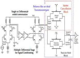
ABSTRACT: The track-and-hold amplifier (THA) using fully-differential architecture to mitigate common-mode
noise and suppress even-order harmonics is presented. CMOS switch and dummy switches are adopted to achieve high speed and good linearity. A cross-coupled pair is used in the input buffer to suppress the charge injection and clock feedthrough. Both the input and output buffers use an active inductor load to achieve high signal bandwidth. The THA is realized with 0.18 micro meter or 45nm SiGeBiCMOS technology using only CMOS devices at a 1.8 V voltage supply and with a core area of 0.024 mm2.Itis shown that both the thermal noise and shot noisecontribute to the TH amplifier (THA) at ultra-highfrequency. Simulations also locate the major noisecontributor in the SEF THA. Approximate expressions for the output noise of the major noise contributor of the THA are derived and the numericalexperiment of the output noise is presented.
KEYWORDS: Track and hold amplifier, BiCMOSswitched emitter follower, ultra-high speed, noise location and
noise model.
I. INTRODUCTION
The high-speed analog-to-digital converters(ADCs)is the heart of the optic equalizer[1]. TheTHA is a crucial building block in ADCs since it makes agreat impact on the dynamic performance of ADCs. Toachieve high speed operation, the open loop architectureswitched emitter follower is chosen for THA[1]. Noise isone of the important factors that limit the dynamic rangeof THA. As a result, it reduces the achievable resolutionof the circuit. Therefore it is necessary to minimize thiseffect in order to improve the circuit performance. Theoretical noise analysis and numerical examples for switchedcapacitor amplifier circuits are present in [2]. To the bestof our knowledge, noise analysis in SiGe HBT SEF THAhas not been reported in the literature.In this paper, we analyze the noise of major noise contributor in the hold mode of THA with the SEF configuration. Simulation and analysis show that, at ultra-high frequency, both the thermal noise and shot noisecontribute to the output noise, the flicker noise can beignored. Section 2 describes the noise in a SEF THA forultra-high speed application.
With CMOS technology, downscaling of the conversionspeed of the ADC has rapidly been developing, implying thatthe T/H has to process input signals at increasingly higherspeed. Thus, in order to guarantee the accuracy of the T/Hat such high speed of operation, a larger bandwidth becomesnecessary, leading, on the other hand, to significant power dissipation, which might become the dominant factor in the wholeADC power consumption. In this brief, a power--speed high-accuracy T/H amplifier will be presented. Theproposed power-switching (P-S) technique provides a rapidswitching operation in order to avoid the static power dissipation of the T/H without degrading the output voltage swing.Meanwhile, by using the technique, the tracking speed andaccuracy of the T/H are enhanced as well.
ISSN(Online) : 2319-8753 ISSN (Print) : 2347-6710
International Journal of Innovative Research in Science,
Engineering and Technology
(An ISO 3297: 2007 Certified Organization)
Vol. 5, Issue 3, March 2016
thebroadband designs to extend the operation bandwidth. Moreover, the distributed amplifier (DA) can also be employed inthe input buffer to improve the bandwidth and input return loss.The DA has been employed in a CMOS track-and-hold amplifier [14], and the input bandwidth can be up to the several gigahertz range.
III. TRACK-AND-HOLD STAGE
The track-and-hold stage is designed using the switched capacitor technique, and the schematic is shown in Fig. 2. Twopaths are for the differential inputs, and the switch consists ofone PMOS transistor ( or ) and a dummy PMOS transistor ( or ). The dummy PMOS transistors are used toeliminate the issue of charge injection when the track-and-holdstage is operated in the hold mode. To maximize the bandwidthand minimize the insertion loss of the track mode, the transistorsize of the switch should be properly designed. The even harmonics can be intrinsically cancelled due to the differential operation. For the consideration of the linearity and SFDR, theodd harmonics should be carefully considered, especially forthe third-order harmonic. The third-order harmonic distortion(HD3) is defined as the power ratio between the fundamentaland third harmonic. The HD3 of the switch can be expressed as
Where is the input angular frequency.is the transconductance delay of the transistor and it can be obtained basedon the circuit simulation. The track-mode bandwidth of the switch is the single-end input swing is thetransistor threshold voltage, and the typical value is 0.3 V and is an appropriate dc value about 0.5 Vof the input signal. The calculated HD3 and transconductancedelay versus total gate width is plotted in Fig. 3, where theinput frequency is 5 GHz with an amplitude swing of 0.3 Vp-p.The HD3 and the transconductance delay decrease as the gatewidth increases, but the bandwidth degrades due to the parasiticcapacitor of the transistor. Therefore, the design tradeoff of gatewidth is between the HD3 and the bandwidth. To completelyinvestigate the design tradeoff, the 65-nm CMOS switch witha holding capacitance, , of 390 fF is simulated under thesampling and holding conditions. To minimize the chip area,the holding capacitor can be designed using the input gateparasitic capacitor of the transistor. The capacitance is basedon the input parasitic capacitance of the output buffer. Thesimulated turn-on bandwidth, insertion gain, and HD3 versustotal gate width for the track-and-hold switch are plotted inFig. 4, where the input frequency is 5 GHz with an amplitudeswing of 0.3 Vp-p and the sampling rate is 10 GS/s. For thesimulation setup of the switch, the input termination resistanceis50 , and the output termination network is a 50- resistorparallel with a 390-fF holding capacitor. For the dynamicallysample-and-hold operation, the insertion gain increases as thetotal gate width increases, and the turn-on bandwidth decreases.The minimum HD3 occurs when the total gate width is closeto 60 m. To achieve good linearity with enough bandwidth,a total gate width of 16 4 m is selected as the preliminarydesign.
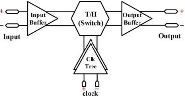
Fig 1.Block diagram of a typical track-and-hold circuit.
ISSN(Online) : 2319-8753 ISSN (Print) : 2347-6710
International Journal of Innovative Research in Science,
Engineering and Technology
(An ISO 3297: 2007 Certified Organization)
Vol. 5, Issue 3, March 2016
amplifiers feature high SFDR and low THDwith compact chip area, and they can be compared with thepreviously reported state-of-the-art track-and-hold amplifiers.The spiral inductor and the transmission line are adopted forthe peaking elements. The thin-film microstrip line (TFML) isadopted for the circuit connection to further reduce unwantedcoupling effect and chip size, the top metal (M9) is designed as asignal line, and the bottom metal (M1) is designed as a groundedplane.The spiral inductor and the transmission line are adopted forthe peaking elements. The thin-film microstrip line (TFML) isadopted for the circuit connection to further reduce unwantedcoupling effect and chip size, the top metal (M9) is designed as asignal line, and the bottom metal (M1) is designed as a groundedplane.
Fig 2.Schematic of the track-and-hold stage.
All the passive components, including transmission lines,inductors, capacitors, and resistors, are simulated with a fullwave electromagnetic (EM) simulator [21].The track-and-hold amplifier is usually composed of a differential input buffer, a differential output buffer, a track-and-holdstage, and a differential clock buffer. The input and output bufferis used to maintain the voltage swing of the input signal overoperation frequency, and the buffers should have good linearity,high SFDR, and broadband and flat voltage gain. In general, thevoltage gain of the buffer can be close to 0 dB. The switch isoften employed in the track-and-hold stage to perform the inputsignal tracking and sampling. The track-and-hold switch shouldhave low turn-on insertion loss, high turn-off isolation, and goodlinearity. To achieve the high-speed operation, the bandwidth ofthe track mode should be wide enough as the switch is turnedon. The clock buffer is designed to make the voltage swing ofthe clock signal large enough, and the track-and-hold switch canbe normally operated in turn-on and turn-off states. In addition,the rising and falling times of the clock can be reduced using theclock buffer for high-speed sampling, and the signal-to-noiseratio and resolution would be further improved.
The schematic of the 45-nm CMOS track-and-hold amplifier is shown in Fig. 3, and the design parameters are summarized in Table I. The track-and-hold amplifier consists of adifferential input buffer, a differential output buffer, a differential track-and-hold switch, and a differential clock buffer.
Fig 3.Schematic of the 45-nm CMOS track-and-hold amplifier designed using cascode buffers with inductive peaking.
ISSN(Online) : 2319-8753 ISSN (Print) : 2347-6710
International Journal of Innovative Research in Science,
Engineering and Technology
(An ISO 3297: 2007 Certified Organization)
Vol. 5, Issue 3, March 2016
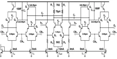
hold-mode feed-through, and distortion. Thebody bias technique can also be employed in the switch to enhance the linearity due to the reduction of the nonlinear junctioncapacitances [25]. The input parasitic capacitances of the outputbuffer and are also performed as the hold-mode element to further reduce the chip size. The input and output buffersare designed using a two-stage differential pair to enhance thecommon-mode rejection ratio. The first stage is designed usingthe CS amplifier with a source resistor to enhance the linearity,and the second stage is designed using the cascode amplifierwith inductive peaking to improve the voltage headroom. Thetransistors of the buffers are operated in the class-A region forhigh linearity. The drain and source resistors, and , areselected about 2:1 ratio to achieve unity dc gain. The drain andsource inductances, and , are designed between 100 and150 pH to further improve the gain roll-off at high frequency.The schematic of the 45-nm BICMOS track-and-hold amplifier is shown in Fig4, which consists of a differential switch, adifferential input buffer, and a differential output buffer.
Fig 4.Schematic of the 45nm BICMOS track-and-hold amplifier designed using the distributed input buffer.
The circuittopology and design method of the switch is similar to the45-nm BICMOS track-and-hold amplifier. The CS–CG cascade amplifier with inductive peaking is also adopted for the outputbuffer to enhance the voltage headroom and the bandwidth.The input buffer is designed using a two-stage DA to furtherimprove the operation bandwidth and the input return loss.The inductances for the drain and gate artificial transmission linesshould be properly designed to maximize the bandwidth withflat frequency response. The layouts of and are designed using a differential spiral inductor to reduce the chiparea and enhance the common-mode rejection ratio. The lossof the switch is further compensated by the input buffer, andthe voltage gain can be designed by selecting the transistor sizeor the dc bias of the gain cell. Several current sources, currentmirror, and bypass networks are also included in the chip forthe dc bias.
IV. RESULTS
Fig 5.Schematic of the 45-nm CMOS track-and-hold amplifier designed using cascode buffers with inductive peaking.
V. CONCLUSION
ISSN(Online) : 2319-8753 ISSN (Print) : 2347-6710
International Journal of Innovative Research in Science,
Engineering and Technology
(An ISO 3297: 2007 Certified Organization)
Vol. 5, Issue 3, March 2016
low THD. Moreover, they can beapplied to the front-end sample and hold applications, such asa high-speed low-power hand-held oscilloscope and broadbanddata converter.
REFERENCES
[1] A. Boni, A. Pierazzi, and C. Morandi, “A 10-b 185-MS/s track-andhold in 0.35- m CMOS,” IEEE J. Solid-State Circuits, vol. 36, no. 2,pp. 195– 203, Feb. 2001.
[2] X. Li, W.-M. Kuo, Y. Lu, R. Krithivasan, J. D. Cressler, and A. J.Joseph, “A 5-bit, 18 GS/sec SiGe HBT track-and hold amplifier,”in IEEE Compound Semicond. Integr. Circuit Symp., Oct. 2005, pp.105–108.
[3] H.-G. Wei, U.-F. Chio, Y. Zhu, S.-W. Sin, S.-P. U, and R. P. Martins,“A rapid power-switchable track-and-hold amplifier in 90-nm CMOS,”IEEE Trans. Circuits Syst. II, Exp. Briefs, vol. 57, no. 1, pp. 16–20, Jan.2010.
[4] J. Lee et al., “A 6-b 12-GSamples/s track-and-hold amplifier in InPDHBT Technology,” IEEE J. Solid-State Circuits, vol. 38, no. 6, pp.1533– 1539, Jun. 2003.
[5] Y. Bouvier, A. Ouslimani, A. Konczykowska, and J. Godin, “A1-GSample/s, 15-GHz input bandwidth master–slave track-and-holdamplifier in InP DHBT technology,” IEEE Trans. Microw. TheoryTechn., vol. 57, no. 12, pp. 3181–3187, Dec. 2009.
[6] Y. Bouvier, A. Ouslimani, A. Konczykowska, and J. Godin, “A 40G samples/s InP-DHBT track-and-hold amplifier with high dynamicrange and large bandwidth,” in 8th Int. Commun. Syst., Networks, Digital Signal Process. Symp., Jul. 2012, pp. 1–4.
[7] J. Deza et al., “A 50-GHz-small-signal-bandwidth 50 GSa/strack&hold amplifier in InP DHBT Technology,” in IEEE MTT-S Int.Microw. Symp. Dig., Jun. 2012, pp. 17–22.
[8] J. Deza, A. Ouslimani, A. Konczykowska, A. Kasbari, and J. Godin,“A 4 GSa/s, 16-GHz input bandwidth master-slave track-and-holdamplifier in InP DHBT Technology,” 20th Telecommun. Forum, pp.502–505, Nov. 2012.
[9] J. Deza, A. Ouslimani, A. Konczykowska, A. Kasbari, J. Godin, and G.Pailler, “70 GSa/s and 51 GHz bandwidth track-and-hold amplifier inInP DHBT process,” Electron. Lett., vol. 49, pp. 388–389, Mar. 2013.
[10] S. Shahramian, A. C. Carusone, and S. P. Voinigescu, “Design methodology for a 40-GSamples/s track and hold amplifier in 0.18- m SiGeBiCMOS technology,” IEEE J. Solid-State Circuits, vol. 41, no. 9, pp.2233–2240, Sep. 2006.
[11] X. Li, W.-M. L. Kuo, and J. D. Creeler, “A 40 GS/s SiGe track-andhold amplifier,” in IEEE Bipolar/BiCMOS Circuits Technol. Meeting,Oct. 2008, pp. 1–4.
[12] S. Shahramian, S. P. Voinigescu, and A. C. Carusone, “A 35-GS/s,4-bit flash ADC with active data and clock distribution trees,” IEEEJ. Solid-State Circuits, vol. 44, no. 6, pp. 1709–1720, Jun. 2009.
[13] M. Buck, M. Grözing, M. Berroth, M. Epp, and S. Chartier, “A 6 GHzinput bandwidth 2 Vpp-diff input range 6.4 GS/s track-and-hold circuit in 0.25 m BiCMOS,” in IEEE RFIC Symp. Dig., Jun. 2013, pp.159–162.
[14] H. Orser and A. Gopinath, “A 20 GS/s 1.2 V 0.13 m CMOS switchedcascode track-and-hold amplifier,” IEEE Trans. Circuits Syst. II, Exp.Briefs, vol. 57, no. 7, pp. 512–516, Jul. 2010.