2D and 3D photonic crystals: synthesis, characterization
and topological phenomenon
Thesis by
Siying Peng
In Partial Fulfillment of the Requirements for the
degree of
Doctor of Philosophy
CALIFORNIA INSTITUTE OF TECHNOLOGY
Pasadena, California
2018
© 2018
Siying Peng
ORCID: [0000-0002-1541-0278]
iii
ACKNOWLEDGEMENTS
First, I would like to thank my thesis advisor, Professor Harry A. Atwater, for his
guidance and support throughout the entire work. This thesis reflects efforts
explor-ing immature ideas and learnexplor-ing experience from unproductive experiments. I am
grateful to Harry for giving me enough freedom to explore, while always offering his endless enthusiasm, patience and support. Scientifically, I have a deep respect
for Harry’s intellectual abilities. He provides sometimes the most unexpected but
extremely valuable insights, which inspired me to think more creatively. I am also
thankful for all the opportunities Harry had provided, such as attending conferences
and collaborations.
I would like to thank my thesis committee members Professor James Eisenstein,
Professor Andrei Faraon and Professor Gil Refael. Gil have provided much valuable
feedback regarding research and career opportunities. Both Andrei and Jim have
been a pleasure to interact with, and I appreciate their invaluable advice.
This thesis would not have been possible without all the contributions from my
collaborators. I would like to thank Professor Albert Polman of AMOLF, the
FOM-institute, for his constant support and encouragement. I started collaborating with
Albert in 2013 on characterizing plasmon dispersions of metallic nanoparticles
(de-scribed in Chapter 4). We moved on to work with silicon nanostructures (de(de-scribed
in Chapter 5 and Chapter 6), which hopefully will be productive towards realizing
topologically protected edge states.
I am grateful to Professor Paul Braun of University of Illinois at Urbana–Champaign.
Paul provided valuable insights on 3D photonic crystal fabrication and offered col-laboration opportunities on making high refractive gyroid structures, without which
Chapter 2 and Chapter 3 would not be possible.
I am thankful to Professor William Andrew Goddard III, who I had collaborated
with from 2012 to 2013 for work described in Chapter 7. Bill continued to offer
valuable career advice throughout my years at Caltech which I am extremely grateful
for.
Many thanks to Runyu Zhang of University of Illinois at Urbana–Champaign, who
performed static CVD depositions and contributed ideas for work done in Chapter
2 and Chapter 3. We have been through many ups and downs of the project, Runyu has always been extremely encouraging and supportive. I would like to thank Dr.
on angle resolved mid-infrared characterization. Phil contributed enormously
to-wards designing and optimizing the set up, and Juan offered his incredible expertise to debug whenever we encounter difficulties. Emil Khabiboulline, who is now a
graduate student at Harvard University, was also an indispensable member of the
angle resolved mid-infrared characterization team. Emil wrote the entire Python
code that automated the measurement, as well as developed the initial mpb code for
bandstructure projection. Valerian Chen, who is now a graduate student at Oxford
University, contributed a lot to the initial design, fabrication, and characterization
work. Vitoria Barim, a undergraduate student from university of Helsinki, worked
with me last summer on optimizing the angle resolved set up.
I would like to thank Benjamin Brenny, Toon Coenen, Sondra Hellstrom, Sophie Meuret, and Nick Schilder. Sophie, Nick, and Toon from AMOLF have been
in-credibly helpful with the CL experiment and data analysis; Chapter 5 and Chapter
6 would not have been possible without their help. The CL work in Chapter 4 was
done with Benjamin and Toon’s help. Sondra, who was a postdoc in Harry’s group,
developed a recipe for fabricating metallic nano-pillars.
I would like to thank Professor Matthew Sheldon, with whom I coauthored the paper
described in Chapter 7. In addition, Matt mentored me through my first two years at
Caltech which I am extremely grateful for. I am also thankful to Wei-Guang Liu and
Andres Jaramillo-Botero who performed electronic states simulations described in Chapter 7.
I have benefited greatly from interacting with past and current members of the
A-team, I would like to thank everyone for their contributions. In particular, I would
like to acknowledge Dr. James Fakonas for teaching me everything I know about
clean room fabrication. Dr. Yulia Tolstova and Dr. Seokmin Jeon taught and helped
me a lot with high vacuum equipments. I would like to thank Tiffany Kimoto,
Jennifer Blankenship, Liz Jennings, and Lyann Lau, who keep the Atwater group
running smoothly.
Special thanks to Fan Liu, who has helped, supported and believed in me in every aspect for the past five years. I am also grateful for the friendship with Tian Zhong
and Mingwu Lu. There were lots of good memories from the weekly Friday dinner.
I would like to thank my grandparents, Xiaojun Kan and Zhongmin Peng, for their
unconditional love. Family members who passed away, including my father Yong
Peng (2003), grandmother Yide Qin (1997), and grandfather Shiming Xiang (2012),
were very influential on my early interests in science. Finally and most importantly,
v
unconditionally supported my dreams. This thesis is dedicated to her.
Siying Peng
May 2017
vii
ABSTRACT
Topological photonics has become an increasingly popular research topic in the field
of nanophotonics in recent years. Topological phases of light provide opportunities
to manipulate light propagation efficiently at the nanoscale volume. Performance
of conventional optical elements are limited by back-reflection and bending losses, which hinder their prospect of large scale integration. Topological protection enables
unidirectional excitation of edge states or surface states without leaking into the bulk,
as well as suppression of scattering when encountering defects and corners. With
such advantages, topological photonic elements may surpass conventional photonic
design for future generations of ultra-compact efficient computing, imaging, and
sensing applications. Due to limitations of fabrication and characterization
tech-niques, previously experimental efforts on topological photonics have been carried
out with 2D micron-scale optical design or at the microwave wavelength.
This thesis contributes to the experimental development of topological photonics
in two aspects: first, how to fabricate and characterize 3D photonic crystals and
therefore extend topological protection into the 3D (Chapters 2-3); and second, how
to realize nanoscale topological protection in the visible frequencies (chapters 4-6).
Specifically, Chapter 2 reports fabrication of 3D single gyroid structures
com-posed of a-Si and FTIR characterization of a photonic bandgap at the mid-infrared
wavelength. This is the foundation to investigate more complex morphologies to
introduce topologically nontrivial photonic states. Chapter 3 describe properties of double gyroid photonic crystals, followed by angle resolved characterization method
in the mid-infrared. Double gyroid photonic crystals can be designed to possess
quadratic degeneracy points, Weyl points, and line nodes. Since Weyl points have
non-zero Chern numbers, surface states are topologically protected in double gyroid
photonic crystals with parity breaking symmetry. The angle resolved
characteriza-tion method could be utilize to resolve both Weyl points and surface states. Chapter
4 depicts design, fabrication, and characterization of Dirac-like surface plasmon
dispersions in metallic nano-pillars. Chapter 5 presents experimental investigation
of coupled silicon Mie resonators, which is the first step towards topological design based on inter-lattice sites coupling in the next chapter. Chapter 6 details photonic
bandstructure from angle-resolved cathodoluminescence measurements. We
lattices, as well as zigzag and arm-chaired edges of domain boundaries. Chapter 7
outlines a method to optically enhance dissociation of hydrazine molecules using ultraviolet plasmons, and attempts to use this method for low temperature GaN
ix
PUBLISHED CONTENT AND CONTRIBUTIONS
[1] Siying Peng et al. “Three-Dimensional Single Gyroid Photonic Crystals with a Mid-Infrared Bandgap”. In:ACS Photonics3.6 (June 2016), pp. 1131–1137. doi:10.1021/acsphotonics.6b00293.
S.P. participated in the design of the project, performed simulations, pre-pared the sample, collected the data, and participated in the writing of the manuscript.
[2] “Ultraviolet surface plasmon-mediated low temperature hydrazine decom-position”. In: Applied Physics Letters 106.2 (Jan. 2015), p. 023102. doi:
10.1063/1.4905593.
TABLE OF CONTENTS
Acknowledgements . . . iii
Abstract . . . vii
Published Content and Contributions . . . ix
Table of Contents . . . x
List of Illustrations . . . xii
List of Tables . . . xxi
Chapter I: Introduction . . . 1
Chapter II: Single gyroid photonic crystals with a mid-infrared bandgap: synthesis and Fourier transform infrared spectroscopy characterization . . 3
2.1 Introduction . . . 3
2.2 Design and fabrication of a-Si single gyroid photonic crystals . . . . 5
2.3 Fourier transform infrared spectroscopy characterization . . . 6
2.4 Discussion and conclusion . . . 7
Chapter III: Double gyroid photonic crystals: synthesis and angle resolved mid-infrared characterization . . . 12
3.1 Introduction . . . 13
3.2 Frequency domain simulation method of double gyroids . . . 14
3.3 Three-dimensional band structure projection onto a two-dimensional plane . . . 15
3.4 Synthesis of double gyroid photonic crystals . . . 15
3.5 Angle resolved mid-infrared spectroscopy . . . 19
3.6 Conclusions and outlook . . . 21
Chapter IV: Dirac-like plasmons in silver nanopillar honeycomb lattices: design, fabrication and cathodoluminescence characterization . . . 25
4.1 Introduction . . . 26
4.2 Tight binding model . . . 26
4.3 Full wave finite-different time-domain design of Dirac-like plasmons 27 4.4 Fabrication of silver nanopillar honeycomb lattices . . . 29
4.5 Cathodoluminescence characterization of Dirac-like plasmons . . . . 30
Chapter V: Mie resonators: resonances and couplings . . . 34
5.1 Introduction . . . 34
5.2 Sample Fabrication . . . 35
5.3 Resonances and coupling of Mie resonators with aspect ratio=1 . . . 35
5.4 Resonances and coupling of Mie resonators with aspect ratio=0.65 . 37 5.5 Asymmetric dimers . . . 38
5.6 Coupling of hexamers and honeycomb lattices . . . 39
5.7 Conclusions and outlook . . . 41
xi
6.1 Introduction . . . 45
6.2 Dirac-like bandstructures of honeycomb lattice and edge states . . . . 46
6.3 Angle-resolved cathodoluminescence characterization of photonic bandstructures . . . 47
6.4 Photonic band structures in the bulk and on the edges . . . 49
6.5 Conclusions . . . 50
Chapter VII: Ultraviolet surface plasmon-mediated low temperature hydrazine decomposition and growth of GaN . . . 54
7.1 Motivation . . . 54
7.2 N-H bond energy of the N2H4molecule . . . 55
7.3 FDTD simulation of aluminum plasmonic grating . . . 57
7.4 Fabrication of aluminum grating by nanoimprint lithography and UV characterization . . . 57
7.5 Low temperature hydrazine decomposition: experimental set up and characterization . . . 59
7.6 Experimental set up of ultraviolet plasmon assisted low temperature GaN growth . . . 62
7.7 XRD, XPS, EDS, and Raman characterization of GaN film synthe-sized at low temperature condition . . . 63
7.8 Conclusions . . . 66
Bibliography . . . 68
Appendix A: Chapter 2 methods and supplementary information . . . 77
A.1 Full Wave Band Structure Simulation . . . 77
A.2 Sample Fabrication . . . 77
A.3 FTIR Characterization . . . 77
A.4 Full Wave Simulation on deformed Crystals . . . 78
A.5 Optical constants of deposited materials . . . 78
LIST OF ILLUSTRATIONS
Number Page
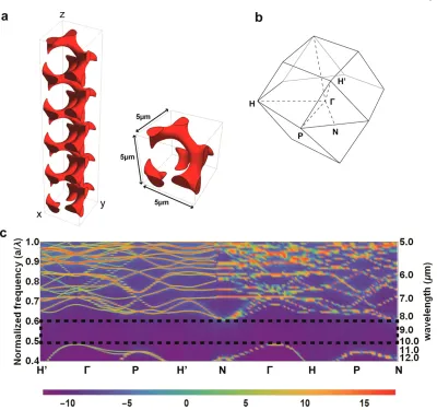
2.1 Single gyroid structure and photonic bandstructure simulation. (a)
Stacks of unit cells of single gyroid structure. (b) bcc Brillouin
zone. (c) Photonic band structure of a-Si single gyroid from full
wave simulations, with unit cell size of 5 µm in x, y, and z directions.
The color map is proportional to the logarithm of the density of states. 4
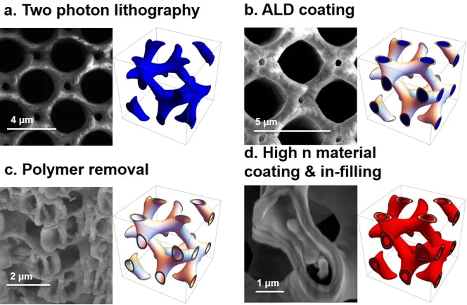
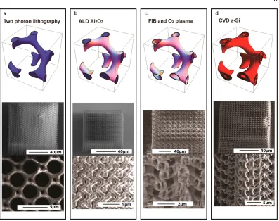
2.2 Fabrication procedures of gyroid photonic crystals. (a) Two-photon
lithography to define a sacrificial polymer scaffold of the gyroid structure. (b) Atomic layer deposition of Al2O3to coat the polymer
structure. (c) Focused ion beam milling to remove the sides of the
structure, followed by oxygen plasma to remove the polymer, leaving
a hollow alumina structure. (d) Chemical vapor deposition of a-Si to
coat and in-fill the hollow alumina structure. . . 6
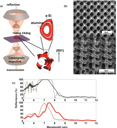
2.3 FTIR characterization of bandgaps. (a) Fourier transform infrared
spectroscopy experimental configuration. (b) SEM images of a
hol-low gyroid at (001) crystal orientation with a-Si (150 nm)/Al2O3(40
nm)/a-Si (150 nm) layers. (c) Reflectance spectrum from full wave simulations of a hollow gyroid at (001) crystal orientation with a-Si
(100 nm)/Al2O3 (40 nm)/a-Si (100 nm) layers (gray dashed line),
reflectance spectrum from full wave simulations of a trapezoidal
hol-low gyroid at (001) crystal orientation with a-Si (100 nm)/Al2O3(40
nm)/a-Si (100 nm) layers (black dashed line), FTIR measurement of
a hollow gyroid with a-Si (100 nm)/Al2O3 (40 nm)/a-Si (100 nm)
layers (red dashed line), and FTIR measurement of a hollow gyroid
with a-Si (150 nm)/Al2O3(40 nm)/a-Si (150 nm) layers (red dashed
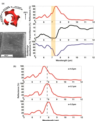
line). . . 8 2.4 FTIR characterization of single gyroids. (a) Reflectance,
transmit-tance, and scattering + absorbance from a single gyroid structure
with unit cell size of 4.5 µm and a total of 20 × 20 × 10 cells. (b)
Comparison of reflection spectra of samples with unit cell sizes of
xiii
2.5 Photonic band structure simulation. Photonic band structure of a
single gyroid consists of a-Si (100 nm)/Al2O3(40 nm)/a-Si (100 nm)
layers from full wave simulations, with unit cell size of 4.5 µm in x,
y, and z directions. Bands in between the orange lines are accessible
through FTIR characterization shown in . . . 10
3.1 (a) BCC Brillouin zone (b) Double gyroids (c) Double gyroids with
an airsphere which breaking parity symmetry (d) Double gyroids
with two airspheres . . . 13
3.2 Band structures of double gyroids with unit cell size of 4.68µm . . . 15
3.3 Band structures of double gyroids with unit cell size of 4.68µm (a)
Double gyroids with quadratic point degeneracy (indicated by yellow circles) (b) Double gyroids with Parity breaking symmetry, which
give rise to a pair of Weyl points. The Parity breaking airsphere
is indicated by the yellow circle in the unit cell. Weyl points are
indicated by the yellow circles along Γ-N11 and Γ-H3. (c) Double gyroids with two air spheres in one unit cell (indicated by yellow
circles). Line nodes are indicated by yellow circlesΓ-N11 andΓ-H3. 16 3.4 Band structures of double gyroids with unit cell size of 4.68µm (a)
Double gyroids with parity breaking symmetry by an airsphere, which
give rise to a pair of Weyl points. The parity breaking airsphere is indicated by the yellow circle in the unit cell. Weyl points are
indicated by the yellow circles along Γ-N11 and Γ-H3. (b) Double gyroids with Parity breaking symmetry by a thin cylinder, which also
give rise to a pair of Weyl points along the same symmetry directions.
The parity breaking cylinder is placed at the spatial position as the
airsphere. . . 16
3.5 Illustration of 3D band structure projection onto a 2D plane, along
theGamma-H1 direction. . . 17
3.6 Projection of double gyroid band structures along the [001] direction. 17 3.7 Projection of Weyl points band structures along the [001] direction. . 18
3.8 Projection of line nodes band structures along the [001] direction. . . 18
3.9 Synthesis of three-dimensional photonic crystals with high-refractive
3.10 FTIR characterization of double gyroids: (a) Illustration of FTIR set
up (b) Reflectance spectrum from single gyroid (red), double gyroids (blue) and double gyroids with parity breaking symmetry (green) (c)
SEM images of single gyroid (red), double gyroids (blue), and double
gyroids with parity breaking symmetry (green) . . . 21
3.11 Photo of angle resolved characterization set up . . . 22
3.12 Angle resolved characterization set up for normal incidence reflectance
measurement . . . 22
3.13 Angle resolved characterization set up for off normal incidence
mea-surement . . . 23
3.14 Fabry-Perot resonance from silicon substrate (a) reflectance (b) trans-mittance (c) simulated reflectance . . . 23
3.15 Double gyroid photonic band structures (a) simulation (b)
experi-mental characterization . . . 24
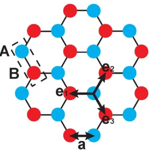
4.1 Honeycomb lattices with lattice constant a and lattice vectors e1,e2,
ande3; one unit cell of the lattice has two lattice sites: A and B. . . . 27
4.2 Dirac-like surface plasmon bandstructures: (a) three-dimensional
bandstructures with six Dirac points, (b) two-dimensional
bandstruc-tures along high symmetry directions of the hexagonal lattice . . . . 27
4.3 (a) Full wave simulations of bandstructures of silver nanopillars in honeycomb lattices (r=80nm, h=160nm with a Drude model
approx-imation for silver dielectric constants) (b) Degree of hybridization
(∆λ) as a function of lattice sites separation and aspect ratio of indi-vidual lattice sites . . . 29
4.4 Electric field distribution of silver nanopillars at the M point and the
K point . . . 29
4.5 Opening a bandgap at the Dirac point (a) Gap size as a function
of lattice distortions (b) Band structures of distorted lattice with a
band gap at the Dirac point (r=80nm, h=160nm with a Drude model approximation for silver dielectric constants) . . . 30
4.6 Fabrication method: 1. Spin bottom two layers of ebeam resist
(bottom layer: PMMA 495, top layer: PMMA 950), 2. Electron
beam lithography to define honeycomb patterns and development of
exposed areas 3. Electron beam deposition of germanium as the
xv
4.7 SEM images of fabricated silver nanopillars in honeycomb lattices
(a) top view (b) side view . . . 31 4.8 Angle resolved cathodoluminescence of a single silver pillar at 650nm 32
4.9 Angle resolved cathodoluminescence of a dimer pair of silver pillars
at 650nm . . . 33
4.10 Angle resolved cathodoluminescence of silver pillars in honeycomb
lattices at (a) 800nm (b) 750nm . . . 33
5.1 Fabrication of Mie resonators on 10nm free-standing Si3N4
mem-branes: (a) Epitaxial lift off of a single crystalline silicon film from
an SOI wafer (b) Placement of the silicon film on a 10nm
free-standingSi3N4membrane (c) Spin a layer of ZEP520 on the silicon
film (d) Electron beam lithography on the ZEP520 film (e) Electron
beam curing of the ZEP520 film as an etching mask (f) Reactive
ion beam etching of the silicon film (g) Oxygen plasma cleaning to
remove ZEP520 . . . 36
5.2 Single Mie resonator: (a) Scattering cross section of a single silicon
Mie resonator with radius of 65nm and height of 130nm (b) Electric
field intensity distribution of the top XY plane at 494nm (c)
Elec-tric field intensity distribution of the center XZ plane at 494nm (d)
Electric field intensity distribution of the top XY plane at 596nm (e) Electric field intensity distribution of the center XZ plane at 596nm . 38
5.3 Coupled Mie resonators (a) Scattering cross section of dimer silicon
Mie resonators with radius of 65nm and height of 130nm and distance
of 40nm from edge to edge (b) Electric field intensity distribution of
the top XY plane at 484nm (c) Electric field intensity distribution
of the center XZ plane at 484nm (d) Scattering cross section of :
a single silicon Mie resonator with radius of 65nm and height of
130nm (dashed blue ); dimer silicon Mie resonators at distance of
10nm apart (lightest blue); dimer silicon Mie resonators at distance of 15nm apart (second lightest blue); dimer silicon Mie resonators
at distance of 20nm apart (third lightest blue); dimer silicon Mie
resonators at distance of 40nm apart (fourth lightest blue) (e) Electric
field intensity distribution of the top XY plane at 616nm (f) Electric
5.4 Cathodoluminescence characterization of coupled Mie resonators (a)
CL spectrum of a single particle of radius 65nm and height 130nm at the center (left), side (middle), CL map at 571nm (right) (b) Dimers
of 40nm apart: Cl spectrum at the center (left), side (middle), CL
map at 599nm (right) (c) Dimers of 20nm apart: Cl spectrum at the
center (left), side (middle), CL map at 624nm (right) (d) Dimers of
15nm apart: Cl spectrum at the center (left), side (middle), CL map
at 644nm (right) (e) Dimers of 10nm apart: Cl spectrum at the center
(left), side (middle), CL map at 689nm . . . 40
5.5 Connected Mie resonators: (a) CL spectrum of a single particle of
radius 65nm and height 130nm at the center (left), side (middle), CL map at 571nm (right) (b) Dimers of 10nm apart: Cl spectrum at the
center (left), side (middle), CL map at 689nm (b) Connected dimers:
Cl spectrum at the center (left), side (middle), CL map at 609nm . . . 41
5.6 Single Mie resonator: (a) CL spectrum of a single particle of radius
100nm and height 130nm at the center (b) CL spectrum of a single
particle of radius 100nm and height 130nm at the side (c) CL intensity
map at 422nm (d) CL intensity map at 483nm (e) CL intensity map
at 568nm (f) CL intensity map at 624nm (g) CL intensity map 688nm 42
5.7 Coupled Mie resonators: (a) CL spectrum of a single particle of radius 100nm and height 130nm at the side (b) CL spectrum of dimer
particles on the side (c) CL intensity map at 423nm (d) CL intensity
map at 483nm (e) CL intensity map at 558nm (f) CL intensity map
xvii
5.8 Asymmetric dimers: (a) CL spectrum of a single particle of radius
100nm and height 130nm on the side (b) CL spectrum of a asymmetric dimer 40nm apart (r1=100nm,r2=65nm), excitation point on the side
of the r1=100nm particle (c) CL spectrum of a asymmetric dimer
200nm apart (r1=100nm, r2=65nm), excitation point on the side of
ther1=100nm particle (d) CL spectrum of a single particle of radius
65nm and height 130nm on the side (e) CL spectrum of a asymmetric
dimer 40nm apart (r1=100nm,r2=65nm), excitation point on the side
of the r1=65nm particle (f) CL spectrum of a asymmetric dimer
200nm apart (r1=100nm, r2=65nm), excitation point on the side of
ther1=65nm particle (g) CL intensity map at 558nm of the 40nm apart
dimer (h) CL intensity map at 614nm of the 40nm apart dimer (i) CL
intensity map at 694nm of the 40nm apart dimer (j) CL intensity map
558nm of the 200nm apart dimer (k) CL intensity map 694nm of the
200nm apart dimer (l) CL intensity map 693nm of the 200nm apart
dimer . . . 43
5.9 Hexamers and honeycomb lattice modes: (a) Lattice l at 426nm,
modes in the center (b) Lattice L at 664 nm, anti-bonding mode (c)
Lattice L at 750 nm, bonding mode (d) SEM image of lattice l (e)
Hexamer l at 426 nm (f) Hexamer l at 664 nm (g) Hexamer l at 750 nm (h) SEM image of hexamer l (i) Lattice s at 452 nm (j) Lattice
s at 518 nm (k) Lattice s at 750 nm (l) SEM image of lattice s (m)
Hexamer s at 452 nm (n) Hexamer s at 518 nm (o) Hexamer s at
750nm (p) SEM image of hexamer s . . . 44
6.1 (a) Honeycomb lattice with lattice constant R1 for the smallest unit
cell (diamond shaped dashed line), and triangular lattice with lattice
constant R2 with the hexagonal shaped unit cell (dashed cell) (b)
First Brillouin zone of the honeycomb lattice (dashed line), reduced
Brillouin zone of the supercell triangular lattice (solid line) (c) Band structures of a honeycomb lattice in the first Brillouin zone (d) Band
structures of a supercell triangular lattice with a band gap (R2=2.9R1)
(e) Edge states at the Zigzag edge within the bandgap . . . 47
6.2 Electron beam induced bands asymmetry: (a) 630 – 670 nm (b) 580
– 620 nm (c) 530 – 570 nm (d) 480 – 520 nm (e) 430 -470 nm (d)
6.3 Mapping band structures in the Brillouin zone: (a) Honeycomb
lat-tices s 630-670nm; (b) Topologically gapped latlat-tices s 630-670nm; (c) Trivially gapped lattices s 630-670nm; (d) Zigzag edges lattice
s 630-670nm; (e) Arm-chaired lattice s 630-670nm; (f) Honeycomb
lattices l 580-620nm; (g) Topologically gapped lattices l 580-620nm;
(h) Trivially gapped lattices l 580-620nm; (i) Zigzag edges lattices l
580-620nm; (j) Arm-chaired lattices l 580-620nm . . . 50
6.4 Spectral resolved photonic bands lattice s (r1=65nm, h=150nm,
triv-ial gap: R1=246nm, R2=444nm, factor=3.12): (a) 0 degrees
topo-logical gap (b) 15 degrees topotopo-logical gap (c) 30 degrees topotopo-logical
gap (d) 45 degrees topological gap (e) 60 degrees topological gap (f) 0 degrees trivial gap (g) 15 degrees trivial gap (h) 30 degrees
trivial gap (i) 45 degrees trivial gap (j) 60 degrees trivial gap (k)
0 degrees Zigzag edge (l) 15 degrees Zigzag edge (m) 30 degrees
Zigzag edge (n) 45 degrees Zigzag edge (o) 60 degrees Zigzag edge
(p) 0 degrees arm-chaired edge (q) 15 degrees arm-chaired edge (r)
30 degrees arm-chaired edge (s) 45 degrees arm-chaired edge (t) 60
degrees arm-chaired edge . . . 51
6.5 Spectral resolved photonic bands honeycomb lattice l: (r1=284nm,
h=230nm, R1=526nm) (a) 0 degrees honeycomb lattice l (b) 15 de-grees honeycomb lattice l (c) 30 dede-grees honeycomb lattice l (d) 45
degrees honeycomb lattice l (e) 60 degrees honeycomb lattice l . . . 52
6.6 Spectral resolved photonic bands honeycomb lattice l: (need
infor-mation from MP5 on the trivial and topologically gapped lattice) (a)
0 degrees topological gap (b) 15 degrees topological gap (c) 30
de-grees topological gap (d) 37 dede-grees topological gap (e) 45 dede-grees
topological gap (f) 60 degrees topological gap (g) 0 degrees trivial
gap (h) 15 degrees trivial gap (i) 30 degrees trivial gap (j) 37 degrees
trivial gap (k) 45 degrees trivial gap (l) 60 degrees trivial gap (m) 0 degrees Zigzag edge (n) 15 degrees Zigzag edge (o) 30 degrees
Zigzag edge (p) 37 degrees Zigzag edge (q) 45 degrees Zigzag edge
(r) 60 degrees Zigzag edge (s) 0 degrees arm-chaired edge (t) 15
degrees arm-chaired edge (u) 30 degrees arm-chaired edge (v) 37
degrees arm-chaired edge (w) 45 degrees arm-chaired edge (x) 60
xix
7.1 N2H4energy curve: Solid black curve (S0) is the singlet ground state
for the N-H bond. Inside the potential well of S0, the horizontal
lines represent the roto-vibrational states. Optical excitation at 5eV
(free space wavelength 248nm) excites the ground state to higher
roto-vibrational states and dissociates the N-H bond. The calculated
curves depict the triplet first excited state (T1, solid red), the singlet
first excited state (S1, dash black), the triplet second excited state (T2,
dashed red), the singlet second excited state (S2, dotted black), and
the triplet third excited state (T3, dotted red). . . 56
7.2 (a) Full wave (finite-difference time-domain) simulation of the
re-flectance versus wavenumber, kg = 2π/grating pitch, and energy of the aluminum grating with 4 nm aluminum oxide on top. The surface
plasmon dispersion and the photon dispersion are manifested as the
reflectance minimums (dashed white) in the density plot. Localized
surface plasmon modes (circles) and photonic modes (stars) are also
indicated. (b) The electric field magnitude for two grating periods
of the optimized design, with 248 nm incident photons, shows strong
field confinement near the surface. The aluminum grating and
alu-minum oxide layers are marked by white dotted lines. (c) Full wave
simulation (FDTD) of the reflectance spectrum at normal incidence is shown (black). The red curve is the experimentally measured
re-flectance. The dip in reflectance in both the simulated and measured
spectra indicates a surface plasmon resonance at 248 nm. Inset: AFM
image of the fabricated grating. . . 58
7.3 Schematic illustration of ultraviolet surface plasmon mediated
ather-mal resonant dissociation of N2H4. A 248 nm laser at normal
inci-dence excites ultraviolet surface plasmons on the surface of a
nanos-tructured Al grating which has been cooled to 77 K inside a low
pressure atmosphere ofN2H4(105 Torr). The localized optical field
resonantly dissociates N2H4 molecules adsorbed to the grating
sur-face, and the dissociated species are detected via mass spectrometry. . 60
7.4 GaN growth. (a) A Schematic illustration of a low temperature
nitrogen source and epitaxial growth scheme of GaN. (b) View of the
actual experimental chamber. . . 63
7.5 GaN film on gold substrate (a) Transmission electron micrograph of
7.6 X-ray photoelectron spectroscopy of GaN film at nitrogen 1s of (a)
GaN film grown on gold substrate. (b) Commercial GaN crystal on silicon wafer. . . 65
7.7 X-ray photoelectron spectroscopy of GaN film at gallium 2p3/2 of
(a) GaN film grown on gold substrate. (b) Commercial GaN crystal
on silicon wafer. . . 66
7.8 X-ray photoelectron spectroscopy of GaN film at oxygen 1s of (a)
GaN film grown on gold substrate. (b) Commercial GaN crystal on
silicon wafer. . . 66
A.1 Optical constants at Mid-infrared wavelength. (a) measured real part
of refractive index of a-Si (black solid line) and Palik’s real part of refractive index of a-Si (blue dotted line) (b) measured imaginary
part of refractive index of a-Si (red solid line) Palik’s imaginary part
of refractive index of a-Si (blue dotted line) (c) measured real part of
refractive index of Al2O3 (black solid line) and Palik’s real part of
refractive index of Al2O3 (blue dotted line) (d) measured imaginary
part of refractive index of Al2O3 and Palik’s real part of refractive
index of (blue dotted line)Al2O3 . . . 79
A.2 Single gyroid with different u(x,y,z). (a) u(x,y,z) versus fill fraction
xxi
LIST OF TABLES
Number Page
7.1 The corrected partial pressure and quantum yield of the dissociated
N2H4species based on mass spectrometry. . . 62
7.2 Energy dispersive X-ray spectroscopy. . . 65
C h a p t e r 1
INTRODUCTION
Topological phases of matter have emerged as a new paradigm of classifying
mate-rials in recent years. Topology originates from mathematics that is concerned with
properties preserved through deformations, twistings, and stretchings. Quantities
that can be continuously changed into one another are topologically equivalent.
Topologies for materials are established in the context of dispersion relations. For
band structures, the topologically invariant quantity is the Chern number, named after the Chinese mathematician Shiing-Shen Chern. Materials can be classified
based on Chern numbers of their bandstructures. For bandstructures with zero
Chern numbers, the material is topologically trivial, while non-zero Chern numbers
indicate topologically nontrivial band dispersions.
The first example of topologically interesting material is the integer quantum Hall
effect, discovered in 1980[1, 2]. 2D electrons gas forms quantized cyclotron orbits
under a strong magnetic field. With an energy gap in the bulk, electrons travel only
along edges of the 2D plane. Influenced by the magnetic field, conducting electrons
are spatially separated into two different lanes where electrons along the top edge only travels in the direction opposite to electrons along the bottom edge. The
discov-ery is followed by the spin Hall state, which is also know as topological insulators.
A topological insulator is an insulator in the bulk with conducting edge states as a
result of spin-orbit coupling, without the applying a magnetic field.
Backscatter-ing of electrons is impeded when encounterBackscatter-ing impurities and corners. Unlike the
quantum Hall state, there are two conducting states along each edge propagating in
opposite directions, associated with spin up and spin down. Although not spatially
separated, the spin up and spin down state does not scatter into each other protected
by the Kramer’s theorem. Early experimental observation of the spin Hall state were made in materials include CdTe/HgTe/CdTe quantum wells and Bi2T e3 bulk
crystals.
Analogous to quantum Hall effect, photonic topological insulators were first
pro-posed by Haldane and Raghu in 2005[3, 4]. Periodic variation of refractive index
in photonic crystals modulate photons in the same way as solid state materials do
to electrons. In photonic topological insulators, photons are allowed to propagate
pho-2
tonic edge states allowed at the interface is determined by the difference of Chern
numbers between the two domains. Technologically, being able to transport photons with efficiently with immunity to fabrication disorders is the most most attractive
aspect of photonic topological insulators[5].
Photonic topological insulators have been designed and experimentally realized in
a number of systems. Time reversal symmetry of gyromagnetic photonic crystals
could be broken by applying a uniform magnetic field. For example, Wang et. al.
observed one way propagating edge states in gyromagnetic photonic crystals at
mi-crowave frequencies[6, 7]. Coupling between photonic resonators can be controlled
to form topologically non-trivial frequency gaps, shown in the work by Hafezi et.
al[8, 9]. In this work, the phase of photons propagating through the resonator is carefully designed to mimic the behavior of electron in a magnetic field.
Unidi-rectional propagation in edge waveguides immune to disorder is observed at the
telecommunication wavelength. Based on the Floquet band theory, Rechtsman et
al. translate modulation from the time domain to the spatial domain, where
peri-odic helical modulations in z direction break the z-symmetry, creating an effective
magnetic field. They observed the photonic analogue of the quantum Hall effect at
optical frequencies[10].
Chapter 2 and Chapter3 of this thesis focus on topological properties of 3D
pho-tonic crystals by breaking parity inversion symmetry[11]. Chapter 4, Chapter 5, and Chapter 6 of this thesis focus on topological edge state associated with Dirac cones.
Specifically, in Chapter 6 topological bands are formed by distorting the honeycomb
C h a p t e r 2
SINGLE GYROID PHOTONIC CRYSTALS WITH A
MID-INFRARED BANDGAP: SYNTHESIS AND FOURIER
TRANSFORM INFRARED SPECTROSCOPY
CHARACTERIZATION
A gyroid structure is a distinct morphology that is triply periodic and consists of
minimal isosurfaces containing no straight lines. We have designed and
synthe-sized amorphous silicon (a-Si) mid-infrared gyroid photonic crystals that exhibit a complete bandgap in infrared spectroscopy measurements. Photonic crystals were
synthesized by deposition of a-Si/Al2O3coatings onto a sacrificial polymer scaffold
defined by two-photon lithography. We observed a 100% reflectance at 7.5 µm
for single gyroids with a unit cell size of 4.5 µm, in agreement with the photonic
bandgap position predicted from full-wave electromagnetic simulations, whereas
the observed reflection peak shifted to 8 µm for a 5.5 µm unit cell size. This
approach represents a simulation-fabrication-characterization platform to realize
three-dimensional gyroid photonic crystals with well-defined dimensions in real
space and tailored properties in momentum space.
2.1 Introduction
Three-dimensional photonic crystals offer opportunities to probe interesting pho-tonic states such as bandgaps,[13, 14, 15, 16, 17, 18, 19, 20] Weyl points,[11, 21]
well-controlled dislocations and defects.[22, 23, 24] Combinations of morphologies
and dielectric constants of materials can be used to achieve desired photonic states.
Gyroid crystals have interesting three-dimensional morphologies defined as triply
periodic body centered cubic crystals with minimal surfaces containing no straight
lines.[11, 21, 25, 26, 27, 28, 29, 30] A single gyroid structure, such as the one shown
in Figure 2.1a, consists of isosurfaces described by
Sin(x)Cos(y)+Sin(y)Cos(z)+Sin(z)Cos(x)> u(x,y,z) (2.1)
where the surface is constrained by u(x,y,z). Gyroid structures exist in
biologi-cal systems in nature. For example, self-organizing process of biologibiologi-cal
mem-branes forms gyroid photonic crystals that exhibit the iridescent colors of butterfly’s
4
Figure 2.1: Single gyroid structure and photonic bandstructure simulation. (a) Stacks of unit cells of single gyroid structure. (b) bcc Brillouin zone. (c) Photonic band structure of a-Si single gyroid from full wave simulations, with unit cell size of 5 µm in x, y, and z directions. The color map is proportional to the logarithm of the density of states.
cell size, and spatial symmetry,[11] as well as refractive index contrast. Single
gy-roid photonic crystals, when designed with high refractive index and fill fraction, are
predicted to possess among the widest complete three-dimensional bandgaps,[11,
33] making them interesting for potential device applications such as broadband
filters and optical cavities. In this work, we demonstrate a synthesis approach for
forming mid-infrared three-dimensional gyroid photonic crystals, and report
2.2 Design and fabrication of a-Si single gyroid photonic crystals
To realize gyroid photonic crystals at mid-infrared wavelengths, we utilize full-wave
finite-difference time-domain (FDTD) simulations to determine the dimensions and
materials required for crystal design (see Appendix A1). The simulation shown in
Figure 2.1c reveals that a-Si single gyroid crystals with a unit cell size of 5µm and
u(x,y,z) = 1.1 (see Table A.1 for fill fraction) has a complete bandgap (indicated by the dashed box) from 8 to 10µm in all symmetry directions of the bcc Brillouin zone
in Figure 2.1b. In units of normalized frequency calculated by dividing unit cell size
(a) by wavelength (Λ), the complete bandgap is between 0.5 and 0.6. For constant refractive index at mid-infrared wavelength, we can use the value of normalized
frequency to deduce bandgap position for crystals with different unit cell size. For
example, for a = 5.5 µm single gyroid crystal investigated in Figure 2.4b, the center
of the bandgap can be inferred by a normalized frequency, resulting in a shift of the
bandgap center by 0.6 µm. Therefore, we identified a-Si as a suitable material with
its high refractive index and low loss at mid-infrared wavelength. Another suitable candidate material is germanium, which has even higher refractive index (n > 4) and
sufficiently low loss in this wavelength regime.
To fabricate a-Si single gyroid structures, we developed a protocol which
incorpo-rates multiple steps [14, 23, 24, 34, 35] (see Appendix A2 for detailed description),
as illustrated in Figure 2.2. Two-photon lithography was utilized to directly write
a sacrificial polymer scaffold of gyroid photonic crystals with unit cell sizes of
4.5, 5.1, and 5.5 µm on mid-infrared transparent silicon substrates. Each sample
is composed of 20 × 20 × 10 unit cells. We conformally deposited 40 nm thick
aluminum oxide coatings on the polymer gyroids via atomic layer deposition (ALD)
at 150 °C. We then used focused ion beam (FIB) milling to remove the crystal sides to facilitate polymer removal, yielding a hollow inorganic aluminum oxide crystal
after oxygen plasma cleaning. Subsequently, the structure was conformally coated
and in-filled with a 100 nm a-Si layer at 350 °C using chemical vapor deposition
(CVD). The polymer structure is not structurally stable at temperatures above 250
°C, which are typically necessary for conformal deposition of high refractive index
materials such as a-Si. Therefore, the hollow aluminum oxide crystal is a critical
intermediate structure to provide a scaffold that can withstand high temperature.
The final structure consists of a 40 nm middle layer of aluminum oxide and two
100 nm/150 nm a-Si layers on both the inside and outside of the aluminum oxide scaffold, corresponding to u(x,y,z) values of 1.1/1.05, 1.2, 1.25, and 1.35/1.37 for
6
Figure 2.2: Fabrication procedures of gyroid photonic crystals. (a) Two-photon lithography to define a sacrificial polymer scaffold of the gyroid structure. (b) Atomic layer deposition of Al2O3 to coat the polymer structure. (c) Focused ion
beam milling to remove the sides of the structure, followed by oxygen plasma to remove the polymer, leaving a hollow alumina structure. (d) Chemical vapor deposition of a-Si to coat and in-fill the hollow alumina structure.
for fill fraction values).
2.3 Fourier transform infrared spectroscopy characterization
We characterized the resulting a-Si single gyroid photonic crystals by Fourier
trans-form infrared spectroscopy (FTIR), shown in Figure 2.3a (see Appendix A3 for a detailed description of the measurements). SEM images of the characterized sample
are shown in Figure 2.3b. The reflectance spectrum of the a = 4.5µm sample reveals
a peak of 98% at 7.0 µm, as shown in Figure 2.3c (red dashed line), in agreement
with the predicted reflectance peak center of the 4.5 µm trapezoidal structure in
the figure above (black dashed line; see the Appendix A4 for Full Wave Simulation
on Deformed Crystals), as well as the band gap center for a cubical single gyroid
reflectance of an atomically smooth gold mirror of 97% reflectance. Additional 50
nm coating and in-filling of a-Si on the structure red-shifted the reflectance peak to 7.5 µm, giving rise to the 100% reflectance peak shown in Figure 2.3c (red
solid line). The reflectance peak at 7.5 µm is a direct manifestation of a photonic
bandgap. The transmittance spectrum shown in Figure 2.4a has a wide 0%
transmit-tance band centered at 7.5µm, confirming the bandgap. The extinction (scattering +
absorption) is obtained by subtracting the transmittance and reflectance percentages
from 100%. Since the FTIR collection angle is limited to 16°–34°, that part of the
reflected light that lies outside of this angular range is considered as scattering here.
These results reveal the photonic property of the single gyroid structure, namely,
the optical bandgap in the mid-infrared regime.
We also characterized the reflectance spectrum of the a = 5.1 µm period and a =
5.5 µm period samples and compared them with that of the a = 4.5 µm sample, as
shown in Figure 2.4b. We observed a red shift of the reflection peaks by 0.6 µm
in wavelength for the 5.5 µm period sample, and a shift of 0.4 µm in the 5.1 µm
sample relative to the 4.5µm sample, which is in agreement with the increase in the
bandgap wavelength predicted (see Figures 2.1c and 2.5). This observation can be
intuitively understood by considering the resonant coupling between the incoming
beam and the cavity of a periodic unit cell. The agreement between our experimental results and simulations for three structures with different unit cell sizes confirms the
mid-infrared bandgap feature of the single gyroid photonic crystals.
2.4 Discussion and conclusion
Several specific features arise in the reflectance spectra of these single gyroid samples
due to practical aspects of the chosen material compositions and defects present in
the crystal structures. The bandgap center of the 4.5 µm period structure is shifted
from the predicted 8 µm wavelength inferred from Figures 2.1c and 2.3c (black
dashed line) to the experimentally measured 7.0µm wavelength in Figure 2.3c (red
dashed line). This is due to lower effective refractive index of the a-Si/Al2O3
/a-Si heterostructure present in fabricated samples as compared with an assumed homogeneous dense solid a-Si cross-section for the photonic crystal elements in the
simulations given in Figure 2.1c. The center of the bandgap calculated from full wave
simulation for the actual a-Si (100 nm)/Al2O3 (40 nm)/a-Si (100 nm) composition
is at 7 µm, shown in Figure 2.5. Another minor contribution comes from the lower
refractive index in the experimental a-Si as compared to those of Palik(25) used
8
Figure 2.3: FTIR characterization of bandgaps. (a) Fourier transform infrared spectroscopy experimental configuration. (b) SEM images of a hollow gyroid at (001) crystal orientation with a-Si (150 nm)/Al2O3 (40 nm)/a-Si (150 nm) layers.
(c) Reflectance spectrum from full wave simulations of a hollow gyroid at (001) crystal orientation with a-Si (100 nm)/Al2O3 (40 nm)/a-Si (100 nm) layers (gray
dashed line), reflectance spectrum from full wave simulations of a trapezoidal hollow gyroid at (001) crystal orientation with a-Si (100 nm)/Al2O3(40 nm)/a-Si (100 nm)
layers (black dashed line), FTIR measurement of a hollow gyroid with a-Si (100 nm)/Al2O3(40 nm)/a-Si (100 nm) layers (red dashed line), and FTIR measurement
of a hollow gyroid with a-Si (150 nm)/Al2O3 (40 nm)/a-Si (150 nm) layers (red
Figure 2.4: FTIR characterization of single gyroids. (a) Reflectance, transmittance, and scattering + absorbance from a single gyroid structure with unit cell size of 4.5
10
Figure 2.5: Photonic band structure simulation. Photonic band structure of a single gyroid consists of a-Si (100 nm)/Al2O3(40 nm)/a-Si (100 nm) layers from full wave
simulations, with unit cell size of 4.5µm in x, y, and z directions. Bands in between the orange lines are accessible through FTIR characterization shown in
deposition conditions.
The main crystal defect is a overall shape distortion of the lattice which is attributed
to polymer shrinkage, as shown in SEM images in Figures 2.2 and 2.4, instead
of the cubic shape expected in an ideal lattice. A trapezoidally shaped crystal is
formed as the result of the polymer scaffold shrinkage. After direct laser writing,
the written IP-Dip photoresist cross-links to form polymer scaffolds. The unwritten photoresist is then removed in the process of development, during which the top
portion of the polymer scaffold shrinks. The adhesion force between the scaffold
and the rigid Si substrate prevents the bottom lattice from shrinking. This distortion
results in a decreasing unit cell size from the bottom to the top of the crystal,
resulting in an overall trapezoidal shape for the crystal. In an ideal cubic crystal,
we expect a 100% reflectance peak with bandwidth matching that of the predicted
bandgap, shown in Figure 2.3c (black dashed line). A narrowing of the measured
reflectance peak in Figure 2.3c (red dashed line) is expected when the trapezoidal
shape is taken into account in the deformed crystal simulation (see Appendix A4, Full Wave Simulation on Deformed Crystals), together with the a-Si/Al2O3/a-Si material
composition. Intuitively, the measured reflectance spectrum is a superposition
of the scattering from each crystal layer over the range of momenta accessible
by the 16° to 34° range of incident angles of the FTIR configuration shown in
Figures 2.3a and 2.5 (orange lines). As the unit cell dimension increases from
top to bottom of the trapezoidal shaped crystal, the reflectance peak center of each
layer is increasingly red-shifted. The width of the measured reflectance narrows as
a result of the effective inhomogeneity and the lowered effective refractive index.
µm sample, 6.5 µm for the a = 5.1 µm sample, and 6.8 µm for the a = 5.5 µm sample, respectively, can also be explained by this effective inhomogeineity. From reflectance simulations of an ideal a-Si gyroid crystal in Figure 2.3c (gray dashed
line), distinct photonic bands exist above the band gap, manifested as sharp dips in
the reflectance spectrum. The states observed in the reflectance spectra is equivalent
of projected band structure on the (001) plane, spanned byΓ-H andΓ-H’ symmetry directions. Band structure simulations in Figures 2.1c and 2.5 indicate photonic
bands above the band gap. A trapezoidal shaped crystal gives rise to spectral
inhomogeneity, and consequently the photonic band features broadens into one
reflectance peak. Despite realistic material compositions and sample defects, the
essential physics interpreted from these reflectance spectra is not affected by the above-mentioned nonidealities. In conclusion, we experimentally observed a 100%
reflective bandgap at mid-infrared wavelengths in single gyroid photonic crystals
with high refractive index materials, fabricated using two-photon lithography and
conformal layer deposition, confirming photonic bandgap predictions obtained from
simulations. This mid-infrared bandgap is also predictably tunable by changing the
unit cell size in the simulation design and fabrication. The synthesis/characterization
approach described here opens the door to design of more complex mid-infrared
photonic crystals with topological states, such as Weyl points in double gyroid
photonic crystal with parity-breaking symmetry, for which synthesis of single gyroid photonic crystals establishes feasibility. Further designs may also yield gyroid
photonic structures whose surfaces exhibit topologically protected states, suggesting
the possibility to synthesize these intriguing structures to create unusual states and
12
C h a p t e r 3
DOUBLE GYROID PHOTONIC CRYSTALS: SYNTHESIS AND
ANGLE RESOLVED MID-INFRARED CHARACTERIZATION
Gyroid crystals are triply symmetric and have surfaces containing no straight lines.
Single gyroid photonic crystals have a large band gap, while double gyroid
pho-tonic crystals bring quadratic point degeneracy into the band gap. Breaking the
parity of double gyroids can be accomplished by introducing an air sphere, where
the quadratic point lifts its degeneracy and forms a pair of Weyl points. Weyl points are the degenerate energy states resulting from band crossings of linear
dis-persion features in three dimensional momentum space. Unlike Dirac points in
two-dimensional systems, Weyl points have been shown to be stable and the
asso-ciated surface states are predicted to be topological with non-trivial Chern number.
These topologically protected surface states give rise to various interesting
phenom-ena such as backscattering immune unidirectional transport.
We have synthesized and characterized the first mid-infrared (Mid-IR) gyroid
pho-tonic crystals, including both single and double gyroid crystals with Weyl points
present, in the Mid-IR regime. Simulations reveal that gyroids must be composed of high refractive index materials such as a-Si in order for gyroids to possess
inter-esting properties such as band gaps and Weyl points. Two-photon lithography was
utilized to write polymer gyroid scaffold with unit cell sizes of 4-6 µm composed
of 40x40x5 unit cells, on intrinsic Si substrates. We inverse the structure by atomic
layer deposition ofAl2O3until the surface of the gyroid is closed. We then perform
reactive ion etching of Al2O3withCl2to facilitate polymer removal, yielding a
hol-low inversed Al2O3structure. The inversed structure was then conformally coated
and in-filled with a-Si. Lastly, we remove theAl2O3structure with phosphoric acid.
The resulting double gyroids have unit cell sizes of 4.68 µm oriented along [001] direction, with Weyl points at 8 µm and k between 0.3π/a and 0.5π/a.
Character-ization of single and double gyroid photonic crystals has been performed by angle
resolved spectroscopy with a quantum cascade laser. The photonic crystal
band-structure is constructed from angle resolved reflectance and transmittance spectra,
all the way close to the light line. Constructed bandstructures from single gyroids
clearly exhibit a photonic bandgap. Characterization from double gyroids reveals
Figure 3.1: (a) BCC Brillouin zone (b) Double gyroids (c) Double gyroids with an airsphere which breaking parity symmetry (d) Double gyroids with two airspheres
single and double gyroids are compared with simulated bandstructures projected
based on crystal orientation.
3.1 Introduction
Topological insulators are an emerging class of material that has exceptionally inter-esting physical phenomenon[2]. Topological edge/surface states, which exist on the
edges/surfaces of topological insulators, are unidirectional and backscattering
im-mune. These remarkable transport properties enable exciting applications, such as
quantum computers and other semi-conductor and optical communication devices.
Topologically protected surface states can be realized in three-dimensional photonic
crystals. Double gyroid photonic crystals have been predicted to be a candidate of
three-dimensional photonic topological insulators at microwave wavelength.
The group symmetry of single gyroid structures, which are introduced in the last
chapter, can be varied by introducing its spatial inversion partner and forming a
double gyroid structure, shown in Figure 3.1b. Double gyroid photonic crystals are
predicted to have a pair of line nodes emerging inside the bandgap[11]. Breaking
of parity inversion symmetry or breaking of time reversal symmetry in the double
gyroid photonic crystal give rise to a pair of novel topological states known as Weyl
points from the line nodes. Weyl points are the degenerate energy states resulting
from band crossings of linear dispersion features in three dimensional momentum
14
to be a massless solution to the Dirac equation in the context of high energy
parti-cles. Until today, Weyl fermions are yet to be experimentally realized in high energy physics. On the other hand, with the advances of condensed matter physics and
pho-tonics, Weyl points have been observed in low energy systems in various forms, such
as electronic dispersion in crystalline materials and centimeter-scale photonic
crys-tal in the microwave regime[11, 21, 36]. Surface states associated with Weyl points
are predicted to be topological with non-trivial Chern number[11]. Our research
on double gyroid photonic crystal focuses on achieving the change of wavelength
from microwave to mid-infrared for the double gyroid geometry, which entails a
whole new level of challenges in synthesis at nanoscale and optical characterization
techniques. In this work, we report a synthesis strategy for forming mid-infrared double gyroid photonic crystals with high-refractive index materials, and a
mid-infrared characterization technique to map out momentum resolved photonic band
structures.
3.2 Frequency domain simulation method of double gyroids
We start out by simulating bandstructures of double gyroid, to determine appropriate
unite cell sizes and materials for desired band structures. Simulations are performed
with MIT photonic band solver. Double gyroid band structures are shown in
Fig-ure 3.2, with unit cell size of 4.7µm and refractive index of 3.5. The complete band
gap of single gyroid structures are indicated by the yellow rectangle, from 7.5µm to
9.5 µm. For double gyroid, we observe quadratic degeneracy points appear inside
the bandgap at the Γ point. In Figure 3.3, we compare band structures of three different types of double gyroid structures: double gyroids, double gyroids with
parity breaking symmetry, and double gyroids with airspheres with parity
symme-try. For double gyroids with parity breaking symmetry, the quadratic points from
double gyroids are further hybridized and therefore result in band inversion. The
degenerate quadratic points at 8 µm at theΓ point are now inverted to 7 and 8 µm respectively. For double gyroids with two airspheres, line nodes form at 7.5 µm,
which is a closed loop in the Brillouin zone of generate states.
Alternatively, parity symmetry can be broken by placing a thin cylinder in place of
an airsphere. We compare band structures from the two different ways of breaking parity symmetry, shown in Figure 3.4a for the airsphere case and Figure 3.4b for the
thin cylinder case. Although the band inversion in Fig 3.4b is compared to the band
inversion in Figure 3.4a, by changing radius and length of the cylinder, the degree
Figure 3.2: Band structures of double gyroids with unit cell size of 4.68µm
the band inverses.
3.3 Three-dimensional band structure projection onto a two-dimensional
plane
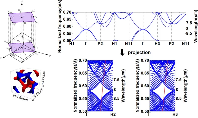
For experimental characterization, three-dimensional band structures are projected
onto a two-dimensional plane perpendicular to the crystal orientation, illustrated
in Figure 3.5. The projection plane is the purple rectangle, spanned by Γ-H2 and
Γ-H3, where the projection direction is illustrated by the red arrow. Projected band structures are convoluted along theΓ-H1, while the resolution is kept within the projection plane. To simulate projected band structures, we compute 3D band
structures, and superimpose them along the [001] (Γ-H1) direction. Figure 3.6 is the projected simulation of double gyroid band structures along the Γ-H2 and
Γ-H3 direction. The quadratic point degeneracy can be observed in both directions. Figure 3.7 is the projected simulation of Weyl points (parity breaking symmetry)
band structures along theΓ-H2 andΓ-H3 direction. The pair of Weyl points reside inside the plane spanned byΓ-H3 and Γ-N11. Therefore, after the [001] direction projection, two of the Weyl points could be observed along the Γ-H3 direction, close to the light line (red line). Figure 3.8 is the projected simulation of line
nodes (parity symmetry) band structures along theΓ-H2 andΓ-H3 direction, where similarly degenerate line nodes could be observed along theΓ-H3 direction.
3.4 Synthesis of double gyroid photonic crystals
To synthesize the three photonic crystals, we start by define the polymer scaffold
16
Figure 3.3: Band structures of double gyroids with unit cell size of 4.68µm (a) Double gyroids with quadratic point degeneracy (indicated by yellow circles) (b) Double gyroids with Parity breaking symmetry, which give rise to a pair of Weyl points. The Parity breaking airsphere is indicated by the yellow circle in the unit cell. Weyl points are indicated by the yellow circles along Γ-N11 and Γ-H3. (c) Double gyroids with two air spheres in one unit cell (indicated by yellow circles). Line nodes are indicated by yellow circlesΓ-N11 andΓ-H3.
Figure 3.4: Band structures of double gyroids with unit cell size of 4.68µm (a) Double gyroids with parity breaking symmetry by an airsphere, which give rise to a pair of Weyl points. The parity breaking airsphere is indicated by the yellow circle in the unit cell. Weyl points are indicated by the yellow circles along Γ-N11 and
Figure 3.5: Illustration of 3D band structure projection onto a 2D plane, along the Gamma-H1 direction.
18
Figure 3.7: Projection of Weyl points band structures along the [001] direction.
Figure 3.9: Synthesis of three-dimensional photonic crystals with high-refractive index materials.
coated with aluminum oxide or silicon dioxide by atomic layer deposition, shown in
Figure 3.9b. We then facilitate polymer removal by removing sides of the photonic
crystals with focused ion beam milling. After oxygen plasma cleaning, we obtain a
hollow oxide scaffold of the photonic crystal, shown in Figure 3.9c. The hollow oxide
scaffold is then conformally coated and in-filled with high refractive index material
such as a-Si via static chemical vapor deposition. Then cross sectional image of
the three-dimensional photonic crystal in Figure 3.9d consists of a-Si/Al2O3/a-Si.
Note that this method is also applicable for other high refractive index material.
For example, a-Ge can be deposited using the same method as a-Si. Other viable material candidate include TMDC material such as M oS2andW S2. For example,
M o2O3can be conformally deposited by ALD process, and then converted toM oS2
via sulfication.
3.5 Angle resolved mid-infrared spectroscopy
For initial optical characterization of double gyroids, we utilize FTIR, which is
illustrated in Figure 3.10a. Results of reflectance spectra from single gyroid (red),
double gyroids (blue) and double gyroids with parity breaking symmetry are shown
in Figure 3.10b. While we observe a reflectance peak from single gyroid
corre-sponding to the photonic bandgap, the reflectance peak decreases for double gyroid
20
reflectance and transmittance spectra from FTIR give us convoluted momentum
space information. In order to observe novel photonic states such as line nodes and Weyl points in double gyroid photonic crystals, I designed and built an optics set up
that can perform angle resolved spectroscopy with a quantum cascade laser, shown
in Figure 3.11. The set up consisted of a quantum cascade laser as the source, series
of ZnSe lenses to expand and refocus the laser beam into a 75µm diameter spot and
germanium beam splitter to direct 50% of the laser beam to the reference detector
and 50% to the sample. Two The sample and the pyroelectric detector are mounted
on top of concentric rotation stages to collect transmission and reflection at different
incidence angles. Alignment of the laser beam and the photonic crystal sample is
first performed by a visible CCD camera with a telescope lens. Then more precise alignment is performed by a magnifying lens and the magnified image is projected
onto a MCT camera. The angle of spread for beam focusing onto the sample is 80.
The wavefront of the beam is defined by:
E(r,z)= E0 ω0 ω(z)ex p(
−r2
ω(z)2)ex p(−i(k z+k r2
2R(z) −Φ(z))) (3.1)
where z is the axis of wave propagation, and R(z) is the radius of curvature of the
beam defined by:
R(z)= z(1+(zR z )
2)
(3.2)
At the focal point, z=0 kz=0, and R(z) approaches infinity, effectively we get a plane
wave wavefront.
The photonic crystal bandstructure is constructed from angle resolved reflectance
and transmittance spectra, all the way close to the light line. The set up is capable to
perform both normal incidence characterization, shown in Figure 3.12 and off
nor-mal incidence characterization, shown in Figure 3.13. To start off, we characterize
a double side polished silicon substrate, shown in Figure 3.14a and b. We observe clear Fabry-Perot resonance in both reflectance and transmittance characterization.
The reflectance characterization is also in agreement both in wavelength and
momen-tum compared to reflectance simulation shown in Figure 3.14c. Characterization
from double gyroids, oriented along [001] direction, reveals defect photonic states
emerging inside the bandgap. Measured bandstructures of double gyroids shown
in Figure 3.15b, are compared with simulated bandstructures projected based on
crystal orientation shown in Figure 3.15a. The double gyroid photonic crystal we
characterize here has a unit cell compression in the z direction by 70%. In this
Figure 3.10: FTIR characterization of double gyroids: (a) Illustration of FTIR set up (b) Reflectance spectrum from single gyroid (red), double gyroids (blue) and double gyroids with parity breaking symmetry (green) (c) SEM images of single gyroid (red), double gyroids (blue), and double gyroids with parity breaking symmetry (green)
taken into consideration for the simulation shown in Figure 3.15a. The
experimen-tal characterization has good correspondence at the degeneracy point compared to simulations.
Compared to FTIR, the characterization used here has selectively excite photonic
states at desired momentum and wavelength, providing more subtle information of
the bandstructures essential for characterizing defect states and surface states. To
resolve the subtlety of Weyl points, the degenerate energy states resulting from band
crossings of linear dispersion features in three-dimensional momentum space, such
characterization method is indispensable.
3.6 Conclusions and outlook
In summary, we aims to investigate topological phenomenon in 3D photonic crystals,
which is both a new platform to design high efficiency photonic devices and a playground for new physics. We have developed a synthesis method to fabricate
high refractive index three-dimensional photonic crystals, not limited to a-Si. To
characterize photonic states such as Weyl points in double gyroid photonic crystals,
we have constructed angle resolved transmission/reflection set up which enable us to
construct photonic bandstructures in the mid-infrared with momentum resolution.
22
Figure 3.11: Photo of angle resolved characterization set up
Figure 3.13: Angle resolved characterization set up for off normal incidence mea-surement
24
Figure 3.15: Double gyroid photonic band structures (a) simulation (b) experimental characterization
C h a p t e r 4
DIRAC-LIKE PLASMONS IN SILVER NANOPILLAR
HONEYCOMB LATTICES: DESIGN, FABRICATION AND
CATHODOLUMINESCENCE CHARACTERIZATION
Surface plasmons in honeycomb lattices of Ag nanoparticles exhibit Dirac-like
band structures, similar to the electronic band structure of graphene[37, 38]. Full
wave simulations for an infinite honeycomb lattice of silver nano-pillars reveal
hy-bridization of localized plasmonic modes between two neighboring pillars and the consequent formation of bonding and anti-bonding modes that are energetically
de-generate at Dirac points with a relative phase of Pi. Calculations also reveal that
distortion of the honeycomb lattice breaks the lattice inversion symmetry and opens
a photonic bandgap, whose width is proportional to the extent of distortion.
Further-more, electromagnetic simulations reveal the existence of Dirac-like plasmonic edge
states in finite width nanoribbons of the honeycomb nanoparticle lattice. Nanoscale
architecture of the honeycomb lattice may provide a new way to control directional
plasmon propagation by selective excitation of surface plasmon edge states without
backscattering.
Experimentally, we have utilized cathodoluminescence (CL) spectroscopy to study
angular emission patterns at various wavelengths and eventually construct band
structures of the silver pillars in honeycomb lattices. In a CL measurement, electron
beams are incident on the sample to excite plasmonic modes in the out of plane
di-rection, which is normally difficult to excite via optical measurement. The scattered
light due to the decay of surface plasmon excitations is collected by a parabolic
mirror and mapped to the momentum space, yielding a direct construction of band
structures in the Brillouin zone. In our initial CL measurement, we compared
angular emission patterns from a single silver pillar, silver pillar dimers and silver pillars in honeycomb lattices fabricated on a 15 nm thick free standing silicon nitride
membrane. The angular emission patterns from a single silver pillar exhibits strong
dipole radiation, while silver pillars in dimer have directional radiation resulting
from dipole interactions. For silver pillars in honeycomb lattices, we have observed
strong radiation patterns near the Brillouin zone edge, integrated over an interval of
![Figure 3.8: Projection of line nodes band structures along the [001] direction.](https://thumb-us.123doks.com/thumbv2/123dok_us/1121914.1141261/39.612.110.503.92.344/figure-projection-line-nodes-band-structures-direction.webp)