ISSN (Print) : 2347 - 6710
I
nternationalJ
ournal ofI
nnovativeR
esearch inS
cience,E
ngineering andT
echnology Volume 3, Special Issue 3, March 20142014 International Conference on Innovations in Engineering and Technology (ICIET’14)
On 21st & 22nd March Organized by
K.L.N. College of Engineering, Madurai, Tamil Nadu, India
ABSTRACT— In many pulse width modulated DC-DC
converter topologies, the controllable switches are operated in switch mode where they are required to turn the entire load current on and off during each switching cycle. Under these conditions, the switches are subjected to high switching stresses and power losses. Recently there is an increased interest in the use of resonant type DC-DC converters due to the advantages of high frequency of operation, high efficiency, small size, light weight, reduced Electro Magnetic Interference (EMI) and low component stresses.A novel PFC (Power Factor Corrected) Converter using Zeta DC-DC converter feeding a PMSM drive using a single voltage sensor is proposed for variable speed applications. A single phase supply followed by an uncontrolled bridge rectifier and a Zeta DC-DC converter is used to control the voltage of a DC link capacitor which is lying between the Zeta converter and a VSI (Voltage Source Inverter). The voltage of a dc-link capacitor of zeta converter is controlled to achieve the speed control of PMSM Drive. The zeta converter is working as a front end converter operating in DICM (Discontinuous Inductor Current Mode) and thus using a voltage follower. A sensor less control of PMSM is used to eliminate the requirement of Hall Effect position sensors. Using MATLAB/ Simulink 7.13 environment the model can be simulated to achieve a wide range of speed control with high power factor.
KEYWORDS— Adjustable Speed drives, DC-DC
Converter, PI Control, PMSM drive, Zeta Converter.
I. INTRODUCTION
M
odern electronic systems require high quality,[7] small, lightweight, reliable, and efficient power supplies. Linear power regulators, whose principle of operation is based on a voltage or current divider, are inefficient. They are limited to output voltages smaller than the input voltage.Also, their power density is low because they require low-frequency (50 or 60 Hz) line transformers and filters. Linear regulators can, however, provide a very high quality output voltage. Their main area of application is at low power levels as low drop-out voltage (LDO)regulators. Electronic devices in linear regulators operate in their active (linear) modes. At higher power levels, switching regulators are used. Switching regulators use power electronic semiconductor switches in on and off states. Since there is a small power loss in those states (low voltage across a switch in the on state, zero current through a switch in the off state), switchingregulators can achieve high energy conversion efficiencies. Modern power electronic switches can operate at high frequencies. The higher the operating frequency, the smaller and lighter the transformers, filter inductors, and capacitors. In addition, dynamic characteristics of converters improve with increasing operating frequencies.
The bandwidth of a control loop is usually determined by the corner frequency of the output filter. Therefore, high operating frequencies allow for achieving a faster dynamic response to rapid changes in the load current and/or the input voltage. High-frequency electronic power processors are used in dc–dc power conversion.
II.PROPOSEDSPEEDCONTROLSCHEMEOF
SENSORLESSPMSMDRIVE
The proposed scheme for the Sensor less PMSM drive fed by a Zeta based PFC converter operating in DICM mode is shown in Fig.2.1.The front end Zeta DC-DC converter maintains the DC link voltage to a set reference value. Switch of the Zeta converter is to be operated at high switching frequency for effective control and small size of components like inductors. A sensor less approach[12]is used to detect the rotor position for electronic commutation.A high frequency MOSFET of
Design of PFC Zeta Converter Fed Sensor
Less PMSM Drive Using
Pi Controller
Saravanan R #1, Chandrasekaran N*2 #
suitable rating is used in the front end converter for its high frequencyoperation whereas an IGBT’s (Insulated Gate Bipolar Transistor) are used in the VSI for low frequency operation.
The proposed scheme maintains high power factor and low THD[10] of the AC source current while controlling rotor speed equal to the set reference speed. A voltage follower approach is used for the control of Zeta DC-DC converter operating in DICM.
Fig.2.1. Proposed system block diagram The DC link voltage is controlled by a single voltage sensor. Vdc (sensed DC link voltage) is compared with Vdc* (reference voltage) to generate an errorsignal which is the difference of Vdc* and Vdc. The error signal is given to a PI (Proportional Integral) controller to give a controlled output. Finally, the controlled output is compared with the high frequency saw tooth signal to generate PWM (Pulse Width Modulation) pulse for the MOSFET of the Zeta converter.
III.PRINCIPLE OF OPERATION OF PROPOSED ZETA
CONVERTER
Vast majority of power converters used nowadays employ front-end diode bridge rectifiers. Such rectifiers draw pulsating currents which leave behind a great amount of harmonics, and considerably low power factor. For a single converter of this type used with a single-phase load such as in consumer electronic equipment, the problems may not seem serious. However, a great number of those equipment’s in parallel connection at a point of common coupling (PCC) to draw power simultaneously introduce some serious effects concerning reactive power and harmonic. The situations are quite common in offices and industries.
Fig.3.1 Isolated Zeta Converter
Several types of AC-DC converters have been introduced to achieve the demanded power conversion, and the fewer problems on harmonic and power factor. To name a few, these include the Cuk converter, [11]theSEPIC converter, the combined boost with double
winding fly back converter, and the zeta converter. Among those, the zeta converter, which is originally the buck-boost type, can be regarded as a fly back type when an isolated transformer is incorporated. An isolated zeta converter has some advantages including safety at the output side, and flexibility for output adjustment.
Fig.3.1 depicts the circuit diagrams of the isolated zeta converter such that its operation principle in the CCM could be readily explained. Fig.3.2 represents the 1st region of operation in which the switch S is “on”, and the diode D is “off”. This region takes the time from 0 to d1Ts seconds.
Fig.3.2 Ist Region of operation
The inductor Lm stores the energy received from the rectifier. The capacitor C1 supplies energy to the load (R) via the inductor Lo, and the capacitor Co. the currents through the inductors Lm and Lo increase linearly, while no current flows through the diode.
Fig.3.3 2nd Region of operation
Fig.3.3 represents the 2nd operation region in which the switch S is “off”, and the diode D is “on”. This region begins at the time d1Ts seconds, and ends by d2Ts seconds. The diode D is forward biased due to the voltage across the inductor Lm has reversed polarity, while the currents iLm and iLo decrease linearly. The stored energy in the inductor Lm is transferred to the capacitor C1. The load R receives energy from the inductor Lo. Hence, the current iD=iC1+iLo.
IV. STATE SPACE AVERAGED MODEL OF PROPOSED ZETA CONVERTER
(1-d1) Tsrespectively, the state equations in on switching cycle can be written as
x = As x + Bs u
y = Csx (1)
Where,
As = [A1d1 + A2 (1 – d1)] (2)
Bs = [B1d1 + B2 (1 – d1)] (3)
Cs = [C1d1 + C2 (1 – d1)] (4)
Linearization can be made to the above equations by considering small-signal perturbations such that
𝑥 = X + x ,y = Y + y , d1= D + x , u = U + u where X >>x , Y >>y , U >>u , D1>>D1be substituted into Eq. (1).
Under the steady-state condition of the state variables, the following equationscan be written as,
X = AavX + Bav U = 0; Y = CavX (5)
&
Aavx + [(A1+A2) X + (B1+B2) U]d + Bavu (6)
y +Cavx + [(C1-C2) X]d (7) Where,
Aav= A1D1 + A2 (1 – D1) (8)
Bav= B1D1 + B2 (1 – D1) (9)
Cav= C1D1 + C2 (1 – D1) (10)
From Eq. (2)
X = − Aav−1 BavU; Y
U= −Cav Aav −1
Bav (11)
Under small-signal assumption, taking the Laplace transform to Eq.(4) results in
x = [sI − Aav]−1[ BavVg(s) + [(A1− A2) X +
(B1− B2) Vg] d1(s)] (12)
y s + Cavx s + C1− C2 X d (s) (13)
Finally, the transfer functions can be obtained: forn Vg = 0
y (s)
d (s)1 = Cav [sI − Aav]
−1 (A
1− A2) X + (B1− B2) Vg +
C1−C2X (14)
And for d1= 0
y (s)
V (s)g = Cav [sI − Aav]
−1C av
(15)
VMATHEMATICAL MODEL OF THREE PHASE
VOLTAGE SOURCE INVERTER AND PMSM
1.Mathematical Model of Three Phase VSI
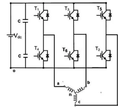
The PMSM armature winding is to be supplied from a 3 phase VSI whose power electronics devices (switches) would be switched according to the rotor position information for achieving VectorControl. The power circuit of a typical 3 phase, 2 level VSI [7] catering to a 3 phase armature winding of a 3 phase AC motor is shown in Fig.5.2 The inverter devices marked as T1 , T2 , T3 , T4 , T5 , T6 are to be switched to achieve Vector-Control as per a Sinusoidal Pulse Width Modulation (SPWM) strategy.
Fig5.1 Mathematical model of the 3 phase voltage source inverter
The mathematical model of the 3 phase VSI, as shown in Fig 5.1 as a block, should have the DC link voltage (Vdc ), the 3 switching functions (Boolean variables) Sa , Sb and Sc as input variables and should have the 3 phase voltages van , vbn and vcn as output variables. The output variables of the inverter will form as the input phase voltages to be fed to the PMSM armature winding (Star connected).
Voltages Vao, Vbo and Vco may be represented in terms of the switching functions as
Vao= VdcSa (16)
Vao= VdcSa (17)
Vao= VdcSa (18)
Where, Vao is the voltage of point `a' with respect to -ve DC link bus. Similar nomenclature is also applicable for other two phases. [7]The 3 phase voltage impressed on the star connected armature winding of PMSM (these are output voltage of the inverter) can be represent as,
Van = Vao - Vno (19)
Vbn = Vbo - Vno (20)
Vcn = Vco - Vno (21)
where Vno = The voltage of the neutral point `n' with respect to the point `o' of the DC bus. Van + Vbn + Vcn = Vao + Vbo + Vco – 3Vno assuming that the machine being balancedVan + Vbn + Vcn = 0. Hence inverter phase voltages can be expressed as,
Van = Vao−
Vao+ Vbo+ Vco
3
=2Vao− Vbo− Vco 3
Van =
2Sa−(Sb+SC)
3 (22)
Similarly,
Vbn =
2Sb− Sc+Sa
3 (23)
Vcn =
2Sc−(Sa+Sa)
3 (24)
II.Mathematical Model of PMSM:
The stator of the PMSM and the wound rotor synchronous motor (SM) with armature in stator are similar. In addition there is no difference between the backEMF produced by a permanent magnet in a PMSM [3]and that produced by an excited coil in a SM. Hence the mathematicalmodel of a PMSM is similar to that ofthe wound rotor SM. The rotor frame of reference is chosen because the PMSM three phase armature winding is fed from a 3 phase voltage source inverter (VSI), whichis switched in synchronism with the rotor position information of the PMSM.
Hence the frequency of the voltage or current in the PMSM armature winding atall instants is same as the electrical speed of the machine; electrical speed beingrelated to mechanical speed through the no. of poles of the machine. The following assumptions are madewhich deriving the D-Q model of the PMSM in rotor reference frame.[3]
1. Saturation is neglected. 2. The back EMF is sinusoidal.
3. Eddy currents and hysteresis losses are negligible.
Fig5.3 PMSM model block in D-Q reference frame, denoting input andoutput variables
The mathematical model is presented as a block in Fig. 5.3, where the three armature phase voltages (machine assumed to be star connected),[3] load torque parameters are input variables to the motor; and the armature current, electromagnetic torque, electrical speed, mechanical speed and rotor position are considered output variables. The rotor position is fed back as an input variable to the motor model.
VI. SIMULATION RESULTS &DISCUSSION OF A
PROPOSED ZETA CONVERTER
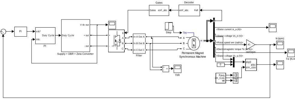
A PMSM system of 2300 rpm, 300 V, 14.3 N-m is taken for proposed speed control scheme using Zeta Converter. The proposed zeta converter has designed with the voltage output range from 0 to 500 V. A PI controller has used for voltage regulation and Speed Controller with proportionality and integral constant values of 0.013, 16.61 and 139.7290, 54.6363 respectively. The Proposed Scheme has implemented using MATLAB/SIMULINK shown in Fig 6.1& Fig 6.2.
Fig.6.1. SIMULINK model of proposed zeta converter
II .Simulation Results
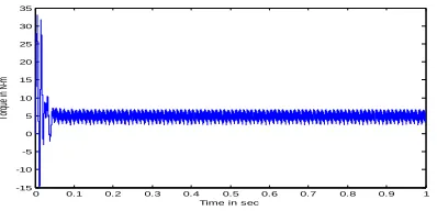
Fig. 6.3 shows the simulated speed response of PMSM with the set value of 2200 rpm and torque T= 5 N-m.The speed response obtained as the settling time less than 0.1s
4 - in 3 + in
2 - out
1 + out
g m
D S
Mosfet
Lo
1 2 D
Cf Cd
C1 1
Fig 6.3 Simulated Speed response of PMSM with set value of 2200 rpm, T=5 N-m
The simulated torque response of zeta converter fed PMSM with the set value of 2200 rpm and torque value can be obtained as T= 5 N-m can be shown in Fig.6.4The simulated rotor current response of zeta converter fed PMSM with the set value of 2200 rpm with T= 5 N-m can be shown in Fig.6.5
The simulated output voltage & inverter output voltage response of zeta converter fed PMSM with the set value of 2200 rpm with T= 5 N-m can be shown in Fig.6.6 & 6.7 respectively.
Fig 6.4 Simulated Torque response of PMSM with set value of 2200 rpm, T=5 N-m
Fig 6.6 Simulated output voltage response of Zeta converter with set value of 2200 rpm, T=5 N-m.
Fig 6.5 Simulated Rotor current of PMSM with set value of 2200 rpm, T=5 N-m
Fig 6.7 Simulated inverter voltage response with set value of 2200 rpm, T=5 N-m
0 0.1 0.2 0.3 0.4 0.5 0.6 0.7 0.8 0.9 1
-500 0 500 1000 1500 2000 2500 3000
Time in sec
Sp
ee
d
in
rp
m
0 0.1 0.2 0.3 0.4 0.5 0.6 0.7 0.8 0.9 1
-15 -10 -5 0 5 10 15 20 25 30 35
Time in sec
To
rq
ue
in
N
-m
0.3 0.35 0.4 0.45 0.5 0.55 0.6 0.65 0.7 0.75 0.8 -80
-60 -40 -20 0 20 40 60 80
Time in sec
C
u
rr
e
n
t
(I
rabc
)
in
A
m
p
s
0 0.1 0.2 0.3 0.4 0.5 0.6 0.7 0.8 0.9 1
0 50 100 150 200 250 300 350 400
Time in sec
Vo
lta
ge
(VDC
) i
n
vo
lts
0 0.1 0.2 0.3 0.4 0.5 0.6 0.7 0.8 0.9 1
-40 -30 -20 -10 0 10 20 30 40 50
Time in sec
V
ol
ta
ge
(Vab
) i
n
vo
Fig 6.2 MATLAB/Simulink model for PMSM Drive using Zeta Converter
VII.CONCLUSION
A simple control using a voltage follower approach has been used for voltage control and power factor correction of a PFC Zeta converter fed PMSM motor drive. A single stage PFC converter system has been designed and validated for the speed control with improved power quality at the AC mains for a wide range of speed. The performance of the proposed drive system has also been evaluated for varying input AC voltages and found satisfactory. The power quality indices for the speed control and supply voltage variation have been obtained within the limits by International power quality standard IEC 61000-3-2.The proposed drive system can be used in various adjustable speed drives for many low power applications.
REFERENCES
[1] Limits for Harmonic Current Emissions (Equipment input current”16 A per phase), International Standard IEC 61000-3-2, 2000.
[2] B. Singh, B. N. Singh, A. Chandra, K. Al-Haddad, A. Pandey and [3] D.P. Kothari, “A review of single-phase improved power quality AC-DC converters,” IEEE Transactions on Industrial Electronics, vol. 50, no. 5, pp. 962– 981, Oct. 2003.
[4] T. Kenjo and S. Nagamori, Permanent Magnet Brushless DC Motors, Clarendon Press, Oxford, 1985.
[5] T. J Sokira and W. Jaffe, Brushless DC Motors: Electronic Commutation and Control, Tab Books, USA, 1989
[6] J. R. Handershot and T.J.E Miller, Design of Brushless Permanent Magnet Motors, Clarendon Press, Oxford, 1994 [7] J. F. Gieras and M. Wing, Permanent Magnet Motor Technology
Design and Application, Marcel Dekker Inc., New York, 2002 [8] N. Mohan, T. M. Undeland and W. P. Robbins, Power
Electronics: Converters, Applications and Design, John Wiley and Sons Inc, USA, 1995.
[9] A. Peres, D. C. Martins and I. Barobo, “Zeta Converter Applied in Power Factor Correction”, in Proc. IEEE PESC’94, 1994, pp.1152-1157.
[10] S. Singh and B. Singh, "Voltage controlled PFC Zeta converter based BLDC MOTOR drive for an air-conditioner," 2010 International Conference on Industrial and Information Systems (ICIIS), pp.550-555, 29th July 2010- 1st Aug. 2010.
[11] Bhim Singh, B.P.Singh and SanjeetDwivedi, “AC-DC Zeta Converter for Power Quality Improvement of Direct Torque Controlled PMSM Drive”, Korean Journal of Power Electronics, Vol. 6, No. 2, pp.146-162, April 2006.
[12] J. Uceeda, J. Sebastian and F.S. Dos Reis, “Power Factor Preregulators Employing the Flyback and Zeta Converters in FM Mode” in Proceedings of IEEE CIEP’96, 1996, pp.132-137. [13] D.C. Martins, “Zeta Converter Operating in Continuous Conduction Mode Using the Unity Power Factor Technique”, in Proceedings of IEE PEVSD’96, 1996, pp.7-11.
[14] Paul P. Acarnley and John F. Watson, “Review of Position-Sensorless Operation of Brushless Permanent-Magnet Machines”, IEEE Transactions on Industrial Electronics, Vol. 53, no. 2, April 2006.
[15] James P. Johnson, M. Ehsani and YilcanGuzelgunler, “Review of Sensorless Methods for Brushless DC” Industry Applications Conference, 34th IAS Annual Meeting, 1999, Vol. 1, pp. 143-150.
[16] F. Wu, S. A. Ljang and Y. M. Chen, “Design Optimization for Asymmetrical ZVS-PWM Zeta Converter”, IEEE Trans. on Aerospace and Electronic Systems vol. 39, no.2, pp. 521-532, April 2003.
[17] M.H. Rashid, Power Electronics: Circuits, Devices and
Applications (3rd edition.). Pearson-Prentice Hall, pp.186-203,
2004.
[18] E. Vuthchhay, C. Bunlaksananusorn, and H. Hirata, “Dynamic modeling and control of a zeta converter,” International Symposium, Communications and Information Technologies,
ISCIT. pp.498-503, 2008
[19] C. Sudhakarababu, and M. Veerachary, “Zeta converter for power factor correction and voltage regulation,” IEEE Region 10
Conference, TENCON, vol.4, pp.61-64, 2004
[20] D. Cismasiu, V. Popescu, and D. Lascu, “Single-stage PFC power supply with universal input and automatic voltage clamping,” 11th WSEAS International Conference on Circuits, pp. 109-114, 2007.
[21] E. Niculescu, D-M. Purcaru, and M.C. Niculescu, “A steady-state analysis of PWM Sepic converter,” 10th WSEAS
International Conference on Circuits, pp. 217-222, 2006.
[22] E. Niculescu, M.C. Niculescu, and D-M. Purcaru, “Modeling the PWM Sepic converter in discontinuous conduction mode,” 11th
WSEAS International Conference on Circuits, pp. 98-103, 2007.
[23] C. Wu, “Evaluation and implementation of the optimum magnetic design of the Cuk converter in comparison to the conventional buck-boost converter,” IEEE Trans.Magnetics,
vol.18, pp.1728-1730, 1982.
[24] J.J. Jozwik, and M.K. Kazimierczuk, “Dual sepic PWM switching-mode DC/DC power converter,” IEEE Trans.
Industrial Electronics, vol.36, pp.64-70, 1986.
[25] D.C. Martins, and A.H. de Oliveira, “Isolated three-phase rectifier using a Sepic DC-DC converter in continuous conduction mode for power factor correction,” WSEAS Trans
Circuits, vol. 2, no. 1, pp. 13-19, 2003
Reference
speed (RPM)
-K-rad2rpm
Discrete, Ts = 5e-006 s.
PI dq0 sin_cosabc v + -Vdc Vab g A B C + -Timer Te (N.m)
Duty Cy cle V dc out
+ out
- out
Supply + DBR + Zeta Converter
Step m A B C Tm Permanent Magnet Synchronous Machine v dc* Vdc Duty Cy cle
PI N (rpm) emf _abc Gates Gates In A In B In C Out A Out B Out C Filter Freq Sin_Cos wt Hall emf _abc Decoder 2200 0
<Stator current is_a (A)>
<Stator v oltage Vs_d (V)>
<Rotor speed wm (rad/s)>
<Electromagnetic torque Te (N*m)>
BIOGRAPHY
Saravanan R has obtained his B.E degree
in Electrical and Electronics Engineering from Anna University, Chennai in the year 2010 and Pursuing his M.E., degree (Part Time) in Power Electronics and Drives Engineering from Anna University Chennai, during the year 2011- 2014. He has published 1 paper in both National Conferences and International Conference. He has also published 2 papers in International journals. His areas of interest include Power Electronics, Control of Drives, Control systems and Electrical Machines. He has 3 years of teaching experience. Currently he is working as a Lecturer in the department of Electrical and Electronics Engineering at PSNA College of Engineering and technology, Dindigul, Tamil Nadu, India.
Chandrasekaran N has obtained his B.E
degree from Bharathiar University, in the year 1998 and M.E., degree from Anna University Chennai, in the year 2004. He has secured first rank in M.E and got gold