2
density. I. Two-step remote plasma-assisted
oxidation-deposition process
Choelhwyi Bae and Gerald Lucovskya)
Departments of Physics, Materials Science and Engineering, and Electrical and Computer Engineering, North Carolina State University, Raleigh, North Carolina 27695-8202
(Received 17 June 2004; accepted 23 August 2004; published 20 October 2004)
In previous studies, device-quality Si-SiO2interfaces and dielectric bulk films共SiO2兲were prepared using a two-step process: (i) remote plasma-assisted oxidation (RPAO) to form a superficially interfacial oxide共⬃0.6 nm兲and(ii)remote plasma-enhanced chemical vapor deposition(RPECVD) to deposit the oxide film. The same approach has been applied to the GaN-SiO2system. Without an RPAO step, subcutaneous oxidation of GaN takes place during RPECVD deposition of SiO2, and on-line Auger electron spectroscopy indicates a⬃0.7-nm subcutaneous oxide. The quality of the interface and dielectric layer with/without RPAO process has been investigated by fabricated GaN metal-oxide-semiconductor capacitors. Compared to single-step SiO2 deposition, significantly reduced defect state densities are obtained at the GaN-SiO2 interface by independent control of GaN-GaOx interface formation by RPAO and SiO2 deposition by RPECVD. © 2004 American
Vacuum Society.[DOI: 10.1116/1.1807396]
I. INTRODUCTION
GaN has emerged as an important material for optoelec-tronic and high-temperature/high-power/high-frequency de-vice applications. As such, GaN-dielectric insulators for gate dielectrics1and surface passivation layers2have become im-portant issues in device processing. Studies of GaN metal-insulator-semiconductor (MIS) systems have focused on re-ducing fixed-oxide charge and interface-trapped charge. For
n-type GaN MIS systems, interface state density共Dit兲 in the range of low-to-mid 1011cm−2eV−1 has been obtained with-out in situ native oxide removal and thin intermediate layer (or sacrificial layer) preparation.1 These results are remark-ably different from the other compound semiconductors, where surface passivation has been an important issue to avoid thin native oxide formation between deposited oxide and substrate. Considering the deep depletion without severe Fermi-level pinning, and the low Dit of n-type GaN MIS systems, the native oxide of GaN is exempt from the criti-cally undesirable factors such as multiple-type oxides, ther-modynamic instability, metallic residue, and smaller band gap than that of the semiconductor. In the cases of GaAs metal-oxide-semiconductor (MOS) systems, improved sur-face passivation was initially obtained by removal of As2O3 and subsequent formation of a few monolayers of Ga2O3film or 共Ga2O3兲1−x共Gd2O3兲x.
3–5
The main difference of GaN from other III-V semicon-ductors, such as GaAs and GaP, is the volatility of N oxide species, e.g., NO and N2O. This suggests that a thin native oxide of GaN can be used to control the semiconductor-deposited dielectric interface. The purpose of our present work is to investigate how a controlled superficially thin
na-tive oxide of GaN can improve the quality of the interface and dielectric layer of the GaN MOS system. For the oxide film deposition by a plasma-assisted process, ex situ wet chemical and in situ removal of the air-grown native oxide does not guarantee that there is no interfacial oxide because the presence of oxidant and excitation very often leads to the growth of an oxide on the substrate surface. When SiO2thin films were deposited on Si, Ge, GaAs, and CdTe using remote plasma-enhanced chemical vapor deposition (RPECVD), the substrates were slightly consumed by plasma-activated species that diffused though the deposited oxide layer and oxidized the underlying substrate.6–8These parasitic reactions, or subcutaneous oxidation, during oxide film deposition by the RPECVD process degrade the electri-cal characteristics of the interface. To prevent the subcutane-ous oxidation of the GaAs and Ge, a thin sacrificial Si layer was deposited before the deposition of the SiO2thin film.6–8 To prepare a device-quality Si-SiO2 interface and dielectric bulk film 共SiO2兲, the superficially thin oxide layer
共⬃0.6 nm兲 is formed on the silicon substrate by a remote plasma-assisted oxidation (RPAO)process, and the remain-der of the oxide layer is deposited by a RPECVD process.9 After formation of⬃0.6 nm of oxide in⬃15 s, the oxidation rate slows down to ⬃0.3– 0.4 nm/ min. Therefore, during plasma-enhanced deposition at rates of ⬃2.5– 5 nm/ min, plasma-activated O species are consumed faster by deposi-tion reacdeposi-tions with SiH4 than by continued oxidation at the buried Si-SiO2 interface.
10
The same RPAO-RPECVD pro-cess has been applied to SiC,11 Ge,12 and GaN13 and has yielded a semiconductor-dielectric interface with reduced net oxide charges compared with the direct deposition of SiO2 film on a semiconductor substrate.
On the other hand, the low Ditof GaN MIS systems also contributed to the possible underestimation of the actual Dit. In a wide-band-gap semiconductor, the Terman method at
a)Author to whom correspondence should be addressed; electronic mail:
the gate voltage axis as interface trap occupancy changes with gate bias.15,16In the estimation of Ditusing the Terman method, it is well known that doping concentration should be known exactly to compare the difference between the mea-sured and calculated C-V curves. However, doping concen-tration for calculated C-V curves has been selected until a close fit of C-V curves was obtained over the entire voltage range because the C-V characteristics of GaN MOS capaci-tors showed deep depletion instead of inversion. Then, the
C-V curve “stretch” associated with uniformly distributed Dit could be misinterpreted as an increased doping concentra-tion, and can lead to the underestimation of Dit. The high-low frequency method or conductance method, which does not require a theoretical curve to compare with the measured curve, can be considered to reduce the uncertainty associated with doping concentration in C-V characterizations of the GaN MOS system. However, due to high series resistance
共Rs兲 and system noise, a quasistatic or low (below 100 Hz) frequency C-V curve has not been reported, and the conduc-tance method has been used on occasion for GaN MOS analysis. In addition, there are side contact effects on the capacitance properties17for the MOS system using thin epi-taxial layers grown on insulating substrates. For the GaN MOS structures, it is also difficult to properly extract the oxide-fixed charge from the flat-band voltage shift 共⌬Vfb兲. The extraction of the fixed charge from ⌬Vfb has several uncertainties, such as the (i) compensated effect14 among several types of charge, (ii) uncertain doping concentration of GaN MOS system, which was usually obtained from a close fit of the C-V curve, and (iii) assumption of both the electron affinity of GaN and work function of the Al gate as 4.1 eV.
In this work, the occurrence of subcutaneous oxidation of GaN during plasma-enhanced deposition of SiO2 films has been studied using Auger electron spectroscopy(AES) mea-surements. The quality of the interface and dielectric layer with/without RPAO process was investigated by fabricated GaN MOS capacitors.
II. EXPERIMENT
The epitaxial GaN(0001)layer was grown directly on the
c plane of sapphire by hydride vapor-phase epitaxy (
Tech-nologies Devices International, Inc.). Silicon was used as
n-type dopant, and the thickness of the GaN epitaxial layer
GaN sample was exposed to reactive species from a remote N2/ He discharge at 0.02 Torr to reduce residual contami-nants after wet-chemical treatments.18 Superficially thin GaOx
共⬃1 nm兲, with a composition close to Ga2O3or x⬃1.5, was formed by the RPAO process at 0.3 Torr using O2source,
18
and a thin SiO2film was deposited by the RPECVD process at 0.3 Torr.10 The substrate temperature was 300 ° C, and plasma power was 30 W at 13.56 MHz. The experimental procedure was to alternate AES measurements with the SiO2 deposition for 20 s, i.e., interrupted processing and AES analysis cycles.
For the fabrication of GaN MOS capacitors, SiO2 films were deposited onto wet-chemical-treated GaN samples with/without RPAO. After gate dielectric insulator deposi-tion, the sample was rapid-thermal annealed at⬃900 ° C for 30 s in Ar atmosphere. A 300-nm-thick Al layer was evapo-rated and defined by the conventional lithography process. For GaN MOS capacitors without RPAO, postmetallization annealing (PMA) was performed at 400 ° C for 30 min in forming gas共N2/ H2兲. The electrical properties of GaN MOS capacitors were investigated using an HP 4284A (precision inductance-capacitance-resistance meter). The area of the de-vice being tested was 4⫻10−4cm2.
III. RESULTS AND DISCUSSION
A. Subcutaneous oxidation of GaN during deposition of SiO2
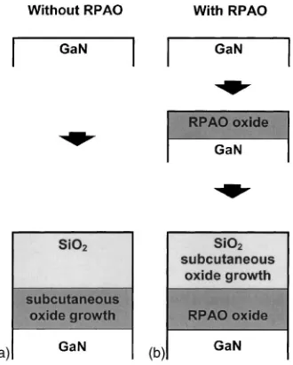
To demonstrate subcutaneous oxidation of GaN during deposition of SiO2, two different process sequences, shown in Fig. 1, were used:(a)a direct deposition of SiO2on GaN using the RPECVD process and(b)a two-step process, i.e., RPAO process to form a superficially thin RPAO oxide layer 共⬃1.0 nm兲, or GaOx with x⬃1.5,
18
and deposition of SiO2on GaN using the RPECVD process. Figure 2 displays differential AES spectra for (i) the in situ
Ga共LMM兲 共⬃1061 eV兲 features mainly associated with Ga–N bonding in the GaN substrate decreased in strength, whereas the O KLL 共⬃506 eV兲 feature mainly associated with O–Si bonding in the deposited oxide layer increased. Figure 3 displays differential AES spectra for (i)the RPAO process of the GaN sample using O2source gas, followed by (ii)–(vi) the SiO2 deposition on the GaN sample for 20– 160 s. Note that the N KLL features of both samples in
Figs. 2 and 3 disappeared at nearly the same SiO2deposition time, 120 s. In addition, the Ga LMM features of both samples show similar intensity after the deposition of SiO2 for 160 s. This indicates that oxide thickness 共tox兲 of both samples became similar after the deposition of SiO2film for 120 s.
Figure 4 shows a comparison of determined tox of GaN samples shown in Figs. 2 and 3 as a function of SiO2 depo-sition time. Assuming the negligible dependence of electron escape depth on oxide overlayer, i.e., GaOx or SiO2, oxide thickness 共tox兲 is obtained from (Ref. 18 and references therein):
FIG. 1. Two different process sequences were used to demonstrate the pres-ence of subcutaneous oxidation of GaN during deposition of SiO2:(a)direct deposition of SiO2on GaN using RPECVD process and(b)two-step pro-cess, i.e., RPAO process to form a superficially thin RPAO oxide layer 共⬃1.0 nm兲, or GaOxwith x⬃1.5 and deposition of SiO2 on GaN using RPECVD process.
FIG. 2. Differential AES spectra for(i)in situ N2/ He-plasma-cleaned GaN sample followed by(ii)–(vi)SiO2deposition on GaN sample for 20– 160 s. Initial oxide thickness共tox兲prior to SiO2film deposition on GaN sample was below 0.1 nm.
FIG. 3. Differential AES spectra for(i)RPAO process of GaN sample using O2 source gas followed by(ii)–(vi) SiO2deposition on GaN sample for 20– 160 s. Initial oxide thickness共tox兲prior to SiO2film deposition on GaN sample was⬃1.0 nm.
tox=ln
冉
1 + IoNIoO⫻ Io
IN
冊
, 共1兲
where IN= N KLL Auger electron intensity from the GaN substrate, IoN= N KLL Auger electron intensity from the clean GaN substrate, IO= O KLL Auger electron intensity from the thin GaOxlayer, IoO= O KLL Auger electron inten-sity from the thick GaOxlayer, and= electron escape depth
for O and N,⬃1 nm.
The difference of tox between two samples was gradually reduced by increasing SiO2 deposition time from the initial value of⬃1 nm, and saturated to ⬃0.3 nm. This reduction indicates that ⬃0.7 nm of GaOxwas formed during the
di-rect SiO2deposition on the GaN sample without RPAO due to the subcutaneous oxidation process. The nearly linear SiO2 deposition rate of the sample with RPAO means that negligible subcutaneous oxidation occurred, and⬃1.0 nm of GaOxusing the RPAO process (or several monolayers of a
sacrificial Si)can inhibit the subcutaneous oxidation process of GaN during the SiO2deposition.
Figure 5 displays the peak shift of nondifferentiated AES spectra by the SiO2deposition for(ii)20,(iii)40,(iv)60,(v) 80, and(vi)180 s on GaN samples(a)without RPAO and(b) with RPAO. The nondifferentiated AES spectrum of a thick GaOxsample, obtained by remote O2/ He plasma oxidation of the GaN sample for 30 min, is included as a reference in Fig. 5(b). The AES O KLL feature at⬃505.5 eV of the GaN sample with RPAO, shown in Fig. 5(b), gradually shifts to lower energy as the SiO2 deposition time increased. This gradual peak shift 共⬃4 eV兲 of the O KLL feature indicates that O-Ga bonds change to O-Si bonds. For the direct depo-sition of SiO2 on a cleaned GaN sample without RPAO, shown in Fig. 5(a), the O KLL feature after the deposition of SiO2for 20 s was located⬃1.5 eV higher position than that of thick SiO2films共⬎3 nm兲 and gradually shifted to lower energy as the SiO2deposition time increased. This peak shift
demonstrates that thin GaOx, or subcutaneous oxide, was
formed during the direct SiO2deposition on the GaN sample.
B. GaN MOS system with/without RPAO
The quality of the interface and dielectric layer(i)without and(ii)with the RPAO process was compared by the fabri-cated GaN MOS capacitors. The RPAO process was per-formed for 30 s to form the RPAO oxide of⬃1.0-nm thick-ness, and the RPECVD process was performed for 12 min to deposit SiO2of⬃40-nm thickness. Note that both MOS ca-pacitors(i)without RPAO and(ii)with RPAO have an inter-facial GaOxlayer below the SiO2film because subcutaneous oxide 共⬃0.7 nm兲 was formed at the sample without RPAO. In this section, we discuss a significant role of(i) subcutane-ous oxide and(ii)RPAO oxide in determining the electrical properties of the semiconductor/oxide interface. Compared to the MOS sample with RPAO, the sample without RPAO showed a large ⌬Vfb to the positive voltage direction and frequency dependence in the depletion region. Postmetalliza-tion annealing(PMA)was performed for the sample without RPAO at 400 ° C for 30 min in forming gas共N2/ H2兲, as well as for all of the samples with the RPAO step.
We measured conductance-voltage 共G-V兲 characteristics of GaN MOS capacitors(i)without RPAO before/after PMA and (ii) with RPAO before PMA at room temperature and 1 MHz. Figure 6 displays the measured G-V curves that have clear peaks of interface trap reduction. The value of Rs
de-termined from measured capacitance and conductance in ac-cumulation was⬃50– 70⍀. This relatively low value of Rs
for the GaN MOS system is attributed to thick
共⬃5-m兲 GaN epilayer with high doping concentration
共⬃5 – 10⫻1017cm−3兲. The low and symmetric base line of the G-V curve indicates that there are no significant trapping effects and charge injection into the superficially thin RPAO oxide. For the electron-beam-deposited Ga2O3 film, where the Ga2O3was used as a bulk oxide of the MOS system,
19,20
interface trap loss is masked by high oxide loss. The conduc-tance peak heights of samples (i) without RPAO before
FIG. 5. Peak shift of nondifferentiated AES spectra by the SiO2deposition for (ii) 20,(iii) 40,(iv)60, (v) 80, and(vi)180 s on GaN samples (a) without RPAO and(b)with RPAO.
PMA, (ii) without RPAO after PMA, and (iii) with RPAO before PMA were ⬃2.4, 1.5, and 0.5S, respectively. Be-cause these samples have nearly similar values of Rs and
oxide capacitance共Cox兲, Ditof each sample will be approxi-mately proportional to the measured conductance peak heights.
To estimate the distribution of Dit using the Terman method, C-V curves of each sample were measured at room temperature and 1 MHz. In the evaluation of expressions for theoretical C-V curves,15,16 the same fundamental constants as in a previous paper21 were used. The relative dielectric constant of GaN is taken as 9.5. The intrinsic carrier concen-tration共ni兲is 2.0⫻10−10cm−3for GaN at room temperature.
Both the electron affinity of GaN and the work function of the Al gate are assumed as 4.1 eV. Figure 7 shows the mea-sured and calculated C-V curves of the GaN MOS capacitor with RPAO. Also shown is the measured conductance. The calculated C-V curve was obtained using a net donor concen-tration 共ND兲 of 1.7⫻1018cm−3 and fixed oxide charge of
3.5⫻1011cm−2(or ⌬Vfbof −0.6 V). These values were de-termined from a close fit of the measured C-V curve over the entire voltage range. The measured C-V curve shows a small deviation from the calculated C-V curve between −1 and −7 V. Note that this deviation cannot be attributed to inter-face states because the measured curve is sharpened, rather than stretched. Figure 8 displays the 1 / C2-V characteristics. Two linear lines fit the characteristics, and NDobtained from
the slope increased from the initial value of 1.5
⫻1018cm−3 to 1.7⫻1018cm−3. It is not clear whether this result is caused by the actual change in NDor by voltage and capacitance changes associated with interface states. Figure 9 shows the distribution of Ditby applying the Terman method. The minimum Dit was estimated as⬃1⫻1011cm−2eV−1at
⬃0.45 eV below the conduction band edge. For the sample without RPAO before/after PMA, as shown in Fig. 10, there was a reduction of the stretch-out in the measured C-V curves. When the measured C-V curves were partially fit above ⬃30 pF, measured curves agreed with calculated curves. NDwas 2.7⫻1018cm−3 for the sample before PMA
and 2.0⫻1018 cm−3for the sample after PMA. These results indicate that the C-V curve stretch-out along the gate voltage axis, which is associated with interface trap occupancy changes, can sometimes be misinterpreted as an increased value of ND.
FIG. 7. Calculated and measured C-V curve of the GaN capacitor with RPAO at room temperature and 1 MHz. Also shown is the measured conductance.
FIG. 8. 1 / C2characteristics as a function of gate voltage. Net doping con-centration 共ND兲 obtained from the slope was 1.5⫻1018 and 1.7
⫻1018cm−3.
FIG. 9. Distribution of the density of interface state 共Dit兲 of GaN MOS capacitor with RPAO using Terman method.
Because the high-low frequency method does not require a theoretical curve to compare with the measured curve, this method can reduce the uncertainty of the extraction of Dit associated with doping concentration. In this study, C-V curves measured at 1 MHz and 3 kHz were used as high-and low-frequency C-V curves, respectively. The actual Dit will be higher than the estimated value using this method because the 3-kHz frequency is not sufficiently low that slow interface traps respond. In addition, the gate voltage where low and high C-V curves showed the maximum capacitance difference 共⌬Cmax兲can be used to estimate the energy level of the traps contributing to Dit. The capacitance difference between low and high frequency is due to the electron emis-sion and capture by interface states. If each energy level has the same values of Dit and time constant of electron emis-sion, the capacitance difference will be continuously in-creased with gate bias sweep from accumulation to deple-tion. In fact, the capacitance difference showed a maximum value and gradually decreased to a negligible value because the time constant for electron emission from interface states increased exponentially with energy from the conduction band edge. Then, a limiting energy where Ditcan be inves-tigated without underestimation will be obtained at the gate voltage of ⌬Cmax. Figure 11 shows the frequency depen-dence共1 kHz to 1 MHz兲of the C-V characteristics of GaN MOS capacitors (i)without RPAO after PMA and (ii) with RPAO. The gate voltage was swept from positive to negative voltage at room temperature. Figure 12 shows the distribu-tion of Ditas a function of gate voltage calculated from
15,16
Dit=
Cox
q
冉
Clf/Cox
1 − Clf/Cox
− Chf/Cox 1 − Chf/Cox
冊
, 共2兲
where Clf is the capacitance measured at low frequency (or 3 kHz) and Chf is the capacitance measured at high fre-quency (or 1 MHz). The minimum value of Dit was deter-mined at the gate voltage where low and high C-V curves showed ⌬Cmax. For the C-V curves measured at 1 MHz, shown in Fig. 11, the values of C / Cox at the voltage of
⌬Cmaxwere⬃0.88– 0.89. This small difference in the values
of C / Coxindicates that the minimum Ditwas determined at the similar energy level. The minimum value of Dit(i) with-out the RPAO was ⬃4⫻1012cm−2eV−1 at −2.5 V, and(ii) with RPAO was ⬃7⫻1011cm−2eV−1 at −4.1 V. Figure 13 shows the distribution of Ditover the band-gap energy near the conduction band edge using the Terman method and the high-low frequency method. When the extracted values of
Ditwere compared at⬃0.3 eV, where⌬Cmaxwas observed,
Dit using the Terman method is⬃2 times smaller than that using the high-low frequency method. Note that the calcu-lated curve without Ditwas obtained using NDfrom a close fit of the C-V curve, and the actual energy level for minimum
Ditwas located at a level deeper than⬃0.3 eV.
The conductance method was also used to clarify the es-timated Ditusing the high-low frequency method. Figures 14 and 15 show the parallel conductance loss 共Gp/兲 versus
angular frequency 共兲 curves at selected gate voltages. As-suming negligible series resistance, Gp/ was obtained from16
FIG. 11. Frequency dependence共1 kHz to 1 MHz兲of the C-V characteris-tics of GaN MOS capacitors (i) without RPAO after PMA and(ii)with RPAO.
FIG. 12. Density of interface state共Dit兲of GaN MOS capacitors(i)without RPAO and(ii)with RPAO using the high-low frequency method. The mini-mum Ditwas determined at the gate voltage where low and high C-V curves showed the maximum capacitance difference共⌬Cmax兲. Then, minimum Dit of(i)without and(ii)with RPAO was⬃4⫻1012cm−2eV−1at −2.5 V and ⬃7⫻1011cm−2eV−1at −4.1 V, respectively.
Gp
=
GmCox2 Gm2+2共Cox− Cm兲2
, 共3兲
where Gmis the measured conductance and Cmis the
mea-sured capacitance. From the graphically determined standard deviation of band bending共s兲and universal function共fD兲as
a function ofs, Ditof each sample was calculated from 16
Dit=
冉
Gp
冊
fp关qfD共s兲兴−1, 共4兲
where fpis the frequency corresponding to the peak value of
Gp/. The determined values of fDwere about 0.34–0.38 for
the sample without RPAO and 0.24–0.26 for the sample with RPAO. Figure 16 shows Ditfrom the conductance measure-ments in Figs. 14 and 15, along with Ditfrom the high-low frequency method in Fig. 12. Both methods indicate well that
Ditof(i)without RPAO after PMA is⬃5 times larger com-pared to that of(ii)with RPAO. Therefore, it is clear that the two-step (RPAO-RPECVD) process can effectively reduce
Ditof the GaN MOS system.
C. High-temperature and photo-assistedC-V measurements
The high-temperature C-V method22–24and photoassisted
C-V method21,22,25 have been used to estimate Dit over a
significant portion of the wide band gap. The GaN MOS sample with RPAO was investigated using these two meth-ods.
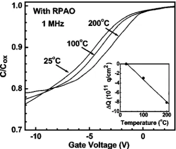
Figure 17 shows the C-V characteristics measured at 25° – 200 ° C in the dark. Also shown is the change in polar-ization charge共⌬Q兲(Ref. 23)by increasing temperature. As reported by Matocha, Chow, and Coutmann,23 our C-V curves also showed a positive shift with increasing tempera-ture. They reported that their large positive shift共⬃2 V兲was caused by the pyroelectric polarization of GaN because the change in the semiconductor bulk potential 共Ec-Ef兲 and
in-terface trap charge 共Qit兲 with increasing temperature make
⌬Vfb(below 0.1 V)negligible in the negative-voltage direc-tion. For the capacitor with RPAO, shown in Fig. 17, calcu-lated⌬Vfbfrom the change in Ec-Efwas about −0.06 V with
increasing temperature from 25° to 200 ° C. The deter-mined pyroelectric charge coefficient was ⬃4.9
⫻109q / cm2K. As shown in Fig. 17, however, C-V curves
FIG. 14. Parallel conductance loss共Gp/兲vs angular frequency共兲curves
measured at 25 ° C for GaN MOS capacitor without RPAO after PMA. The graphically determined standard deviation of band bending共s兲was 0.5–0.9
(in the unit of kT/q).
FIG. 15. Parallel conductance loss共Gp/兲vs angular frequency共兲curves
measured at 25 ° C for GaN MOS capacitor with RPAO. The graphically determined standard deviation of band bending共s兲was 1.7–1.9(in the unit
of kT/q).
FIG. 16. Density of interface state共Dit兲of GaN MOS capacitors(i)without RPAO after PMA and(ii)with RPAO using the conductance method and the high-low frequency method.
were stretched along the voltage axis and flatten with in-creasing temperature. This indicates that electron-capture/ emission-associated interface traps increased at high tem-perature and were not negligible in the measured positive shift of Vfb.
Figure 18 shows the photoassisted C-V characteristics measured at room temperature. The sweep rate of gate bias was 100 mV/ s. From ND of 1.7⫻1018cm−3, the threshold voltage was determined as about −18 V. The bias first swept from accumulation共+3 V兲 to deep depletion共−21 V兲in the dark. While the bias remained at −21 V, the sample was illuminated by ultraviolet lamp共365 nm兲 until the measured capacitance saturated. After the capacitance saturated, the lamp was turned off and the bias was swept back to accumu-lation in the dark. Due to the higher photosaturated capaci-tance 共⬃31 pF兲 than the expected inversion capacitance
共⬃25 pF兲, “interface state ledge”14,26,27 was not observed, and photoinduced hysteresis 共⌬Vp兲 was obtained within the limited voltage range. Tungsten-bulb or microscope illumi-nation can produce the same value of photosaturated capaci-tance with a reduced ⌬Vp. The discrepancy between photo-saturated capacitance and the expected inversion capacitance was also reported,21,22 and was attributed to the small minority-carrier recombination rate, rather than to charge transfer from interface states.22 In this study, the photosatu-rated capacitance was quite similar to the satuphotosatu-rated capaci-tance measured at 200 ° C, as well as that of MOS samples without RPAO.
Details of high-temperature C-V and photoassisted C-V will be discussed in a separate paper. It would be interesting to investigate the high-temperature C-V characteristics of nonpolar(or Ga- and N-terminated surface)GaN MOS struc-tures as well as the photoassisted C-V characteristics by varying the gate-voltage sweep rate, and this will be pre-sented in a separate paper.
IV. CONCLUSION
A low-temperature RPAO process for interface formation and passivation has been extended from Si and SiC to GaN. The process provides the control of ultra-thin interfacial
lay-2
minimize RPAO oxide thickness as a superficially thin
共⬃0.6– 1.0-nm兲oxide, followed by a remote plasma-assisted interface nitridation step that introduces approximately one monolayer of nitrogen atoms at the GaN-gallium oxide inter-face. Also, a post-oxide-deposition anneal and forming-gas anneal need to be investigated to obtain optimized process-ing conditions.
The remote plasma processing can be extended to the fol-lowing applications:(i)the gate dielectric insulator of a GaN MOS field-effect transistor, (ii) the passivation layer of an AlGaN / GaN high-electron-mobility transistor (HEMT), and (iii) the intermediating layer prior to the RPAO process of other III-V materials such as GaAs and GaP. For the AlGaN / GaN HEMT, the RPAO oxide will be a mixture of Al2O3 and Ga2O3 because the RPAO process will be per-formed on AlGaN. For the GaAs and GaP devices, sacrificial GaN layers are formed prior to the RPAO process because the key of this study is the volatility of N-oxide species, e.g., NO and N2O. The nonvolatility of As and P oxides means that the RPAO process cannot be applied directly to GaAs or GaP.
ACKNOWLEDGMENT
This research is supported by the ONR, AFOSR, SRC, and i-Sematech/SRC Front End Processes Center.
1
S. J. Pearton, F. Ren, A. P. Zhang, and K. P. Lee, Mater. Sci. Eng., R. 30, 55(2000).
2
R. Vetury, N. Q. Zhang, S. Keller, and U. K. Mishra, IEEE Trans. Elec-tron Devices 48, 560(2001).
3
E. S. Aydil, K. P. Giapis, R. A. Gottscho, V. M. Donnelly, and E. Yoon, J. Vac. Sci. Technol. B 11, 195(1993).
4
M. Passlack, E. F. Schubert, W. S. Hobson, M. Hong, N. Moriya, S. N. G. Chu, K. Konstadinidis, J. P. Mannaerts, M. L. Schnoes, and G. J. Zydzik, J. Appl. Phys. 77, 686(1995).
5
J. Kwo, D. W. Murphy, M. Hong, R. L. Opila, J. P. Mannaerts, A. M. Sergent, and R. L. Masaitis, Appl. Phys. Lett. 75, 1116(1999). 6
G. G. Fountain, S. V. Hattangady, R. A. Rudder, R. J. Markunas, G. Lucovsky, S. S. Kim, and D. V. Tsu, J. Vac. Sci. Technol. A 7, 576 (1989).
7
G. Lucovsky, S. S. Kim, D. V. Tsu, G. G. Fountain, and R. J. Markunas, J. Vac. Sci. Technol. B 7, 861(1989).
8
G. Lucovsky, S. S. Kim, and J. T. Fitch, J. Vac. Sci. Technol. B 8, 822 (1989).
9
T. Yasuda, Y. Ma, S. Habermehl, and G. Lucovsky, Appl. Phys. Lett. 60, 434(1992).
10
G. Lucovsky, IBM J. Res. Dev. 43, 301(1999). 11
A. Gölz, G. Lucovsky, K. Koh, D. Wolfe, H. Niimi, and H. Kurz, J. Vac. Sci. Technol. B 15, 1097(1997).
12
R. S. Johnson, H. Niimi, and G. Lucovsky, J. Vac. Sci. Technol. A 18, 1230(2000).
13
R. Therrien, G. Lucovsky, and R. Davis, Appl. Surf. Sci. 166, 513 (2000).
14
J. A. Cooper, Jr., Phys. Status Solidi A 162, 305(1997). 15
D. K. Schoder, Semiconductor Material and Device Characterization, 2nd ed.(Wiley, New York, 1998).
16
E. H. Nicollian and J. R. Brews, MOS (Metal Oxide Semiconductor)
Physics and Technology(Wiley, New York, 1982). 17
J. I. Izpura, Semicond. Sci. Technol. 16, 243(2001). 18
C. Bae and G. Lucovsky, Surf. Sci. 532–535, 759(2003). 19
S. Pal, S. K. Ray, B. R. Chakraborty, S. K. Lahiri, and D. N. Bose, J. Appl. Phys. 90, 4103(2001).
20
T. S. Lay, W. D. Liu, M. Hong, J. Kwo, and J. P. Mannaerts, Electron.
Lett. 37, 595(2001). 21
H. C. Casey, G. G. Fountain, R. G. Alley, B. P. Keller, and S. P. Den-Baars, Appl. Phys. Lett. 68, 1850(1996).
22
B. Gaffey, L. J. Guido, X. W. Wang, and T. P. Ma, IEEE Electron Device Lett. 48, 458(2001).
23
K. Matocha, T. P. Chow, and R. J. Gutmann, IEEE Electron Device Lett. 23, 79(2002).
24
Y. Nakano and T. Jimbo, Appl. Phys. Lett. 80, 4756(2002). 25
T. Hashizume, E. Alekseev, D. Pavlidis, K. S. Boutros, and J. Redwing, J. Appl. Phys. 88, 1983(2000).
26
A. Goetzberger and J. C. Irvin, IEEE Electron Device Lett. 15, 1009 (1968).
27