Technology (IJRASET)
Design of a three stage led driver for street lighting
application
B. Sowbhagya#1, A. Aran Jyothi*2
1
Department of Electrical and Electronics Engineering, GPCET, Kurnool.
2
Department of Electrical and Electronics engineering, KITE, Hyderabad.
Abstract---Now a day’s light emitting diodes are widely used in industrial as well as domestic applications due to their long life, mercury free, low maintenance cost etc., As a result high number of topologies for supplying LED strings are coming out. Single stage topology is cost effective, but their efficiency is low as they have to fulfill several purposes with only one converter. Two stage and three stage topologies have higher efficiency as each stage is designed for one specific task. In this project, three stage topology is proposed for LED based street lighting application. In this topology pfc will be achieved by boost converter (first stage), galvanic isolation is provided by electronic transformer (second stage), two-input buck converter (third stage) is used to reduce the ripple and also regulate the output converter. High efficiency and high reliability will be achieved by using this topology. The design, modeling of three stage topology will be carried out in MATLAB/SIMULINK. For street lighting application 160 W will be generated by using three stage topology.
Keywords: Power factor correction, Electronic transformer, Two-input buck ,AC-DC converter, Light emitting diode.
I. INTRODUCTION
High brightness light emitting diodes are considered as future trend due to their high efficiency, reliability, endurance, strength, eco friendly. LED lighting are used in many applications such as smps , office lighting , public buildings , street lighting etc., The energy consumption of led lights are very low compare to CFL fluorescent lamps and high intensity discharge (HID) lamps . LEDs are mercury free. For the above applications LED driver is designed, which typically ranges from 25 W to 150 W. DC current is required to drive these loads.
AC drives LED system also available but DC drive LED systems have more optimal driving conditions than AC drive system. In LEDs galvanic isolation is compulsory because to avoid electric shocks where mechanical system of isolation is not employed. For good thermal conductivity, the LED die must be connected to heat sink. A thermal barrier must be placed between the LED die and heat sink. Regarding the converters, the LED strings must operate with DC current so ac-dc and dc-dc converters have been proposed. Based on the number of stages the converters can be classified as
A. One stage solution,
B. Two stage solution and
C. Three stage solution
Among these three solutions one stage solution are low cost but efficiency also low. Two stage and three stage solutions have more cost but the efficiency is increased in every stage. To avoid the electrolytic capacitor, the efficiency is increased in every stage because electrolytic capacitor life span is low at the same time it requires regular maintenance. In LED based street lighting application the cost of LED driver is less importance than its efficiency due to the energy consumed every day. The maintenance and replacement cost of street lighting is high than the home applications. In these paper three stages topology is designed without electrolytic capacitor at the same time efficiency and reliability is increased. The three stages are
A. PFC Boost converter,
B. Electronic transformer and
Technology (IJRASET)
Fig.1 Block diagram of proposed three stage topology
In this paper, high efficiency high reliability three stage topology is proposed for street lighting application see in figure1. The first stage is boost converter. In this stage pfc will be done because it is designed without electrolytic capacitor its output voltage cannot be neglected and it will be strongly influence the design of second and third stages. The second stage is two output electronic transformer. It provides the galvanic isolation at very high efficiency. It is unregulated topology so low frequency affects its output voltages. The third stage is a two-input buck converter. In this stage low frequency ripple will be eliminated and the output current is adjusted independently to the desired level in each LED string with its own regulator. The main advantage of this topology is stress will be reduced. This topology has already used in post-regulator for LED based applications. TIBuck cannot provide full dimming on its own. Not only the first stage, but also second and third stages can be developed without electrolytic capacitor. So the proposed topology has high reliability.
As a final application in street lighting some additional details should be considered such as wavelength, amplitude-mode driving and constant frequency. Wavelength quality is less importance than efficiency. The stress on LEDs should be less by boosting the reliability. These two can be achieved by using amplitude-mode driving technique. It provides low current stress on semiconductors and LEDs than the pulse width modulation (PWM) technique driving technique.
II. PFC BOOST CONVERTER
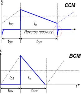
The first stage consists of full bridge diode rectifier and the power factor controlled boost converter see in fig. 2. The input 220 volts AC is converted into 220 volts DC by using full bridge diode rectifier. By converting AC-DC ripples will be produced in the rectifier output. AC-DC conversion is required because DC drive is used to operate the load. The Boost converter is a DC-DC converter. The ripples produced by the rectifier output can be decreased by PFC Boost converter which is operated in boundary conduction mode (BCM).
Fig. 2 Power factor controlled boost rectifier
Technology (IJRASET)
[image:4.612.198.458.175.475.2]convert AC voltage to DC voltage the voltage lag is occurred. To improve the power factor unity PFC correction is required in Boost converter. The power factor correction can be consider in the design of the driver, if they handled power is more than 60 watts. By operating the converter in BCM, high efficiency can be achieved by using ultrafast silicon diodes. The most commonly used operating modes of boost converter are boundary conduction mode and continuous conduction mode. These two names pass on to the current flowing through the inductor. The inductor current is continuous in CCM, while in BCM a new switching time is introduced when the current returns to zero which is at boundary of CCM and DCCM which is shown in fig 3.
Fig. 3 Wave forms for different modes of boost converter
III. ELECTRONIC TRANSFORMER
The second stage is an Electronic transformer, the main aim of second stage is to provide galvanic isolation and also determine the low frequency ripples which are presence in boost output. The output voltage of boost converter is given to electronic transformer. Due to the absence of electrolytic capacitor its output voltage will be expressed as
Vg=Vg-nom(1 + sin (2)) (3.1)
The relative value of the peak –peak ripple will be denoted as rv and the nominal output voltage will be denoted as Vg . Where
The ripples presence in the first stage output results will not affect the second stage results because of closed loop control will be fast enough to cancel this ripple. This topology plays a vital role in improving high efficiency and also it cancels the low frequency ripples.
Technology (IJRASET)
Here zero voltage switching concepts will be used to avoid overlapping. So, the gain of input and output is fixed. ZCS and ZVS concepts are used to reduce the losses. Due to the absence of filter inductor in outputs side resonance takes place, to avoid resonance ZCS should be used. ZCS can be calculated by using leakage inductance, dead time and frequency. So the load sharing between the two outputs must be carefully considered to achieve ZCS.
[image:5.612.221.425.154.341.2]400 volts input is given to ET. The capacitors which are used in the output side are 1 mF
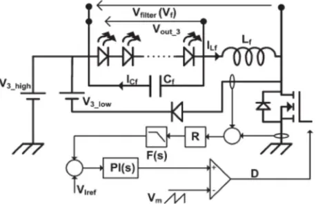
Fig. 4 Diagram of Electronic transformer
Fig. 5 Pulses of electronic transformer
IV. DRIVING TECHNIQUE
There are two driving techniques used in LEDs. They are Amplitude Mode and PWM mode driving technique. Amplitude mode driving is the preferred option because constant DC current is used to drive the LEDs. It provides high luminous intensity but it is weak in flexibility control. In PWM mode driving, pulse of DC current having zero level and high level are used. It provides flexible control and color stability but it provides low luminous intensity. In LED driving, luminous intensity is more important than others. So, we preferred Amplitude mode driving technique. LED luminous output depends on the further current flow through it. Due to The changes of input and the output voltages the precision value of output current can be easily affected. The current regulation can be achieved by continuously sensing the LEDs current by using resistor Rs and the voltage across the sense resistor is given to an
error amplifier.
To control the output current at different levels, an external voltage Vadj is used for varying the voltage across Rs. The relation
between Rs, Vadj and if are given in the following equation (4.1) & (4.2).
[image:5.612.137.507.380.504.2]Technology (IJRASET)
A=Rs/Rs+Radj (4.2)
The current level if changes inversely proportional to the Vadj, so luminous intensity also varied by varying LED current level. Due
to the presence of dynamic resistance of LEDs, a small voltage change in the converter will produce a large variation in the LED current.
V. TWO INPUT BUCK CONVERTER
[image:6.612.209.438.210.358.2]The third stage is responsible for eliminating the voltage ripple coming from the ET outputs by adjusting the each LED string current to the desired level. TIBuck converter s are some extant but similar to the conventional buck converters. Here the anode of the diode is connected to voltage V3-low lower than V3-high. TIBuck converter is shown in fig 6.
Fig. 6 Diagram of TI-Buck converter with driving technique for each LED string. Neglect the voltage drop across the diode and transistor then
Vout=DVin (5.1)
VI. PROPOSED TOPOLOGY AND SIMULATION RESULTS
The proposed three stage topology is developed by using MATLAB software. The input given to the PFC boost converter is 220 volts, 50 HZ AC supply. This 220volts AC supply is rectified by using single commutation (or full bridge rectifier) and then it will be boosted to 400volts by using boost converter. This boosted output voltage is given to electronic transformer nothing but 1:1 transformer. Electronic transformer has two outputs, the output voltages are 144 V and 80 V because LED strings need 130 V to fully turn on and 90 V to turn off. To achieve ZCS 200-nF capacitor is necessary in transformer. ET outputs are given as input to TIBuck converter. The four TIBuck converters are operated at 100 KHZ. The buck converter is made of 1 mF capacitor and inductance of 1.1 mH. A simple PI controller is implemented in each TIBuck converter because current can be independently controlled. Low voltage devices us to boost the efficiency.
[image:6.612.165.449.604.702.2]In these topology buck converter is designed 40 Watts per string. Here, 4 TIbuck converters are connected across the end terminals of the second stage. So, the total output is 160 Watts. The Fig 7 shows the proposed three stage topology MATLAB model.
Technology (IJRASET)
The boost converter is implemented with inductor value of 1.16 µH and capacitor value of 1 mF. The first stage has the efficiency of 97%, hence the single output size is not considerably increased but efficiency is increased.
The input voltage of diode rectifier, output voltage of diode rectifier, power factor correction and output voltage wave form of PFC boost convert as shown in fig 8,9,10,11.
Fig 8. Input voltage of diode rectifier
Fig 9. Output waveform of diode rectifier
Fig10. Power factor waveform
Fig11. Output voltage of boost converter
Technology (IJRASET)
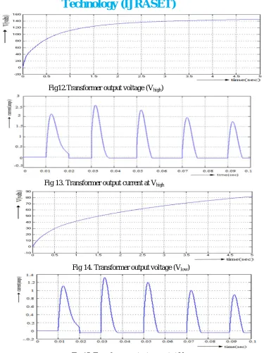
Fig12.Transformer output voltage (Vhigh)
Fig 13. Transformer output current at Vhigh
[image:8.612.138.513.62.563.2]
Fig 14. Transformer output voltage (Vlow)
Fig 15. Transformer output current at Vlow
[image:8.612.134.514.605.707.2]Technology (IJRASET)
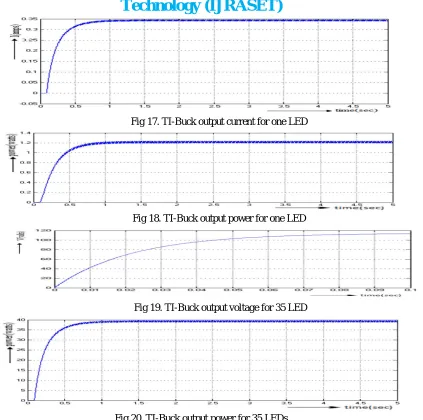
Fig 17. TI-Buck output current for one LED
Fig 18. TI-Buck output power for one LED
Fig 19. TI-Buck output voltage for 35 LED
Fig 20. TI-Buck output power for 35 LEDs
VII. CONCLUSION
LEDs are fast consideration in lighting by converting electrical energy into light. This new technology needs different power supplies from the rest of lighting devices. The main issues when analyzing these new converters are high efficiency, high reliability, and total dimming and color quality. In street lighting, quality of light is less importance than efficiency and reliability.
In this paper, LED based street lighting application is presented by using different converters without electrolytic capacitors. It is designed by using three stages. Each stage is designed for one specific task, in such a way that the overall efficiency is 93%. This topology is designed without electrolytic capacitor so reliability is high.
The simulation results have been obtained with a MATLAB designed for 4 X 40-W LED strings achieving efficiency at full load as high as 95% for the second and third stages in cascade. If the first stage is considered, the proposed three stage topology may reach efficiency as 93%.
VIII. ACKNOWLEDGEMENT
I would like to express special thanks to my advisor ‘Mr. G. KUMARA SWAMY’ Assoc. Prof in EEE dept, RGMCET, Nandyal, for continuous encouragement throughout the work.
REFERENCES
Technology (IJRASET)
[2] Huahuan LEI, Tao yu3, Lilan Liu “The Application of Multiple Attribute Decision in Led Commerce Platform” Telkomnika Vol. 11, No. 1, April 2013, pp. 2042 ~ 2049 e-ISSN: 2087-278X.
[3] Subramani Shanmugan, Devarajan Mutharasu “Performance of LED Employing Metal Oxide Mixed Thermal Interface Material by Structure Function Analysis” International Journal of Power Electronics and Drive System (IJPEDS) Vol.3, No.4, December 2013, pp. 409 – 417 ISSN: 2088-8694.
[4] Didier Balacco, and Almadidi Aguissa Diallo, “High efficiency LED driver without electrolytic capacitor for street lighting,” IEEE transactions on industry applications, VOL. 49, NO. 1, JANUARY/FEBRUARY 2013.
[5] T. Siew-Chong, “General n level driving approach for improving electrical-to-optical energy-conversion efficiency of fast-response saturable lighting devices,” IEEE Trans. Ind. Electron., vol. 57, no. 4,pp. 1342–1353, Apr. 2010.
[6] G. Linlin, R. Xinbo, X. Ming, and Y. Kai, “Means of eliminating electrolytic capacitor in AC/DC power supplies for LED lightings,” IEEE Trans. Power Electron., vol. 24, no. 5, pp. 1399–1408, May 2009.
[7] D. G. Lamar, J. Sebastián, A. Rodríguez, M. Rodríguez, and M. M.Hernando, “A very simple control strategy for power factor correctors driving high-brightness LEDs,” IEEE Trans. Power Electron., vol. 24,no. 8, pp. 2032–2042, Aug. 2009.
[8] H.Ma,W. Yu, C. Zheng, J.-S. Lai, Q. Feng, and B.-Y. Chen, “A universal input high-power-factor PFC pre-regulator without electrolytic capacitor for PWM dimming LED lighting application,” in Proc. IEEE ECCE,2011, pp. 2288–2295.
[9] Diego G. Lamar, Francisco F. Linera, Didier Balocco, Almadidi Aguissa Diallo, and Javier Sebasti “Design of a Soft-Switching Asymmetrical Half-Bridge Converter as Second Stage of an LED Driver for Street Lighting Application” IEEE Transactions On Power Electronics, Vol. 27, No. 3, March 2012
[10] W. Beibei, R. Xinbo, Y. Kai, and X. Ming, “A method of reducing the peak-to-average ratio of LED current for electrolytic capacitor-less AC-DC drivers,” IEEE Trans. Power Electron., vol. 25, no. 3, pp. 592–601, Mar. 2010.
[11] L.Xingming and Z. Jing, “An intelligent driver for light emitting diode street lighting,” in Proc. World Automation Congr. (WAC), 2008, pp. 1–5.
[12] W. Eberle, H. Yongtao, L. Yan-Fei, and Y. Sheng, “An overall study of the asymmetrical half-bridge with unbalanced transformer turns under current mode control,” in Proc. 19th Annu. IEEE Appl. Power Electron. Conf. Expo. (APEC), 2004, pp. 1083–1089.
[13] D. G. Lamar, J. Sebastian, M. Arias, and M. M. Hernando, “A low-cost AC-DC high-brightness LED driver with power factor correction based on standard peak-current mode integrated controllers,” in Proc. IEEE Energy Converts. Congr. Expo. (ECCE), 2010, pp. 463–470.
[14] J. Sebastian, P. J. Villegas, M. Hernando, F. Nuno, and F. Fernandez-Linera, “Average-current-mode control of two-input buck post regulators used in power-factor correctors,” IEEE Trans. Ind. Electron., vol. 46, no. 3, pp. 569–576, Jun. 1999.
[15] J. Sebastian, P. J. Villegas, F. Nuno, and M. M. Hernando, “High efficiency and wide-bandwidth performance obtainable from a two-input buck converter,” IEEE Trans. Power Electron., vol. 13, no. 4, pp. 706–717, Jul. 1998.
[16] Y. Wensong, L. Jih-Sheng, M. Hongbo, and Z. Cong, “High-efficiency DC-DC converter with twin bus for dimmable LED lighting,” IEEE Trans. Power Electron., vol. 26, no. 8, pp. 2095–2100, Aug. 2011.