Identification of Equivalent Circuit Based on Polygon Network
for Nonreciprocal Lossy
N
-Port Device
Leonardo Zappelli*
Abstract—In this paper, a technique to identify/synthesize an equivalent circuit of nonreciprocal lossy N-port device is presented. The technique joins the classical procedure discussed in the ’60s to the polygon network recently proposed in the literature, which permits to draw an equivalent circuit for reciprocal lossless N-port device in a very simple way. The identification is applied to two microwave devices, a reciprocal lossy iris in WR90 waveguide and a 3-port nonreciprocal lossy circulator. The proposed equivalent circuit could give some information about the agreement of the manufactured device and its design, which usually is developed in the hypothesis of ideal lossless components.
1. INTRODUCTION
In the past, many researchers have studied the equivalent circuits ofN-port microwave devices starting from the knowledge of the impedance matrix Z or scattering matrix S [1, 2]. Carlin proposed in ’50s–’60s an efficient approach to synthesize equivalent circuits based on 2N-ports transformer banks, which realize the desired circuit [3–6]. Cederbaum [7], Oono [8] and Youla et al. [9, 10] proposed some refinements to that approach to enhance the realization of the circuit. The main problem lies in the use of “complex transformers” [11] that cannot be realized in some scenarios. Moreover, the corresponding network can be very hard to manage if the device has many ports.
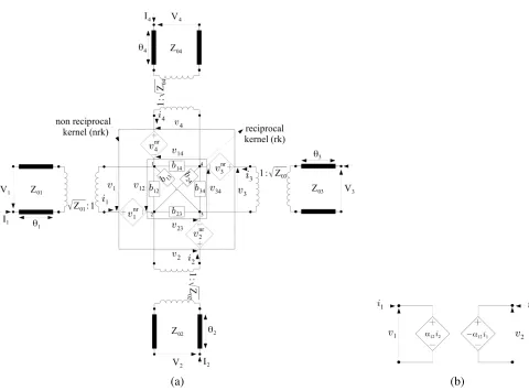
Recently, an equivalent circuit for lossless N-port S-matrix has been defined using a very simple and efficient synthesis technique [12], based on a polygon network, with susceptances placed at the sides and at the diagonals ofN-port polygon, and onN transmission lines connecting the device ports to the polygon sides. For example, the equivalent circuit for a 4-port device is shown in Fig. 1(a). A square is drawn, and six susceptances are placed at the sides and at the diagonals (the reciprocal kernel in Fig. 1(a)). Finally four transmission lines connect the external input ports of the device to the sides of the polygon. Transformers are used to normalize the susceptances contained in the kernel. The electrical parameters are ten as the ten scattering coefficients, because the S-matrix is symmetric, and they can be easily evaluated as described in [12]. This equivalent circuit is able to also include the presence of evanescent modes [13, 14], and it has been applied to some microwave discontinuities, as inductive/capacitive irises, bends and T-junctions [15]. Moreover, similar equivalent circuits have been defined to reconstruct the experimental S-matrix ofN-port device with measurements performed only with 2-port Vector Network Analyzer (VNA) [16].
For N-port reciprocal device, the equivalent circuit contains N input transmission lines and N(N −1)/2 susceptances, placed at the sides and at diagonals of N-side polygon. Globally, there areN(N + 1)/2 electrical parameters, corresponding exactly to theN(N+ 1)/2 scattering parameters of the reciprocalN-port device. The easiness of drawing the equivalent circuit of N-port device should be appreciated.
Received 3 April 2017, Accepted 12 June 2017, Scheduled 29 June 2017 * Corresponding author: Leonardo Zappelli ([email protected]).
(a) (b)
Figure 1. Equivalent circuits of (a) a reciprocal 4-port device and (b) a non reciprocal lossless gyrator.
The aim of this paper is to join these new equivalent circuits and the classical synthesis, replacing the transformer banks with the polygon network, that is easier to evaluate, to obtain a circuit able to represent the general case of nonreciprocal lossyN-port device. The equivalent circuit can be used in circuit synthesis or identification.
The circuit synthesis is the process that starts from the knowledge of a lossless S-matrix with the desired behavior and ends with the realization of a microwave device, usually assumed lossless in the design phase. In this case, the synthesized equivalent circuit gives the susceptance values that must be realized, for example, with irises, or cavities, or other microwave devices. The electrical lengths of the transmission lines in the circuit are the lengths of the waveguides that connect the N input ports to the circuit kernel, to obtain the desired phase relationships between ports. Nonreciprocity is obtained with gyrators connected to the circuit ports, realized with ferrite devices.
2. THEORY
2.1. Non Reciprocal Lossless Device
The first step to extend this equivalent circuit to any kind of device is to consider the case of a nonreciprocal lossless device. The simplest way is to remember that nonreciprocity can be added with a gyrator. A gyrator is a nonreciprocal lossless device that has the following normalized impedance
matrix
v1
v2
=ζgyr
i1 i2 =
0 α12 −α12 0
i1
i2
⇒
v1 =α12i2
v2 =−α12i1 (1)
Equation (1) represents two CCVSs (Current Controlled Voltage Source), at the two sides of the gyrator, which can be put in the form shown in Fig. 1(b). The amplitude α12 must be real to ensure that the
gyrator is lossless.
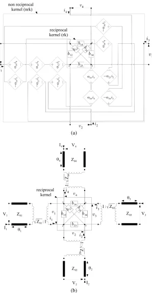
Hence, to introduce nonreciprocity in the equivalent circuit shown in Fig. 1(a), the current in each port must control a voltage source at the other ports. This implies the presence of N(N −1)/2 = 6 gyrators which must be placed at the ports of the circuit reciprocal kernel. Each gyrator relates the voltage at each nonreciprocal kernel port to the current in the other ports, as shown in Fig. 2(a). With the gyrators, the number of circuit parameters is N2 = 16, (4 transmission lines, 6 gyrators and 6 susceptances), just as the number of scattering parameters of a 4-port nonreciprocal device (equal to N2, withN = 4). In this sense, the proposed circuit is a minimal realization.
The kernel circuit in Fig. 2(a) appears complex, but it can be drawn in more readable form, if the voltage at each port of the gyrators is included in a global CCVS at the same port. In doing so, four CCVSs are placed at the input ports of the circuit kernel. CCVS placed at port 1 depends on the current of ports 2, 3 and 4, similarly, for the other CCVSs. Hence, the nonreciprocal equivalent circuit can be drawn as shown in Fig. 2(b), with:
vnr
1 = α12i2+α13i3+α14i4 (2)
vnr
2 = −α12i1+α23i3+α24i4 (3)
vnr
3 = −α13i1−α23i2+α34i4 (4)
vnr
4 = −α14i1−α24i2−α34i3 (5)
or
vnr
k =
N
j=k+1
αkjik− k−1
j=1
αjkik k= 1, . . . , N (6)
with N = 4 for Fig. 2(b). The nonreciprocal kernel (nrk) shown in Fig. 2(b) is the combination of the CCVS’s and the reciprocal kernel (rk), i.e., the polygon susceptance network. The normalized nonreciprocal Z-matrix of the nonreciprocal kernel, ζnrk, is obtained from the knowledge of ζrk, the reciprocal normalized Z-matrix of the reciprocal kernel, summing the effects of the gyrators:
⎡ ⎢ ⎣ v1 v2 v3 v4 ⎤ ⎥ ⎦=ζnrk
⎡ ⎢ ⎣ i1 i2 i3 i4 ⎤ ⎥ ⎦= ⎧ ⎪ ⎪ ⎪ ⎪ ⎪ ⎪ ⎨ ⎪ ⎪ ⎪ ⎪ ⎪ ⎪ ⎩ ζgyr ⎡ ⎢ ⎣
0 α12 α13 α14 −α12 0 α23 α24 −α13 −α23 0 α34 −α14 −α24 −α34 0
⎤ ⎥ ⎦+ ζrk j ⎡ ⎢ ⎣
x11 x12 x13 x14
x12 x22 x23 x24
x13 x23 x33 x34
x14 x24 x34 x44
⎤ ⎥ ⎦ ⎫ ⎪ ⎪ ⎪ ⎪ ⎪ ⎪ ⎬ ⎪ ⎪ ⎪ ⎪ ⎪ ⎪ ⎭ ⎡ ⎢ ⎣ i1 i2 i3 i4 ⎤ ⎥ ⎦ (7)
It should be noted that:
• the impedance matrixζnrk=ζgyr+ζrkis lossless, because the reciprocal partζrkis purely imaginary, andζgyr is lossless.
• ζnrk
ij =−(ζjinrk)∗, i.e.,ζnrkis a “skew-hermitian” matrix becauseζnrk=−(ζnrk)†(symbol†represents
(a)
(b)
Having defined the equivalent circuits, the identification/synthesis procedure must be defined, starting from the knowledge of the overall nonreciprocalS-matrix. As discussed in the Introduction, the synthesis procedure described in [3–11] is very effective, but it makes use of transformer banks which are not simple to synthesize if the device has many ports. Moreover, it does not respect the geometry of the device because that network is a combination of reactive elements, transformers and gyrators, which does not take into account the physical realization of the device. In fact, any microwave device is realized with input lines which connect the inner kernel to the external ports, in order to delete the effects of the modes below cutoff excited by the kernel of the device. The synthesis procedure described in [3–11] includes input lines in the overall device, which is represented with reactive elements and transformers and putting the nonreciprocal gyrators exactly at the input ports.
On the contrary, the equivalent circuit shown in Fig. 2(b) takes into account the presence of the input lines and represents only the nonreciprocal kernel with gyrators and a polygon network as should be, for example, for a waveguide gyrators, where the nonreciprocity is due to the ferrite placed in the kernel of the actual device.
The synthesis procedure starts from the evaluation of the sum of the voltage drops at the ports of the nonreciprocal kernel. In fact, from the definition of ζnrk, Equation (7),
v1+v2+v3+v4 = 4
i=1
ζnrk i1 i1+
4
i=1
ζnrk i2 i2+
4
i=1
ζnrk i3 i3+
4
i=1
ζnrk
i4 i4 (8)
and from the analysis of the circuit shown in Fig. 2(b) and from Equations (2)–(5) v1+v2+v3+v4 = v12+v1nr+v23+v2nr+v34+vnr3 +v41+v4nr
= (v12+v23+v34+v41) +v1nr+vnr2 +vnr3 +v4nr= 0 +v1nr+vnr2 +v3nr+v4nr
=
4
i=1
αi1i1+ 4
i=1
αi2i2+ 4
i=1
αi3i3+ 4
i=1
αi4i4 (9)
withαii= 0 andαji=−αij, ifj > i. Equations (8) and (9) give
4
i=1
ζnrk i1 i1+
4
i=1
ζnrk i2 i2+
4
i=1
ζnrk i3 i3+
4
i=1
ζnrk i4 i4=
4
i=1
αi1i1+ 4
i=1
αi2i2+ 4
i=1
αi3i3+ 4
i=1
αi4i4 (10)
If we suppose to excite the device at one port at time, we obtain four conditions on each column ofζnrk:
v1+v2+v3+v4
i1 = 4 i=1 ζnrk i1 =
4
i=1
αi1 ∈ if i2 =i3 =i4 = 0 ∀i1 ⇒Im
4 i=1 ζnrk i1
= 0 (11)
v1+v2+v3+v4
i2 = 4 i=1 ζnrk i2 =
4
i=1
αi2 ∈ if i1 =i3 =i4 = 0 ∀i2 ⇒Im
4 i=1 ζnrk i2
= 0 (12)
v1+v2+v3+v4
i3 = 4 i=1 ζnrk i3 =
4
i=1
αi3 ∈ if i1 =i2 =i4 = 0 ∀i3 ⇒Im
4 i=1 ζnrk i3
= 0 (13)
v1+v2+v3+v4
i4 = 4 i=1 ζnrk i4 =
4
i=1
αi4 ∈ if i1 =i2 =i3 = 0 ∀i4 ⇒Im
4 i=1 ζnrk i4
= 0 (14)
Equations (11)–(14) are the key to evaluate the electrical lengths θ1, θ2, θ3, θ4, starting from the
knowledge of theS-matrix of the overall non reciprocal lossless device, namedSnr. In fact, the electrical
lengthsθ1, θ2, θ3, θ4 must have values such that the imaginary part of the normalized impedance matrix
ζnrk must satisfy Equations (11)–(14).
Hence, if we connect numerically four lines with negative electrical lengths −θ1,−θ2,−θ3,−θ4 to
the input ports of Snr, we obtain a new S-matrix which coincides with S-matrix of the nonreciprocal kernel, Snrk, if and only if the associated Z-matrix, ζnrk, satisfies Equations (11)–(14)
Im N i=1 ζnrk ij
being
ζnrk = I−Snrk−1Snrk+I (16)
Snrk = diagejθ1, ejθ2, ejθ3, ejθ4·Snr·diagejθ1, ejθ2, ejθ3, ejθ4 (17)
I is the 4×4 Identity Matrix, and diag is a 4×4 Diagonal Matrix with entries contained in the brackets. Equations (15) represent a system of four equations in four unknowns,θ1, θ2, θ3, θ4, which can be solved
numerically. Equations (15)–(17) replace the condition on theS-matrix (orZ-matrix) discussed in [12] for the reciprocal case.
Once the values ofθ1, θ2, θ3, θ4 have been obtained,ζnrk can be extracted by Equations (16)–(17).
From Equation (7), CCVS’s values and the reciprocalZ-matrix of the polygon network in Fig. 2(b) are
⎡ ⎢ ⎣
0 α12 α13 α14 −α12 0 α23 α24 −α13 −α23 0 α34 −α14 −α24 −α34 0
⎤ ⎥
⎦ = Re
ζnrk (18)
ζrk = jImζnrk (19)
The susceptances contained in the polygon network can be evaluated solving a linear equation system, starting from the knowledge ofζrk, Equation (19), as described in [12]. The circuit parameters evaluated in the identification/synthesis procedure are related to the “kind” of the analyzed device. Hence, they can be constants or varied with the frequency, depending on the actual device.
Obviously, Equations (15)–(17) can be easily extended to the case of N-port device, replacing 4 withN. In this case, the equivalent circuit containsN2 electrical parameters, just as the number of the scattering parameters of theN ×N S-matrix. In fact, the total number of the circuit parameters are:
• N transmission lines of electrical lengthsθk, k= 1,2, . . . , N, connecting the input ports to the non reciprocal kernel.
• NN−1
2 gyrators placed at the ports. In fact, in the hypothesis that a gyrator links portito portj: – N −1 gyrators are placed at the first port (to link the first port to the other N−1 ports).
– N−2 gyrators are placed at the second port (to link the second port to the otherN−2 ports, except the first port that is linked with the gyrator described in the previous item).
– N −3 gyrators are placed at the third port (to link the third port to the other N −3 ports, except the first and the second ports that are linked with the gyrators described in the two previous items).
– . . ..
– 1 gyrator is placed at portN −1 (to link the portN −1 to the last port).
• N susceptances placed at the side of the polygon and NN−23 susceptances placed at the polygon diagonals (overallNN−21 susceptances).
The sum of the electrical parameters is: N (electrical lengths) +NN2−1 (gyrators) +N (susceptances at sides) +NN2−3 (susceptances at diagonals) =N2. Hence, the proposed equivalent circuit is a minimal representation for any N-port non reciprocal lossless device.
2.2. Nonreciprocal Lossy Device
The power loss in actual microwave device is due to the presence of waveguide discontinuities (inductive/capacitive irises, cavities, . . .) in the device kernel where the field can be very strong. For example, in a capacitive diaphragm the electric field is perpendicular to the edges of the metallic partitions of the waveguide. On these edges, the electric field (sum of the incident and reflected fundamental mode and the excited evanescent modes) tends to be very strong, and it causes a “large” amount of power loss just on the diaphragm surface.
the classical approaches described in [1, 2]. This effect becomes substantial if the electromagnetic field propagates up and down many times, as it happens in a cavity, but it can be neglected if the electromagnetic field travels only one or two times in the waveguide, as in the input lines of the device. In fact, in these lines the electromagnetic field associated with the fundamental mode travels towards the kernel of the device is reflected and travels backwards the input port. Hence, for only two travels, the losses due to the conducting waveguide walls can be neglected, and the input lines can be considered lossless. Hence, the equivalent circuit should satisfy such a characteristic, and it should include the loss only in the kernel.
Starting from the circuit developed in Subsection 2.1, we can expect that the Z-matrix of the kernel device will be a complex quantity. A first hypothesis to define the lossy equivalent circuit can be to replace the susceptances of the polygon network with admittances, where the conductances should represent the effect of the power loss. This approach can be easily developed, but it causes a non-realizable equivalent circuit, because some conductances are positive while others are negative. The global amount of loss is exactly that imposed by the actual device, but this circuit implies the presence of active device that is not present in actual device. Hence, this simple approach is not correct.
The solution lies in following the approach developed in [3, 10] which suggests to represent the Z-matrix of the nonreciprocal lossy kernel,ζlnrk, which relates voltages vi and currentsii,i= 1,2, . . . , N,
at the ports of the nonreciprocal lossy kernel, as the series of two Z-matrices:
ζlnrk = ζnrk+ζloss (20)
ζnrk = 1
2
ζlnrk−ζlnrk†
(21)
ζloss = 1
2
ζlnrk+ζlnrk†
(22)
The first, ζnrk, is the Z-matrix of the nonreciprocal lossless kernel relating voltages vnrki and currents ii, and the second,ζloss, is theZ-matrix of the nonreciprocal lossy kernel of the device relating voltages
vloss
i and currentsii. Some properties ofζnrk and ζloss should be highlighted: • from Equation (21),ζnrkis a lossless “skew-hermitian” matrix and satisfies
ζnrk=−ζnrk† (23)
with Re[ζiinrk] = 0, i.e., the elements of the main diagonal are imaginary numbers. Moreover, ζnrk
ji =−
ζnrk ij
∗
, or ζjinrk=−αij +jxij andζijnrk=αij +jxij.
• from Equation (22),ζloss is a lossy “hermitian” matrix and satisfies
ζloss=ζloss† (24)
withζjiloss= (ζijloss)∗ and Im[ζlossii] = 0, i.e., the elements of the main diagonal are real numbers.
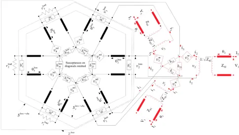
Hence,ζnrk is the lossless skew-hermitian Z-matrix which has been discussed in Section 2.1, and it can be identified with the equivalent circuit of Fig. 2(a), with the input lines being lossless, as previously discussed. Joining this circuit and Equation (20), the 4-port equivalent circuit proposed in this approach to solve the case of nonreciprocal lossy device is shown Fig. 3, where ζnrk and ζloss represent the Z -matrices to be realized.
The four lines with electrical lengths θ1, θ2, θ3, θ4 are obtained applying conditions in Eqs. (15)–
(17) toζnrk, andζnrk is represented with gyrators and the susceptances polygon network, as previously discussed. The secondZ-matrix,ζloss, can be realized with an equivalent circuit with susceptances and
resistance because it is a matrix of positive definite or semi-definite hermitian form [3, 8].
Figure 3. The equivalent circuit of 4-port non reciprocal lossy device.
• evaluation of theS-matrix Sloss→dia which transformsζloss in a diagonal matrix, Equation (A11)
Sloss→dia=
04×4 u
u† 0 4×4
(25)
whereu is the 4×4 matrix containing the eigenvectors ofζloss, written as columns.
• mathematically connect 2N = 8 admittances −jbzi, i= 1,2, . . . ,2N to the 2N ports of Sloss→dia, obtaining a new S-matrix Sloss→dia
z which can be realized with a 2N-port susceptances polygon
network and 2N transmission lines. The choice of bz
• once the polygon network has been evaluated, connect 2N admittances jbzi,i = 1, . . . ,2N to the corresponding 2N ports
• load the outputN = 4 ports with N resistive loadsrloadi , equal to the i-th eigenvalue ofζloss, for i= 1, . . . , N.
The resulting equivalent circuit of ζloss is shown in Fig. 4, where CCVSs are related to the gyrator amplitudes αlosskj , evaluated in the identification of ζloss, as discussed in Subsection 2.1:
vnrl
k =−
k−1
j=1
αloss jk ik+
2N
j=k+1
αloss
kj ik k= 1,2, . . . ,2N (N = 4) (26)
This procedure ends the identification process.
(a) (b)
Figure 5. (a) Square reciprocal iris (side 19 mm, depth 15 mm) inserted between two rectangular WR90 waveguides. (b) 3-port circulator in rectangular WR90 waveguide.
Ls
Cs
Cp Lp
(a) (b)
Figure 6. (a) The equivalent circuit of 2-port reciprocal lossy iris in WR90 waveguide. The lossless skew-hermitian part is drawn with red color and the lossy hermitian part with black color. (b) Realization of the susceptancebp contained in the skew-hermitian lossless part of the equivalent circuit.
3. RESULTS
and the corresponding electrical parameters are shown in Fig. 7. The normalized susceptancesbzi which delete the eigenvalueλ= 1 of order 2 inSloss→diahave been chosen to ensure that the diagonal elements of Szloss→dia have equal magnitude: bzi = 0.535, i = 1,2,3,4. In doing so, some symmetries in the equivalent circuit of the lossy part can be obtained. In fact, it can be seen from Figs. 7(a)–7(b) that θloss
1 =θ3loss, θ2loss=θloss4 andbloss12 =bloss14 , bloss23 =bloss34 . Obviously, other choices for bzi are permitted.
The resistive loads shown in Fig. 7(c) are not equal because of the presence of measurement errors at the two ports of VNA and a non-perfect connection between the iris and the two waveguides.
In fact, a small misalignment causes a different effect on the losses at the two front surfaces of the iris, producing a small difference between the measuredS11exp lossyandS22exp lossy, as shown in Fig. 7(d) (black and blue dotted lines). This misalignment is confirmed also by the little spike appearing in
Sexp lossy 11 ,S
exp lossy 12 ,S
exp lossy
22 at about 11.2 GHz. In fact, modes TE11 and TM11 of the square iris
(a) (b)
(c) (d)
have a frequency cutoff at about 11.16 GHz. If the alignment were perfect, these modes should not be excited by the discontinuity. Hence, the little spike at about 11.20 GHz means that these modes are excited by a little misalignment between the iris and the two waveguides. The effect of this spike is evident in the electric circuit parameters shown in Figs. 7(a)–7(d). Finally, the misalignment accounts for the little difference between θ1 and θ2 in Fig. 7(a), which should be equal for a centered iris.
The normalized susceptances bp relative to the lossless skew-hermitian part can be realized with the circuit shown in Fig. 6(b), with Ls = 5.63 ·10−12, Cs = 9.95 ·10−9, Lp = 1.49 ·10−12, and Cp= 1.05·10−10. The normalized susceptancesblossij and load resistances relative to the lossy hermitian part have a behavior quite difficult to be realized with the same precision used forbp. Anyway, the effect of the lossy part is small compared to the lossless part of the circuit, because the iris has a low amount of loss. Hence, these electrical parameters can be approximated with a constant value obtained with an integral mean over the whole band: r1 ≈0.029, r2 ≈0.012, bloss12 =bloss14 ≈1.42, b23loss =bloss34 ≈3.63,
bloss
13 ≈ −2.52,bloss24 ≈ −3.54. The S-matrix obtained with these inductances/capacitances/resistances is
in a very good agreement with the experimental results shown in Fig. 7(d) (about±0.15 dB), and they are not shown for simplicity.
During measurements, the effect of the losses cannot be deleted, because they are inseparable from the actual device, but it is interesting to wonder what happens if the lossy part of the equivalent circuit is deleted, replacing rload1 and r2load with short circuits. The readers may think that the “experimental results for lossless” iris are obtained. Hence, the scattering coefficients for the “experimental lossless” iris, obtained with that replacement, have been evaluated, and they are shown in Fig. 7(d) with continuous lines. The “experimental lossless” and the CST simulations (dashed lines) for the lossless iris are very close in Fig. 7(d). Hence, from the experimental results on lossy device, the “experimental lossless” results can be evaluated from the equivalent circuit and compared with numerical simulations in order to understand how close the simulations are to the “experimental lossless” device, which can never be measured because the losses are unavoidable. If they are very close, the differences between the
(a) (b)
(c) (d)
(g) (h)
(i)
Figure 9. (a)–(f) Electrical lengths, gyrators and susceptances of the equivalent circuit shown in Fig. 8, relative to the circulator of Fig. 5(b). (g) Resistive loads of the equivalent circuit shown in Fig. 8, relative to the circulator of Fig. 5(b). (h) The experimental scattering coefficients of the circulator. (i) The scattering coefficients of the “experimental lossless” circulator, obtained from the circuit of Fig. 8 replacing the resistive loads with short circuits, to delete the effect of the losses.
experimental lossy results and the numerical simulations are simply due to the device loss. Otherwise, there can be some discrepancy between the realized irises and those obtained in the phase design. This can enhance the optimization of filters, diplexers and other devices.
The second analyzed device is the 3-port circulator in WR90 rectangular waveguide acting in the X-band, shown in Fig. 5(b). The experimental results for the 3-port circulator shown in Fig. 9(h) have been used to identify the circuit shown in Fig. 8: the nonreciprocal lossless skew-hermitian part is identified with a triangle of susceptances and three CCVSs at its ports (right side of the figure, red color); the nonreciprocal lossy hermitian part is identified with a polygon network with six sides and three ports (4,5,6) closed on three resistive loads, equal to the eigenvalues of ζloss (left side of the figure, black color). The normalized susceptances bzi which delete the eigenvalue λ= 1 of order 3 in Sloss→dia have been chosen equal to bz
susceptances, gyrator amplitudes and resistive loads are shown in Figs. 9(a)–9(g). It is interesting to evaluate the “experimental lossless” case, obtained replacing the three resistive loads with short circuits: these results are shown in Fig. 9(i). It should be noted that the “experimental lossless” circulator works well in the band 9.3–9.5 GHz, where|S12|,|S23|,|S31|are very similar, as declared by the manufacturer (see Fig. 5(b)). Hence, design is probably correct. On the other hand, comparing 9(h) and 9(i), it is evident that the losses act on|S12|in a different way from that on|S23|and|S31|. This behavior can be of interest for the manufacturer, which can enhance the circulator design to make|S12| ≈ |S23| ≈ |S31| in the band of interest.
4. CONCLUSIONS
The equivalent circuit for nonreciprocal lossy N-port device has been obtained joining the classic synthesis technique and the recent polygon network, which permits to draw the equivalent circuit in a very simple way for any number of ports. The technique has been applied to the identification of the equivalent circuit of a reciprocal lossy iris and of a non reciprocal lossy 3-port circulator. The equivalent circuit can permit to delete the effect of the losses replacing the resistive loads, which represent the loss, with short circuits, to enhance the design of the device, which is usually done in the hypothesis of lossless components.
APPENDIX A.
The procedure to synthesize ζloss is little bit complex, and some preliminary remarks must be done. Hermitian nonreciprocal Z-matrix ζloss, Equation (22), relates the voltages at the input, vlossi , i= 1,2,3,4, to the currentii, as shown in Fig. 3:
vloss =
⎡ ⎢ ⎢ ⎢ ⎢ ⎣
vloss 1
vloss 2
vloss 3
vloss 4
⎤ ⎥ ⎥ ⎥ ⎥
⎦=ζ
lossi=ζloss
⎡ ⎢ ⎣
i1
i2
i3
i4
⎤ ⎥
⎦ (A1)
The identification of ζloss is not simple as ζnrk, becauseζlosssatisfies Equation (24), which implies that the nonreciprocity afflicts the imaginary part of ζloss. Hence, non reciprocity of ζloss cannot be represented with real gyrators as done for ζnrk.
However, a solution can be found if a transformation on voltages viloss and currents ii is applied,
as suggested in [3, 8]. To do this, we must observe that ζloss is a Positive Definite (PD) matrix of an hermitian form, because it is related to the dissipated power in the device. In fact, ifζloss is excited by N currents, say the vector iexc of dimensionsN ×1, the dissipated power in ζloss,Ploss, is
Ploss = (iexc)†ζlossiexc (A2)
which is always a positive real quantity. This is just the definition of a Positive Definite hermitian matrix that has some properties [17]:
• the eigenvalues of a matrix of an hermitian PD form (ζloss) are always positive;
• if the eigenvectors ofζloss are written as the columns of a matrixu, then
u u†=u† u=I ⇒u−1 =u† (A3)
• a matrix of an hermitian PD form (ζloss) can be diagonalized with the help of its eigenvectors. In
fact, if the eigenvectors are put in the columns of the matrixu, it is possible to define a diagonal matrix from ζloss such that
ζloss =u ζdiau† ⇒ ζdia=u†ζloss u (A4)
From Equations (A1) and (A4):
vloss=ζloss i=u ζdia u† i (A5)
or
u−1 vloss=u† vloss=ζdia u† i (A6)
Setting
vdia = u†vloss (A7)
idia = u†i (A8)
we obtain,
vdia =ζdia idia= diagλζloss 1 , λζ
loss 2 , λζ
loss 3 , λζ
loss 4
idia= diagrload
1 , rload2 , rload3 , rload4
idia (A9)
where λζiloss is the i-th eigenvalue of ζloss. Equations (A7)–(A8) represent a linear transformation between (vloss, i) and (vdia, idia), which are related by Equation (A9), representing a diagonal matrix, ζdia, that connects the voltage at thei-th port to the current at the same port with a resistor equal to
thei-th eigenvalue ofζloss, as shown in Fig. A1(a).
(a) (b)
Figure A1. (a) Transformation of the hermitian matrix ζloss into the diagonal matrix ζdia connected to resistive loads. (b) Insertion of shunt susceptances at the ports of Sloss→dia to define theS-matrix Sloss→dia
z which can be realized with a polygon susceptances network.
The linear transformation in Equations (A7)–(A8) can be represented by the following matrix
vdia
idia
=
u†N×N 0N×N 0N×N u†N×N
vloss
i
=Tloss→dia
vloss
i
(A10)
First of all, the lossless S-matrix corresponding to Tloss→dia is:
Sloss→dia=
04×4
u†−1
u† 04×4
=
04×4 u
u† 0 4×4
(A11)
whereu is the 4×4 matrix containing the eigenvectors of ζloss, written as columns.
In order to obtain the lossless matrix Sloss→dia, the eigenvectors of ζloss must be normalized to ensure that the sum of the squares of the magnitude components of each eigenvector is equal to 1:
4
k=1|uki|2 = 1, i= 1,2,3,4. In fact Sloss→dia·Sloss→dia† =
04×4 u
u† 04×4 0u4׆4 04u×4
†
=
04×4 u
u† 04×4 0u4׆4 04u×4
= diag
4
k=1
|uk1|2, 4
k=1
|uk2|2, 4
k=1
|uk3|2, 4
k=1
|uk4|2,
4
k=1 |uk1|2,
4
k=1 |uk2|2,
4
k=1 |uk3|2,
4
k=1 |uk4|2
=I (A12)
Recalling that for a block matrix
det [M] = det [M22] det
!
M11−M12M22−1M21
"
(A13)
where Mij are the blocks of matrixM, the eigenvalues of Sloss→dia are obtained from Equations (A3) and (A11):
det
Sloss→dia−λI = det
−λI4×4 u
u† −λI4×4
= det [−λI4×4] det
−λI4×4−u(−λI4×4)−1u†
= λ4det
−λI4×4+u
#
I4×4
λ
$
u†=λ4det
1−λ2I4×4
λ
=
= 1−λ24 = 0 (A14)
Hence the eigenvalues of Sloss→dia are λ = ±1 with order 4 and, by this reason, it is not possible to obtain the correspondingZ-matrix,ζloss→dia, from Sloss→dia. In fact, the following relation holds
ζloss→dia=I−Sloss→dia−1Sloss→dia+I (A15)
and it is necessary thatI−Sloss→diais nonsingular, i.e., det(I−Sloss→dia)= 0. IfSloss→diahas eigenvalue λ= 1, from Equation (A14) it follows that det(I−Sloss→dia) = 0 and ζloss→dia can not be defined. In this case, it is not possible to define the polygon network susceptances directly fromSloss→dia, because such polygon network requires the definition of a Z-matrix.
Anyway, we can put at each port of Sloss→dia a shunt of two admittances, jbzi and −jbzi, without changing Sloss→dia, as shown in Fig. A1(b). If we include the eight admittances −jbzi in Sloss→dia we obtain a new S-matrix,Slossz →dia, with all eigenvalues other than 1, as discussed in Appendix B. This ensures that the Z-matrix ζzloss→dia exists and that Szloss→dia can be identified with the susceptances polygon network and transmission lines. Actually only four admittances −jbzi are sufficient to obtain the S-matrix Szloss→dia with all eigenvalues other than 1, but we prefer to include 8 admittances to impose some symmetry properties toSzloss→dia (for example, that all the diagonal elements ofSzloss→dia have the same magnitude).
Hence, to realize ζloss the following procedure applies (N = 4 in Fig. A1):
• evaluation of the scattering matrix Sloss→dia which transforms ζloss in a diagonal matrix, based on the eigenvectors ofζloss, as shown in Equation (A11).
• mathematically connect 2N admittances −jbzi, i = 1,2, . . . ,2N to the 2N ports of Sloss→dia, obtaining the newS-matrix Sloss→dia
z which can be realized with a 2N-port susceptances polygon
network and 2N transmission lines. The choice of bz
• once the polygon network has been evaluated, connect 2N admittances jbzi,i = 1, . . . ,2N to the corresponding 2N ports.
• load the output N ports with N resistive loads riload, equal to the i-th eigenvalue of ζloss, for i= 1, . . . , N.
The resulting equivalent circuit ofζloss is shown in Fig. 4, where the CCVS’s are related to the gyrator
amplitudes αlosskj , evaluated in the identification of ζloss, as discussed in Subsection 2.1:
vnrl
k =−
k−1
j=1
αloss jk ik+
2N
j=k+1
αloss
kj ik k= 1,2, . . . ,2N (N = 4) (A16)
APPENDIX B.
In this appendix, it is shown that the 2N-port S-matrix Sloss→dia, which does not posses the correspondingZ-matrix becauseSloss→dia−I is singular, can be transformed in a new matrix Szloss→dia, withSzloss→dia−I not singular, connectingN admittances jbk,k= 1,2, . . . , N to N ports of Sloss→dia. The 2N-port S-matrix Sloss→dia has N eigenvalues equal to 1 and N eigenvalues equal to −1, as discussed in Appendix A, Equation (A14). The matrix can be divided in blocks as follows
Sloss→dia =
0N×N uN×N u†N×N 0N×N
=
⎡ ⎢ ⎣
0N×N uN×N−1 uLCN×1
u†N−1×N 0N−1×N−1 0N−1×1
u†,LR
1×N 01×N−1 01×1
⎤ ⎥ ⎦= = S11
(2N−1)×(2N−1) S 12 (2N−1)×1
S21
1×(2N−1) 01×1
(B1)
where u†N−1×N and uN×N−1 are blocks u†N×N and uN×N without the last row, u†1,×LRN, and the last
column, uLCN×1, respectively. Matrixu satisfies the following conditions:
1) I =u u†=! uN×N−1 uLCN×1
" u†N−1×N u†,LR
1×N
=
uN×N−1u†N−1×N+uLCN×1u†, LR 1×N
(B2)
2) rank
uN×N−1u†N−1×N
=N −1⇒det
uN×N−1u†N−1×N
= 0 (B3)
3) rank
uLC N×1u†,
LR 1×N
= 1⇒det
uLC N×1u†,
LR 1×N
= 0 (B4)
Condition 2) is obtained recalling that for a matrix A, rank[AA†] = rank[A], [18], and condition 3) holds because all columns ofuLCN×1u†1,×LRN are equal to column vectoruLCN×1 timesuk1, beingkthe column
index, and its rank is equal to 1.
If the last port of Sloss→dia is connected to a shunt admittance jb(Fig. A1(b)), with S-matrix Sb equal to
Sb =
S11 b Sb12
S12 b Sb11
= ⎡ ⎢ ⎢ ⎣ − jb
2 +jb 2 2 +jb 2
2 +jb − jb 2 +jb
⎤ ⎥ ⎥ ⎦ (B5) with S11
b Sb11−Sb12Sb12 = −Sb11−Sb12 (B6)
S12
b −Sb11 = 1 (B7)
the new overall S-matrix,Szloss→dia, is:
Sloss→dia z =
S11+S11
b S12S21 Sb12S12
S12
b S21 Sb11
The eigenvalues of Szloss→dia are obtained from (A13):
det
Sloss→dia z −λI
= det!Sb11−λ"det
S11+S11
b S12S21−λI2N−1×2N−1−S12Sb12
1 S11
b −λS 21S12
b
= det
!
S11
b −λ S11+Sb11S12S21−λI2N−1×2N−1
−S12S12 b S21Sb12
"
S11 b −λ
2N−2
= det
!
S11
b −λ S11−λI2N−1×2N−1
+S12S21Sb11Sb11−Sb11λ−Sb12Sb12"
S11 b −λ
2N−2 (B9)
From Equation (B1), S12S21is the following (2N−1) square matrix
S12S21=
uLC N×1u†,
LR
1×N 0N×N−1
0N−1×N 0N−1×N−1
(B10)
and, from Equations (B1), (B6) and (B7), the matrix A = (Sb11 − λ)(S11 − λI2N−1×2N−1) +
S12S21(S11
b Sb11−Sb11λ−Sb12Sb12) in Equation (B9) can be written as:
A=
uLC N×1u†,
LR 1×N
−S11
b −Sb12−Sb11λ
−S11 b −λ
λIN×N Sb11−λuN×N−1
S11 b −λ
u†N−1×N −
S11 b −λ
λIN−1×N−1
(B11)
Hence, from Equation (A13), (B2), (B6), (B7),
det
Sloss→dia−λI = det
!
−S11 b −λ
λIN−1×N−1
"
S11 b −λ
2N−2 det
uLC N×1u†,
LR 1×N
−S11
b −Sb12−S11b λ
−S11
b −λλIN×N+Sb11−λ2uN×N−1IN−1×N−1
S11 b −λ
λu†N−1×N
=
S11 b −λ
N−1
(−λ)N−1
S11 b −λ
2N−2 det
S11
b +Sb12+Sb11λ uN×N−1u†N−1×N −IN×N
−S11
b −λλIN×N+uN×N−1u†N−1×N
S11 b −λ
λ = det
IN×Nλλ2−2Sb11λ−Sb11−Sb12
+uN×N−1u†N−1×NSb11
λ2+ 2λ+ 1
λλ−S11 b
N−1
= det
IN×Nλ(λ+ 1)λ−1−2Sb11
+uN×N−1u†N−1×NSb11(λ+ 1)2
λλ−S11 b
N−1
=
(λ+ 1)Ndet
IN×Nλλ−1−2Sb11+uN×N−1u†N−1×NSb11(λ+ 1)
λλ−S11 b
N−1 (B12)
Equation (B12) has:
• N roots λ=−1, due to factor (λ+ 1)N, as the matrix Sloss→dia;
• N−1 roots λ= 1. In fact, forλ= 1 and from Equations (B2) and (B3), Equation (B12) becomes
det
2S11 b
−IN×N +uN×N−1u†N−1×N
= det
−2S11
b uLCN×1u†, LR 1×N
= 0 (B13)
• one root λ= 1 + 2S11b . In fact, forλ= 1 + 2Sb11 and from (B4), Equation (B12) becomes
det
uN×N−1u†N−1×NSb11
1 +Sb11= 0 (B14)
and λ= 1 + 2Sb11 is a simple root because the N ×N matrix uN×N−1u†N−1×N has rank equal to
N−1.
Hence, the shunt admittancejbconnected to port 2N has changed the order of the rootλ= 1 toN−1. If otherN −1 shunt susceptances are connected to other ports, we can delete all the roots λ= 1 from Sloss→dia
z −I, obtaining det[Slossz →dia−I]= 0. In doing so,Szloss→dia possesses aZ-matrix and it can be
represented with the polygon susceptance network.
REFERENCES
1. Marcuvitz, N., Waveguide Handbook, Mc-Graw-Hill, New York, 1951.
2. Montgomery, C. G., R. H. Dicke, and E. M. Purcell,Principles of Microwave Circuits, 1st Edition, McGraw-Hill, 1948; Peter Peregrinus on Behalf of the Institution of Electrical Engineers, 2nd Edition, London, U.K., 1987.
3. Carlin, H., “On the physical realizability of linear non-reciprocal networks,” Proceedings of the IRE, Vol. 43, No. 5, 608–616, May 1955.
4. Carlin, H., “The scattering matrix in network theory,”IRE Transactions on Circuit Theory, Vol. 3, No. 2, 88–97, Jun. 1956.
5. Carlin, H. and D. Youla, “Network synthesis with negative resistors,” Proceedings of the IRE, Vol. 49, No. 5, 907–920, May 1961.
6. Carlin, H., “On the existence of a scattering representation for passive networks,” IEEE Transactions on Circuit Theory, Vol. 14, No. 4, 418–419, Dec. 1967.
7. Cederbaum, I., “On the physical realizability of linear nonreciprocal networks,” IRE Transactions on Circuit Theory, Vol. 3, No. 2, 155–155, Jun. 1956.
8. Oono, Y., “Application of scattering matrices to the synthesis of n ports,” IRE Transactions on Circuit Theory, Vol. 3, No. 2, 111–120, Jun. 1956.
9. Youla, D., L. Castriota, and H. Carlin, “Bounded real scattering matrices and the foundations of linear passive network theory,” IRE Transactions on Circuit Theory, Vol. 6, No. 1, 102–124, Mar. 1959.
10. Youla, D., “Direct single frequency synthesis from a prescribed scattering matrix,” IRE Transactions on Circuit Theory, Vol. 6, No. 4, 340–344, Dec. 1959.
11. Carlin, H. and D. Youla, “The realizability of the complex ideal transformer,” IRE Transactions on Circuit Theory, Vol. 9, No. 4, 412–412, Dec. 1962.
12. Zappelli, L., “Simple, fast, and effective identification of an equivalent circuit of a waveguide junction withN ports,”IEEE Transactions on Microwave Theory and Techniques, Vol. 63, No. 1, 48–55, Jan. 2015.
13. Zappelli, L., “An equivalent circuit for discontinuities exciting evanescent accessible modes,”IEEE Transactions on Microwave Theory and Techniques, Vol. 60, No. 5, 1197 –1209, May 2012.
14. Zappelli, L., “Circuit approach to the analysis of microwave discontinuities,” Progress In Electromagnetics Research B, Vol. 53, 373–397, 2013.
15. Zappelli, L., “An equivalent circuit for thick centered irises in rectangular waveguide,” Proceedings of Numerical Electromagnetic Modelling and Optimization (NEMO), Pavia, 2014.
16. Zappelli, L., “Reconstruction of the S-matrix of N-port waveguide reciprocal devices from 2-port VNA measurements,”Progress In Electromagnetics Research B, Vol. 72, 129–148, 2017.
17. Gantmacher, F.,The Theory of Matrices, Chelsea Publishing Company, New York, 1959.