Design Analysis and Implementation of low
Component Count High Performance Offline
Power Supply for Digital Controller
Ashna Sidhiq1, Chandrasekar V2
PG Student [Power Electronics], Dept. of EEE, SJCET Palai, Kerala, India1
Joint Director, Power Electronics Group, CDAC Trivandrum, Kerala,India2
ABSTRACT: An SMPS (Switch Mode Power Supply) is a power electronic converter thatsupports efficient transfer of
electrical power from a source, which may be mainssupply or battery source, to a load, such as a personal computer. Unlike a linearpower supply, the transistor of an SMPS switches between the on-state (having low- dissipation), and the off-state, with low energy loss during switching transitions.The Inno-switch-EP family of ICs simplifies the development and manufacturingof power supplies with compact enclosures having high efficiencies, since both theprimary and secondary controllers, sense elements and feedback mechanisms areincluded in the IC itself. Here an attempt is made to implement a low component count, high performance offline power supply using Inno-switch for digital controllers.Finally a 85-264-V input, 12-V output, 24W rated power prototype is fabricatedand tested.
KEYWORDS:Switch Mode Power Supply, Pulse Width Modulated.
I.INTRODUCTION
A switched-mode power supply is an electronic power supply that converts electrical power efficiently.SMPS transfers power from a source to a load. Unlike a linear power supply, the pass transistor of a switching-mode supply continually switches between low-dissipation, full-on and full-off states, and spends very little time in the high dissipation transitions, which minimizes wasted energy [1]. Ideally, a switched-mode power supply dissipates no power [2]. The proposed DC power supply uses inno-switch that reduces the component count and gives high performance [3][4]. The Inno-Switch combines a high-voltage power MOSFET switch, along withboth primary-side and secondary-side controllers in one device. It has a novelinductive coupling feedback scheme using the package lead frame and bond wiresto provide a reliable and low-cost means to provide accurate direct sensing of theoutput voltage and output current on the secondary to communicate information into the primary IC. Unlike conventional PWM (pulse width modulated) controllers,it uses a simple ON/OFF control to regulate the output voltage and current.
II.SYSTEM MODEL AND WORKING
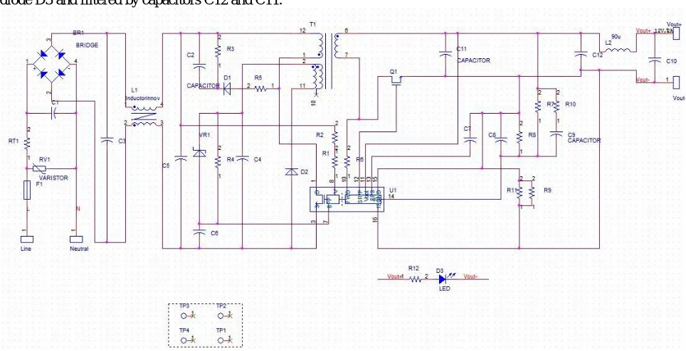
cycles are enabled, and at light load or no-load, most cycled are disabled orskipped. Once a cycle is enabled, the MOSFET will remain on until the primarycurrent ramps to the device current limit for the specific operating state. There arefour operating states (current limits) arranged such that the frequency content ofthe primary current switching pattern remains out of the audible range until at lightload where the transformer flux density and therefore audible noise generation is ata very low level. The secondary-side of the Inno-Switch- IC provides output voltage,output current sensing and drive to a MOSFET providing synchronous rectification.The secondary of the transformer is rectified by diode D3 and filtered by capacitors C12 and C11.
To reduce dissipation in the diode D3, synchronous rectification (SR) is provided by MOSFET Q1. The gate of Q1 is turned on by secondary-side controller inside IC U1, based on the winding voltage sensed via resistor R6 and fed into the FWD pin of the IC.In continuous conduction mode of operation, the MOSFET is turned off just prior to the secondary-side commanding a new switching cycle from the primary. In discontinuous mode of operation, the power MOSFET is turned off when the voltage drop across the MOSFET falls below a threshold of approximately 24 mV. Secondary-side control of the primary-side power MOSFET avoids any possibility of cross conduction of the two MOSFETs and provides extremely reliable synchronous rectification. As the SR MOSFET is not on for the full switching cycle, a small low current diode is still required (D3) for best in class efficiency. The secondary-side of the IC is self-powered from either the secondary winding forward voltage or the output voltage. Capacitor C7 connected to the BPS pin of Inno-Switch IC U1, provides decoupling for the internal circuitry. During CC operation, when the output voltage falls, the device will power itself from the secondary winding directly. During the on-time of the primary-side power MOSFET, the forward voltage thatappears across the secondary winding is used to charge the decoupling capacitor C7 via resistor R6 and an internal regulator. This allows output current regulation to be maintained down to ~10 V. Below this level the unit enters auto-restart until the output load is reduced.Output current issensed between theIS and GND pins with a threshold of approximately 33 mV to reducelosses. Once the current sense threshold is exceeded the device adjusts the number of switch pulses to maintain a fixed output current. During a fault condition such asshort-circuit of output, a large current will flow through the current sense resistors R9 and R11 due to discharge of the output capacitors C12 and C11 through the short-circuit. The output voltage is sensed via resistor divider R8 and R7. Output voltage is regulated so as to achieve a voltage of 1.265 V on the FEEDBACK pin. Resistor R10 and capacitor C9 form a phase lead network that ensure stable operation and minimize output voltage overshoot and undershoot during transient load conditions. Capacitor C8 provides noise filtering of the signal at the
the DC voltage across capacitor C5. At approximately 100 V DC, the current through these resistors exceeds the line under-voltage threshold, which results in enabling of U1. At approximately 435 VDC, the current through these resistors exceeds the line overvoltage threshold, which results in disabling of U1.
III.HARDWARE IMPLEMENTATION AND RESULTS
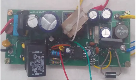
Hardware implementation of the proposed DC power supply using inno-switch is given in the figure 2.
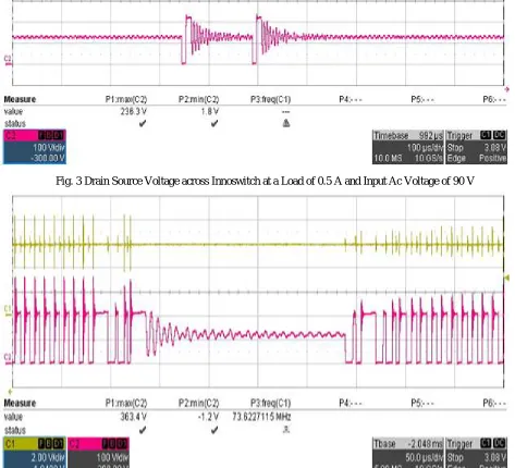
A prototype of the DC power supply using inno-switch has been built on a printed circuit board to verify the model. The input voltage was 85-264V ac. The output voltage was 12V. The full load current was 1A and the switching frequency was 100kHz. The results obtained from the hardware setup are given below. Figure 3&4 shows the drain source voltage across inno-switch at a load of 0.5A and input Ac voltage of 90& 220V respectively.
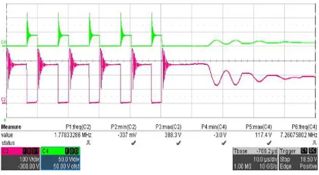
Figure 5&6 shows thedrain Source Voltage across Innoswitch and Synchronous Rectifier MOSFET at a Load of 0.5 A for input Ac Voltage of 220&90 V.
Fig. 3 Drain Source Voltage across Innoswitch at a Load of 0.5 A and Input Ac Voltage of 90 V
Fig. 5Drain Source Voltage across Innoswitch and Synchronous Rectifier MOSFET at a Load of 0.5 A for input Ac Voltage of 220 V
Fig.7 Drain Source Voltage across Inno-switch (Pink) and Transformer Primary current( Blue) at a Load of 0.5 A and Input Ac Voltage of 90 V
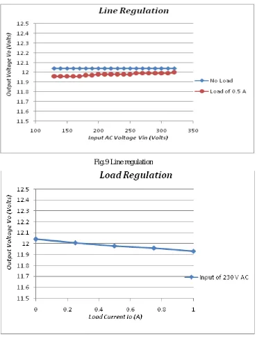
Figure 9&10 shows the line regulation& load regulation. Line regulation was plotted against output & input voltage. Load regulation was plotted against output voltage and load current.
Fig.9 Line regulation
IV. RESULT AND DISCUSSION
The proposed DC supply using inno- switch is shown in the figure 1 and its hardware setup is given in figure 2.Then we implement the hardware. The results obtained from the hardware setup of the DC supply using inno-switch are given in figures 3- 8.We also obtained the line and load regulation. The output designed for the proposed system is 12V.
V.CONCLUSION
An SMPS module based on isolated flyback topology was developed andtested for input AC Voltage range from 85 to 220 V. The Line Regulation and Load Regulation curves were obtained. The SMPS module was to have a reduced power delivering capability when load current is increased. This may be attributed to a higher value of primary inductance of the transformer and needs to investigated further. The effect of using RCD snubber in reducing the voltagespikes across the Inno-switch was also studied.
REFERENCES
[1] Y.F. Liu and P.C. Sen, "A General Unified Large Signal Model for Current Programmed DC-to-DC Converters," IEEE Transactions on Power Electronics, Vol. 9, No. 4, July 1994, pp. 414-424.
[2] R.D. Middlebrook, "Modeling Current-Programmed Buck and Boost Regulators," IEEE Transactions on Power Electronics, Vol. 4, January 1989, pp. 36-52.
.
[3] INN2603-2605 & INN2094 InnoSwitch-EP Family, product data sheet, Power Integrations, Inc., March. 2016.
[4] S.P. Hsu, A. Brown, L.Rensink and R.D. Middlebrook, "Modelling and Analysis of Switching DC-to-DC Converters in Constant-FrequencyCurrent-Programmed Mode," IEEE Power Electronics Specialists Conference (PESC), 1979, pp. 284-301.
[5]A. Soto, P. Alou, J. A. Cobos, and J. Uceda, "The Future DC-DC converter as an Enabler of Low Energy Consumption Systems with Dynamic Voltage Scaling," inProc. IEEE Ind. Electron. Conf., 2002, vol. 4, pp. 3244–3249.