MICROSTRIP PATCH ANTENNA ARRAY
DESIGN AND SIMULATION
Supriya Jaiswal
1, Haneet Rana
2,
Paurush Bhulania
3 1P G student. Amity School of Engg & Technology, Amity University, Noida , India,
2,3Department of Electronics & Communication , Amity School of Engg & Technology ,
Amity University , Noida , (India)
ABSTRACT
An antenna array is a collection of homogeneous antennas oriented similarly to get greater directivity and gain in a desired direction. This feature can be exploited to increase the gain of an antenna along with other important parameters, miniaturize classical antenna elements, and overcome some of the limitations of small antennas. In this paper a rectangular patch fed with microstrip feed line has been used to increase the bandwidth and multi resonant nature of the antenna array. The numerical study has been done by using Zeland make IE3D electromagnetic simulator.
Keywords:
Antenna Array, Antenna Gain, Slotted Microstrip Patch, IE3D Electromagnetic Simulator, Antenna Feed PointI. INTRODUCTION
The wireless industry is witnessing a volatile emergence today in present era. Today’s antenna systems demand
versatility and unobtrusiveness. Furthermore, aesthetics in the design of the systems are always important, some
applications require the antenna to be as miniaturized as possible. The basic drawbacks of patch antennas are
low bandwidth and comparable low gain even though these antennas are compact in size. In this paper we have
designed basic patch antenna operating for GSM and WLAN application and its array implementation to
enhance the subsequent Bandwidth and Gain and other related parameters such as Directivity, Antenna
efficiency etc.
II. MICROSTRIP PATCH ANTENNA
Microstrip patch antennas have a very high antenna quality factor (Q). It represents the losses associated with
the antenna where a large Q leads to narrow bandwidth and low efficiency. Q can be reduced by increasing the
thickness of the dielectric substrate. But as the thickness increases, an increasing fraction of the total power
delivered by the source goes into a surface wave. This surface wave contribution can be counted as an unwanted
power loss since it is ultimately scattered at the dielectric bends and causes degradation of the antenna
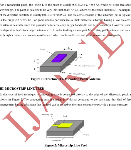
A Micro strip Patch antenna consists of a radiating patch on one side of a dielectric substrate which has a ground
plane on the other side as shown in Figure 1. The patch is generally made of conducting material such as copper
or gold and can take any possible shape. The radiating patch and the feed lines are usually photo etched on the
dielectric substrate.
For a rectangular patch, the length L of the patch is usually 0.3333λo< L < 0.5 λo, where λo is the free-space
wavelength. The patch is selected to be very thin such that t << λo (where t is the patch thickness). The height h
of the dielectric substrate is usually 0.003 λo≤h≤0.05 λo. The dielectric constant of the substrate (εr) is typically
in the range 2.2 ≤ εr≤ 12. For good antenna performance, a thick dielectric substrate having a low dielectric
constant is desirable since this provides better efficiency, larger bandwidth and better radiation. However, such a
configuration leads to a larger antenna size. In order to design a compact Micro strip patch antenna, substrates
with higher dielectric constants must be used which are less efficient and result in narrower bandwidth.
Figure 1: Structure of a Microstrip Patch Antenna
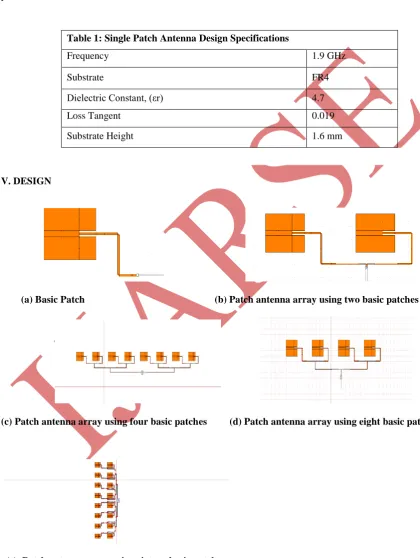
III. MICROSTRIP LINE FEED
In this type of feed technique, a conducting strip is connected directly to the edge of the Microstrip patch as
shown in Figure 2. The conducting strip is smaller in width as compared to the patch and this kind of feed
arrangement has the advantage that the feed can be etched on the same substrate to provide a planar structure.
.
Figure 2: Microstrip Line Feed
The purpose of the inset cut in the patch is to match the impedance of the feed line to the patch without the need
for any additional matching element. This is achieved by properly controlling the inset position. Hence this is an
easy feeding scheme, since it provides ease of fabrication and simplicity in modeling as well as impedance
IV. DESIGN SPECIFICATION OF MICROSTRIP FEED SLOTTED PATCH ANTENNA
Before designing the antenna, the first step is to consider the specification of the antenna based on its
application. After performing some research, the various parameters are listed in the Table 1, using the
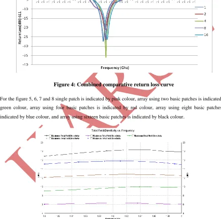
specifications we can design an array of microstrip antenna using two, four, eight, sixteen, thirty two basic
patches.
Table 1: Single Patch Antenna Design Specifications
Frequency 1.9 GHz
Substrate FR4
Dielectric Constant, (εr) 4.7
Loss Tangent 0.019
Substrate Height 1.6 mm
V. DESIGN
(a) Basic Patch (b) Patch antenna array using two basic patches
(c) Patch antenna array using four basic patches (d) Patch antenna array using eight basic patches
VI. RESULTS
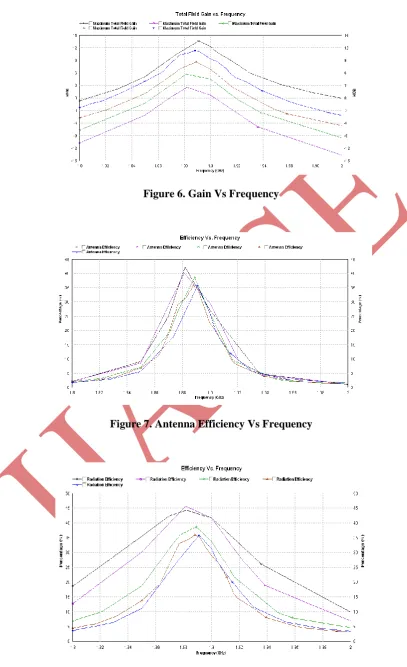
In this paper we show the results by comparing all the three proposed antennas along with array
implementation one by one on the basis of Directivity, Gain and Antenna Efficiency. It is quite clear
that while array implementation of same antenna the resonance remains invariant ,while other antenna
parameters improves for higher order of arrays.
Figure 4: Combined comparative return loss curve
For the figure 5, 6, 7 and 8 single patch is indicated by pink colour, array using two basic patches is indicated by
green colour, array using four basic patches is indicated by red colour, array using eight basic patches is
indicated by blue colour, and array using sixteen basic patches is indicated by black colour
.
Figure 6. Gain Vs Frequency
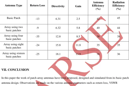
Quantitative analysis for all the designed geometries are given in table 2 below:-
Table 2 Antenna parameter comparison for Microstrip Feed Slotted Patch Antenna
Antenna Type Return Loss Directivity Gain
Antenna Efficiency (%) Radiation Efficiency (%)
Basic Patch -13 6.31 2.5 42 45
Array using two
basic patches -9 6.32 5.8 40 44
Array using four
basic patches -35 12.8 8.5 38 38
Array using eight
basic patches -24 15.8 11.8 35 35
Array using sixteen
basic patches -25 18.1 13.9 36 36
VII. CONCLUSION
In this paper the work of patch array antennas have been proposed, designed and simulated from its basic patch
antenna design. Observations are made on the various antenna parameters such as return loss, VSWR
Radiation pattern etc. in all the proposed cases. From the results of the simulation, it has been observed that the
influencing parameters of the antenna are as when we increase the number of array, the directivity, gain and
antenna efficiency increases accordingly. It is also noticeable that increment in some antenna parameter counter
balances other parameters.
VIII. REFERENCES
[1] Balanis C. A., 2005, “Antenna Theory: Analysis and Design”, 3rd ed. Hoboken, NJ: Wiley.
[2] Pozar D. M. and D. H. Schubert, 1995, “Microstrip Antennas—The Analysis and Design of Microstrip
Antennas and Arrays”. New York: IEEE Press,
[3] RameshGarg, Prakash Bhartia, Inder Bahl, Apisak Ittpiboon-2001 “Microstrip Antenna Design Handbook”
Artech House Publication
[4] M. Tariqul Islam, M.N. Shakib, N. Misran., and B. Yatim, “ Analysis of L-Probe Fed Slotted Microstrip
Patch Antenna,” in Eleventh IEEE International Conference on Communication Systems (IEEE ICCS 2008),
Guangzhou, China, November 19-21, 2008, pp. 380-383.
[5] “Design of microstrip patch antenna array” byY.K SINGH, S.GHOSH, IIT KHARAGPUR, IEEE.
[6] J. G. Vera-Dimas1, M. Tecpoyotl-Torres1, P. Vargas-Chable, J. A. Damián-Morales1, “Individual Patch
[7] “Design And Development Of Microstrip Patch Array Antenna” by Jagdish M. Rathod1, Yogesh P. Kosta2, Vipul , M.Dabhi3
[8] “Design, Analysis and Optimization of A Slotted Microstrip Patch Antenna Array at Frequency 5.25 GHz for WLAN-SDMA System” by Chandan Kumar Ghosh1 and Susanta Kumar Parui2International Journal on Electrical Engineering and Informatics - Volume 2, Number 2, 2010
[9] “Design Of A Microstrip Patch Antenna Array Using IE3D Software” by Y.K. Singh, S. Ghosh, K.Prathyush, Suyash Ranjan, Sagar Suthram, A. Chakrabarty, S. Sanyal