Sharif University of Technology
Scientia IranicaTransactions D: Computer Science & Engineering and Electrical Engineering www.scientiairanica.com
Tb/s all-optical nonlinear switching using SOA based
Mach-Zehnder interferometer
Y. Khorrami
a;, V. Ahmadi
aand M. Razaghi
ba. Department of Electrical and Computer Engineering, Tarbiat Modares University, Tehran, P.O. Box 14115-143, Iran. b. Department of Electrical and Computer Engineering, University of Kurdistan, Sanandaj, P.O. Box 416, Iran. Received 23 June 2012; received in revised form 29 October 2012; accepted 6 May 2013
KEYWORDS Ultrafast nonlinear optics;
All-optical devices; Switching;
Chirping; Mach-Zehnder interferometer; Semiconductor optical ampliers.
Abstract.A new method for increasing the speed of all-optical Mach-Zehnder Interfero-metric (MZI) switching with a bulk Semiconductor Optical Amplier (SOA), using chirped control signals, is suggested and theoretically analyzed. For 125fs input and chirped control pulses, we show acceleration of the gain recovery process using the cross phase modulation (XPM) eect. Our method depicts that Tb/s switching speeds, using bulk SOA-MZI with a proper Q-factor, is feasible. For the rst time, we reach operation capability at 2Tb/s with a Q-factor of more than 10. The new scheme also improves the extinction and amplitude ratio of the output power, as well as increasing the contrast ratio of the switched signal. We use a nite dierence beam propagation method for MZI analysis, taking into account all nonlinear eects of SOA, such as Group Velocity Dispersion (GVD), Kerr eect, Two Photon Absorption (TPA), Carrier Heating (CH) and Spectral Hole Burning (SHB).
c
2014 Sharif University of Technology. All rights reserved.
1. Introduction
High-speed optical communication networks with ter-abit transmission capabilities attract much attention, in terms of high capability and exibility in optical signal processing. Such ultrafast optical signal process-ing can be achieved usprocess-ing a Symmetric Mach Zehnder (SMZ) all optical switch family, including an origi-nal SMZ switch [1,2], a Delayed Interference Sigorigi-nal- Signal-wavelength Converter (DISC) [3], and a Polarization Discrimination SMZ (PD-SMZ) [4]. The Semiconduc-tor Optical Amplier (SOA) is a key element in many ultrafast switching schemes. The speed of switches based on SOA is limited, especially because of SOA carrier dynamics. To overcome this limitation, dierent approaches have been used. Wang et al. proposed and experimentally demonstrated a SOA based dierential
*. Corresponding author. Tel/Fax: +98 9190197109; E-mail addresses: [email protected] (Yaser Khorrami); v [email protected] (V. Ahmadi); [email protected] (M. Razaghi)
scheme at 40 Gb/s [5]. Bischo et al. suggested a new method using a XGM holding signal for increasing the speed of SOA-MZI converters to 160 Gb/s [6]. Nakamura et al. experimentally demonstrated a single channel OTDM, using a hybrid integrated SOA-MZI up to 168 GB/s [7-9]. Recently, Gutierrez suggested a new approach for all-optical signal processing using turbo-switched SOA-MZI at 160 Gb/s [10]. For bit rates higher than 168 Gb/s, data patterning eects are ob-served on the output signal, resulting in an increase in the probability of erroneous data detection. Repetition rates higher than 500 GB/s require a subpicosecond signal pulsewidth and the switching windows must approach the picosecond limit [1]. In these conditions, subpicosecond nonlinearities impose limitations on the switching structure. These limitations are attributed to inherent patterning eects associated with the gain recovery process in an SOA [6]. In this paper, we propose a new method for controlling the nonlinear phase dierence between MZI arms, using chirped control pulses. As a result of the frequency chirp imposed on an optical pulse, its spectrum is
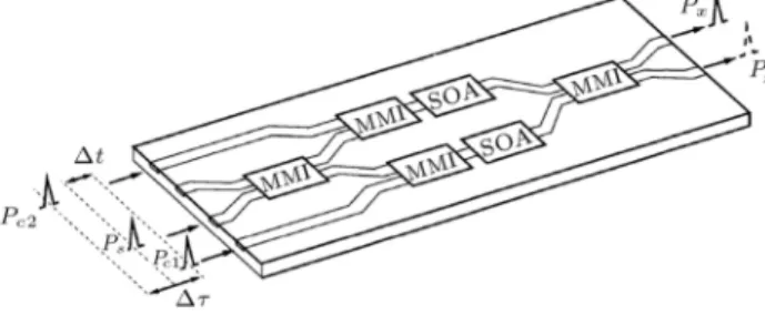
consider-Figure 1. Structure of monolithically integrated MZI switch with two SOA's and four multimode interference couplers (MMIs). Signal (Ps) and control pulses (Pc1; Pc2)
are used in the co-propagation arrangement.
ably broadened. On the other hand, unchirped pulses have the narrowest spectrum and are called transform-limited [11]. We show that the phase dierence between MZI arms can be equalized uniformly due to spectrum broadening, compared with an unchirped condition, which provides a better pattern quality factor.
2. SOA-MZI switch
In our study, all optical switch modeling consists of a symmetric MZI with two SOA located in the same relative position of each arm, as shown in Figure 1.
The data signal enters the structure and splits symmetrically into each arm by the rst multimode interference coupler (MMI). Two further control signals also are launched to each SOA via second and third couplers. The mechanism of switching is based on a time dierential between control pulses, so that the data signal is injected between two control pulses. Control 1, as shown in Figure 1, is presented in the lower arm and changes the refractive index of the lower SOA before the signal pulse enters. Control 2 is injected to the upper arm after the data signal and saturates the upper SOA. In the switched state, the control pulse, Pc1, saturates the lower SOA, inducing a
phase shift of 'NLbetween two arms, and a switched
data signal from bar (P=
out) to cross (Pout ) output port.
Control pulse, Pc2, switches back the SOA-MZI
from constructive to destructive interference and so resets the switch for the next set of pulses that arrive. Output power can be written as [1]:
P= out=P8in
n
G1+G2 2
p
G1G2cos('1 '2)
o ;
(1)
Pout =P8innG1+G2+2
p
G1G2cos('1 '2)
o ;
(2) 'NL(t)='1(t) '2(t)= (=2) ln(G2=G1):
(3) Pin(t) is input power and G1(t), '1, G2(t) and
'2 are the gain and phase dierences of SOA1 and
SOA2, respectively. 'NLis the total phase dierence
accumulated by the optical signals given by Eq. (3). is the linewidth enhancement factor associated with the gain changes due to carrier depletion and carrier heating. In the dierential scheme, the switching window width is determined by the time-delay between the two control pulses [1] as:
T==1
4 n
G1+ G2 2
p
G1G2cos('1 '2)
o ;
(4)
T=1
4 n
G1+ G2+ 2
p
G1G2cos('1 '2)
o :
(5)
3. Theoretical model
The following modied nonlinear Schrodinger equa-tion [12-14] is used for the analysis of SOAs and the characteristics of the switching scheme:
" @ @z
i 22
@2
@2+
2+
2P
2 +ib2
jV (; z)j2 #
V (; z)
= (
1 2gN()
1
f()+ iN
+12gT()(1 + iT) i12@g(; !)@! !0
@ @ 1
4
@2g(; !)
@!2 !0
@2
@2
)
V (; z); (6)
where:
gN() = g0exp
0 @ 1 Ws Z 1
e s=sjV (s)j2ds
1 A ; (7)
f() = 1 + 1
shbPshb +1
Z
1
u(s)e s=shbjV ( s)j2ds;
(8) gT()
= h1 +1
Z
1
u(s)e s=ch(1 e s=shb) jV ( s)j2ds;
h2 +1
Z
1
u(s)e s=ch(1 e s=shb) jV ( s)j4ds;
(9) @g(; !) @! !0
@2g(; !)
@!2
!0
= A2+ B2[g0 g(; !0)]; (11)
g(; !0) = gN(; !0)=f() + gT(; !0): (12)
A local time frame (= t z=vg) is introduced, which
propagates with group velocity, vg, at the center
fre-quency of an optical pulse. The slowly varying envelope approximation is used in Eq. (4). Here, V (; z) is the time domain complex envelope function of an optical pulse, jV (; z)j2corresponds to the optical power, 2is
The Group Velocity Dispersion (GVD), is linear loss, 2P is the Two-Photon Absorption (TPA) coecient,
b2(= !0n2=cA) is the instantaneous Self-Phase
Modu-lation (SPM) term, due to the instantaneous nonlinear Kerr eect (n2), !0(= 2f0) is the center angular
frequency of the pulse, c is the velocity of light in a vacuum, A is the eective area of the active region, gN() is the saturated gain due to carrier depletion,
g0 is the linear gain, Ws is the saturation energy, sis
the carrier lifetime, f() is the SHB function, Pshb is
the SHB saturation power, shb is the SHB relaxation
time, Nand T are the linewidth enhancement factors
associated with gain changes, due to carrier depletion and Carrier Heating (CH), gT() is the resulting
gain change due to CH and TPA, u(s) is the unit step function, CH is the CH relaxation time, h1 is
the contribution of stimulated emission and free carrier absorption to CH gain reduction, h2is the contribution
of TPA, A1 and A2 are the slope and curvature of
linear gain at !0, and B1 and B2 are constants. The
gain spectrum of an SOA can be approximated by the following second-order Taylor expansion in !:
g(; !) =g(; !0) + !@g(; !)@! !0
+(!)2 2
@2g(; !)
@!2 !0: (13)
The time derivative terms in the modied nonlinear Schrodinger equation are replaced with the central-dierence approximation in order to solve the equation by the FD-BPM [12]. The parameters used in the simulation are listed in Table 1 [1,15].
4. Simulation results and discussion
Our numerical model is compared with Bischo's results [16] in Figure 2. SOA's injection current
Table 1. The parameters used in simulation [1,15].
Symbol Quantity Values (units)
L SOA Length 500 m
A Eective area 5 m2
f0 Center frequency of the pulse 193.5 THz
g0 Linear gain 120 cm 1
2 Group velocity dispersion 0.045 ps2cm 1
Ws Saturation energy 10 pj
N Linewidth enhancement factor due to the carrier depletion 7
T Linewidth enhancement factor due to CH 1
h1 The contribution of stimulated emission and free
carrier absorption to the carrier heating gain reduction 0.3 cm
1pj 1
h2 The contribution of TPA 300 fs cm 1pj 2
s Carrier lifetime 650 ps
CH Carrier heating relaxation time 800 fs
SHB SHB relaxation time 150 fs
PSHB SHB relaxation power 11.32 W
Linear loss 15 cm 1
n2 Instantaneous nonlinear Kerr eect -0.6 cm2TW 1
2P TPA coecient 1.6 cm 1W 1
A1
Parameters describing second order Taylor expansion of the dynamically gain spectrum
0.8 fs m 1
A2 -150 fs
B1 -150 fs2m 1
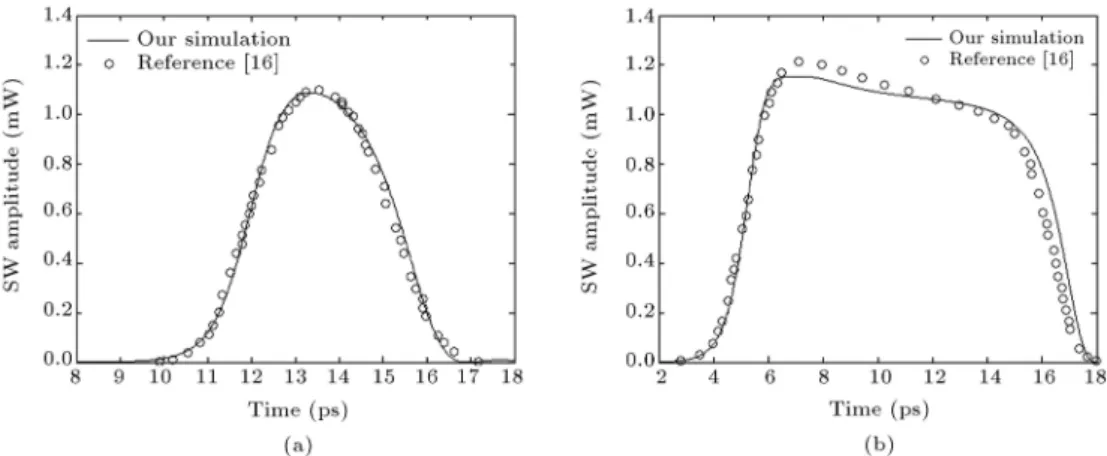
Figure 2. Switching Window (SW) amplitude versus time. SWs are shown for time-delay() of (a) 4 ps and (b) 12 ps between the control pulses.
is 66.5mA and the input pulse Full Width at Half Maximum (FWHM) is 2 ps. The remaining parameters are the same as [16]. As shown in Figure 2, there is good agreement between our results and those in [16], according to two dierent time-delays, equal to 4ps and 12ps, in the switching window.
We consider the co-propagation state, which re-veals a better performance regarding its small switch-ing window and high ON/OFF ratio, while, in counter propagation, the switching window is larger [17,18]. Thus, for high speed applications, the co-propagation scheme is more reliable.
Based on the structure shown in Figure 1, Gaus-sian pulses with FWHM of 125 fs and pulse energy of 0.01 fJ, 18 fJ and 16 fJ are considered for signal and control pulses (Ps, Pc1 and Pc2), respectively. Control
pulses are launched with = 0:3 ps delay to the switch.
Figure 3 depicts the time response of the inte-grated SOA MZI switch under unchirped and chirped control pulse conditions with 2 Tb/s input data signal and 0.5 Tb/s control pulse. Simulations are performed for two conditions of unchirped and chirped control pulses, but the input data pulse remains unchirped in all calculations. Figure 3(a) shows the MZI switching dynamics for a data pulse rate of 2Tb/s and a control pulse rate of 0.5 Tb/s, before and after each selected data pulse. In this case, data input pulse energy is chosen very low for preventing SOA's gain saturation by data pulse injection. Figure 3(b) and (c) show the switched output power for unchirped and chirped states, respectively.
Figure 3(b) shows the degradation of the switched pulse power because of the high carrier depletion rate of SOAs. Figure 3(c) shows the MZI output power for chirped Gaussian control pulses with a chirped factor of -5.
As observed, there is a considerable attenuation of peak patterns on the output switched power in Figure 3(b) as compared with Figure 3(c).
Figure 3. (a) 2 Tb/s input data signal and 0.5 Tb/s control pulses to the integrated SOA MZI switch. (b) Resulting MZI output power with unchirped control pulses, and (c) with chirped control pulses. Chirp factor is -5. Time delay between control pulses is 0.3 ps. The energy of input data pulse, control 1 and control 2 is 0.01 fJ, 18 fJ and 16 fJ, respectively.
To investigate this phenomenon, we analyze the SOA performance on each arm, as follows.
For Gaussian pulses with chirp factor of C, we use the following equation [11]:
A(0; t) = A0exp 1 + iC2
t T0
2!
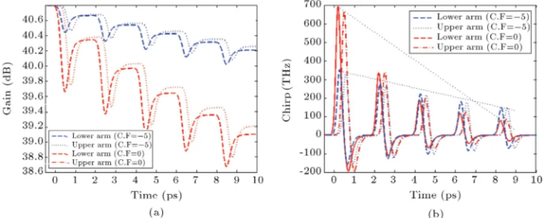
Figure 4. (a) Gain variation of each MZI arms with time. Upper arm has chirp factor of -5 and lower is unchirped. Carrier depletion rate reduces with adding negative chirp to control pulses. (b) Chirp variation of each MZI arms with time in two state of chirped and unchirped state for each control pulse.
Figure 5. (a) Normalized phase dierence between two arms of MZI. Phase variation is almost xed for chirped state. (b) Variation of switching window with time. SW amplitude uctuation is lower for chirped state.
where the parameter, C, represents the frequency chirp imposed on the pulse. A0 is the peak amplitude and
T0 is the half-width at 1=e intensity point [11]. In all
the following results, C = 5, is a xed chirp factor. Figure 4(a) shows the variation of MZI nonlinear gain in each arm. As shown, for the unchirped state, increasing gain recovery time after some switching processes leads to a patterning eect.
The chirped control pulses result in a lower amount of gain saturation, thus, reducing the output patterning eect compared to schemes with unchirped control pulses. The idea of using chirped control pulses temporarily equalizes the total power injected into the SOA's, thereby, reducing the patterning eect. As seen in Figure 4(a), injection of chirped control pulses reduces the SOA carrier depletion rate, resulting in a reduction of the gain (and also refractive index) changes induced by unchirped control pulses. It must be recognized that the recovery time of the SOAs takes place in a few ps and, therefore, the next bit cannot be processed until the SOAs are recovered. This poses a major limitation on application of a device without chirp injection.
Figure 4(b) shows the chirp variation of each MZI arm for chirped and unchirped control pulses. The results show the reduction of total chirp by each SOA in comparison to the unchirped state. Note that this reduction is noticeable for the rst and second switched symbols, but for later ones, we have increments of chirp in both negative and positive chirp sections. This behavior obviously shows that for chirped control pulses, the slope of the chirp (shown by the dotted line in Figure 4(b)) is lower than that in the unchirped state. For more investigation, we calculated the phase dierence and Switching Window (SW) amplitude variations versus the time in Figure 5.
Figure 5(a) shows the phase dierence between two arms of MZI. Slower changes of phase dierence on each switched symbol can reduce output patterning for the chirped state in comparison with the unchirped state. Figure 5(b) shows the amplitude of switching window as a function of time. In contrast, the uctua-tion of SW amplitude for a chirped state is higher than for an unchirped state. As shown in Figure 4(b), in the presence of chirped control pulses, chirp variation becomes stable. As illustrated in Figure 5(a), the same
Figure 6. The optical eye diagram of MZI switch for 2Tb/s data rate for both (a) unchirped and (b) chirped states.
phenomena occurred for the dierential phase in this case, which in turn leads to enhanced SW amplitude, as can be seen in Figure 5(b).
As a next step, we compare the eye diagram of each state. Figure 6(a) shows the eye diagram of the unchirped state, which is gradually closing due to the pattern eect, but which, for chirped control pulses, enhances system performance, based on Figure 6(b).
For performance evolution, we use four main pa-rameters of switch over the output eye diagram. These are Fluctuation in the Mark Power Level (FMPL), Contrast Ratio (CR), Extinction Ratio (ER) and Qual-ity factor (Q). These parameters are dened as [6,19-21]:
FMPL =Pmax1
P1
min; (15)
CR =Pmean1
P0
mean; (16)
ER = Pmin1
P0
max; (17)
Q = Pmean1 1+ P0mean0 ; (18)
where P1
max, Pmin1 and Pmax0 , Pmin0 are the maximum
and minimum values of the peak power of \1" and \0", respectively. P1
meanand Pmean0 are the average power of
output signals \1" and \0", and 1and 2are standard
deviations of all \1" and \0". Figure 6(a) shows the unchirped state with FMPL, CR, ER and Q of 3.7, 6.51, 15.42 and 2.12, respectively. Figure 6(b) shows output switched signals with chirped control pulses (C = 5) and 0.6, 10.55, 16.6 and 10.7, as switch parameters equal to FMPL, CR, ER and Q, respectively. As seen, in the chirpy form, we have much better quality for switch factors. In this situation, the pattern eect becomes less and the eye pattern is clearly open with a Q of 10.7, in comparison with the unchirped state,
by a Q-factor of 2.12. Therefore, the recovery process is much faster for chirped states compared to case in which no chirp is applied to the switch.
In order to test the inuence of the switching window width on the MZI switching behavior, we investigate the eect of time delay variation between two control pulses.
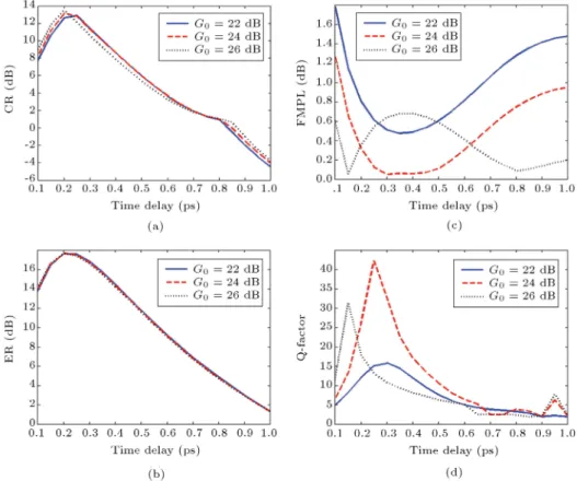
Figure 7 depicts the variation of four basic switch parameters (CR, ER, FMPL and Q-factor) with varia-tion of delay time between two control pulses.
The curves are given for three dierent unsatu-rated gain (G0 = exp(g0L)) values equal to 22 dB,
24 dB and 26 dB in order to demonstrate the impact of linear gain g0, and, equivalently, switch current on
the output quality. The switch current for each SOA can be written as [22]:
I =
g0
aN0 + 1
I0; (19)
where is connement factor, is dierential gain, and I0and N0are current and carrier density required
for transparency, respectively. Taking G0 instead of
I gives freedom for experimental work, and one can change structural parameters to reach a specic g0.
We obtain maximum CR, ER, Q and minimum FMPL for a time delay of around 0.2 ps, as shown in Figure 7. In Figure 7(a) and (b), we see same variations of CR and ER for every three amounts of G0.
Furthermore, as time delay decreases, our proposed scheme results are enhanced. Moreover, as depicted in Figure 7, for > 0:25, CR and ER degrade when the time delay is increased, whilst the opposite occurs for the FMPL in Figure 7(c), so that FMPL has minimum points in the time delay of 0.4 when the unsaturated gains become 22 dB and 24 dB. FMPL curvature for G0= 26 dB has two relative minimum points in time
delays of 0.15 ps and 0.82 ps in which 0.15 ps is the absolute minimum point. As seen, unsaturated gain variation does not imply sensitive dierences on CR and ER, as shown in Figure 7(a) and (b).
Figure 7. Variation of (a) CR, (b) ER, (c) FMPL and (d) Q-factor of switch with time delay between two control pulses for three dierent values of G0 equal with 22, 24 and 26 dB.
The optimum Q-factor of the switch is shown for G0 of 24 dB around 0.25 ps in Figure 7(d). Generally,
larger time delay leads to lower Q-factor because of the decrease in the overlapping of two neighboring control pulses with the data pulse. Therefore, for larger time delay, the eect of chirp gradually decreases on the data switching mechanism. Figure 7 depicts that the best time delay is around 0.25 ps for G0 of 24 dB.
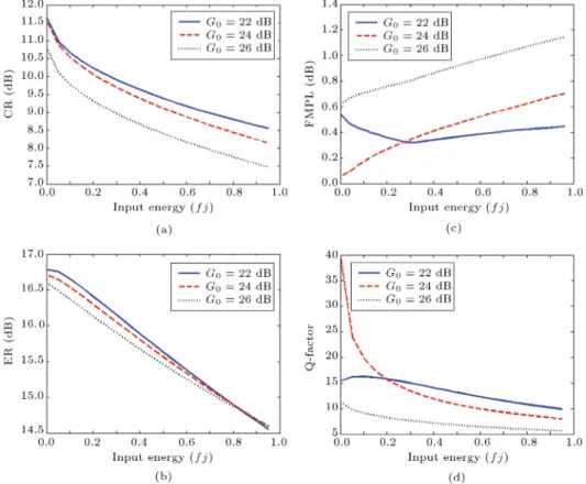
Figure 8 displays the variation of switch parame-ters with the input data energy for dierent values of unsaturated gain. As before, we use chirped control pulses of C = 5, and 18 fJ and 16 fJ pulse energy for the rst and second control pulses, respectively.
Figure 8(a) and (b) reveal that CR and ER degrade when the input data pulse energy is increased. Figure 8(c) shows that FMPL becomes larger as unsaturated gain increased. For G0 = 24 dB, as
illustrated in Figure 8(c) and (d), and input energies lower than 0.1 fJ, FMPL and Q-factor have minimum and maximum values, respectively. However, all switch parameters can be improved by decreasing the data pulse energy. For lower amounts of input data pulse energy, the eect of input data pulse energy on SOA saturation is eliminated and, therefore, the phase dierence between the two arms is only adjusted with the energy of the chirped control pulses. Higher data energy imposes extra gain saturation on both MZI arms. Increases of input energy can saturate SOA
gain and this increases the unwanted switching rate for unexpected symbols. Thus, for higher values of input data pulse energy, we obtain far from ideal amounts of switch parameters, as seen in Figure 8(a) and (d).
To become clearer, we investigate chirp factor variation on switch output patterns. Figure 9 depicts the variation of four basic parameters (CR, ER, FMPL and Q-factor), with variations of the chirp factor of chirped control pulses, for three values of unsaturated gains of 22 dB, 24 dB and 26 dB. Figure 9 depicts that switch parameters are sensitive to the chirp of control pulses, so, an increase in the control chirp factor can slow down the carrier depletion rate in each arm and, therefore, gain recovery time decreases. Figure 9(a) and (b) show that for G0 = 22 dB, there are better
amounts of CR and ER. An increase of G0 shows a
higher rate of carrier depletion. Then, for lower values of G0, as seen in Figure 9(a) and (d), better CR,
ER, FMPL and Q-factor can be achieved not only in chirped, but also in unchirped approaches. Figure 9(d) depicts that the best Q-factor for positive chirp can be achieved in comparison with negative chirp.
Similarly, we can see this phenomenon in Fig-ure 9(a) for positive chirp factors. The opening rate of the eye diagram for positive chirp is more than for the negative chirp, resulting in better values of Q-factor on positive chirp, as shown in Figure 9(d). By this illustration, we want to come back to Figure 4(b).
Figure 8. Variation of (a) CR, (b) ER, (c) FMPL, and (d) Q-factor with variation of input data energy for three dierent value of G0 equal with 22, 24 and 26 dB.
Figure 9. Variation of (a) CR, (b) ER, (c) FMPL, and (d) Q-factor with variation of chirp factor for three dierent value of G0 equal with 22 dB, 24 dB and 26 dB. Input data energy, control 1 and 2 energies are 0.01 fJ, 18 fJ and 16 fJ,
Figure 4(b) shows that for the negative chirp factor of control pulses, the slope of the dotted line is lower than the slope for the unchirped state. Similarly, for positive chirp factors, this slope becomes lower, in comparison with negative chirp factors. Therefore, more equalization can be found for the carrier depletion rate of positive chirp factors compared to negative ones. Figure 9(d) shows the best Q-factor for the chirp factor of +3 for G0= 22 dB. Furthermore, Figure 9(d)
depicts that for positive chirps around +3, lower values of G0 give a better Q-factor, whilst, in Figures 7(d)
and 8(d), the best Q-factor takes place for higher amounts of unsaturated gain. This shows that chirp factor variation not only changes the Q-factor, but can also improve the output characteristics of the proposed scheme by selecting the proper unsaturated gain.
5. Conclusion
To achieve very high speed all-optical switching, for the rst time, we use chirped control pulses as push-pull signals in a deferential symmetric MZI switching structure. Reduction of carrier depletion and gain saturation, and equalization of experienced chirp and phase dierences in each MZI arm are the results of using chirped control pulses. Furthermore, this equalization is higher for positive chirp factors, further reducing the pattern eect in output switched pulses. Eye diagrams for two dierent chirped and unchirped states proved that the recovery process of each SOA can be improved for reaching quality factors higher than 10. We investigated the impact of data input energy, the time delay between two control pulses, and unsaturated gain, on basic parameters of the MZI switch. Our results show that femtosecond switching with higher eciency is still possible using bulk SOAs.
Supper Gaussian pulses can be used for more in-vestigation, because such pulses broaden more rapidly than Gaussian pulses. Therefore, super Gaussian chirped control pulses may be better candidates for future research on dierential MZI switches.
Acknowledgement
This work is supported by Iran Telecommunication Research Center (ITRC).
References
1. Schreieck, R.P., Kwakernaak, M.H., Jackel, H. and Melchior, H. \All-optical switching at multi-100-Gb/s data rates with Mach-Zehnder interferometer switches", IEEE J. of Quantum Electron, 38, pp. 1053-1061 (2002).
2. Nakamura, S., Ueno, Y. and Tajima, K. \Femtosecond switching with semiconductor-optical-amplier-based
symmetric Mach-Zehnder-type all-optical switch", J. of Appl. Phys. Lett., 78, pp. 3929-3931 (2001). 3. Ueno, Y., Nakamura, S., Tajima, K. and Kitamura, S.
\3.8-THz wavelength conversion of picosecond pulse using a semiconductor delayed-interference signal-wavelength converter (DISC)", IEEE Photon. Technol. Lett., 10, pp. 346-348 (1998).
4. Tajima, K., Nakamura, S. and Sugimoto, Y. \Ultrafast polarization-discriminating Mach-Zehnder all-optical switch", Appl. Phys. Lett., 67, pp. 3709-3711 (1995). 5. Wang, Q., Zhu, G., Chen, H., Jaques, J., Leuthold,
J., Piccirilli, A.B. and Dutta, N.K. \Study of all-optical XOR using Mach-Zehnder interferometer and dierential scheme", IEEE J. of Quantum Electron, 40, pp. 703-710 (2004).
6. Bischo, S., Nielsen, M.L. and Mork, J. \Improving the all-optical response of SOAs using a modulated holding signal", J. of Lightwave. Technol., 22, pp. 1303-1308 (2004).
7. Nakamura, S., Ueno, Y., Tajima, K., Sasaki, J., Sugimoto, T., Kato, T., Shimoda, T., Itoh, M., Hatakeyama, H., Tamanuki, T. and Sasaki, T. \Demultiplexing of 168-Gb/s data pulses with a hybrid-integrated symmetric Mach-Zehnder all-optical switch", IEEE Photon. Technol. Lett., 12, pp. 425-427 (2000).
8. Nakamura, S., Ueno, Y. and Tajima, K. \168-Gb/s all-optical wavelength conversion with a symmetric-Mach-Zehnder-type switch", IEEE Photon. Technol. Lett., 13, pp. 1091-1093 (2001).
9. Tajima, K., Nakamura, S. and Ueno, Y. \Ultrafast all-optical signal processing with symmetric Mach-Zehnder type all-optical switches", Optical and Quan-tum Electronics, 33, pp. 875-897 (2001).
10. Gutierrez, R. \Turbo-switched Mach-Zehnder inter-ferometer performance as all-optical signal processing element at 160 Gb/s", Optics Communications, 282, pp. 4345-4352 (2009).
11. Agrawal, G.P., Fiber Optic Communication Systems, Ed., 3th Edn., John Wiley Series in Microwave and Optical Engineering (2002).
12. Das, N.K., Yamayoshi, Y. and Kawaguchi, H. \Anal-ysis of basic four-wave mixing characteristics in a semiconductor optical amplier by the nite-dierence beam propagation method", IEEE J. of Quantum Electron, 36, p. 1184 (2000).
13. Das, N.K., Kawazoe, T., Yamayoshi, Y. and Kawaguchi, H. \Analysis of optical phase-conjugate characteristics of picosecond four-wave mixing signals in semiconductor optical ampliers", IEEE J. of Quan-tum Electron, 37, pp. 55-62 (2001).
14. Razaghi, M., Ahmadi, V. and Connelly, M. \Compre-hensive nite-dierence time-dependent beam propa-gation model of counterpropagating picosecond pulses in a semiconductor optical amplier", IEEE J. of Lightwave Technology, 27, pp. 3162-3174 (2009).
15. Kao, Y.H., Goltser, I.V., Jiang, M., Islam, M.N. and Raybon, G. \Gain dispersion induced subpicosecond pulse breakup in a ber and semiconductor laser amplier combined system", Appl. Phys. Lett., 27, pp. 4221-4223 (1996).
16. Bischo, S., Buxens, A., Fischer, St., Dulk, M., Clausen, A.T., Poulsen, H.N. and Mrk, J. \Compar-ison of all-optical co- and counter-propagating high-speed signal processing in SOA-based Mach-Zehnder interferometers", Optical and Quantum Electronics, 33, pp. 907-926 (2001).
17. Kang, K.I., Chang, T.G., Glesk, I. and Prucnal, P.R. \Comparison of Sagnac and Mach-Zehnder ultrafast all-optical interferometric switches based on a semi-conductor resonant optical nonlinearity", Appl. Optics, 35, pp. 417-426 (1996).
18. Toliver, P., Runser, R., Glesk, I. and Prucnal, P. \Comparison of Sagnac and Mach-Zehnder ultrafast all-optical interferometric switches based on a semi-conductor resonant nonlinearity", Conf. on Lasers and Electro Optics, pp. 254-255 (2000).
19. Sun, H., Wang, Q., Dong, H., Chen, Z., Dutta, N.K., Jaques, J. and Piccirilli, A.B. \All-optical logic XOR gate at 80 Gb/s using SOA-MZI-DI", IEEE J. of Quantum Electronics, 42, pp. 747-751(2006).
20. Taraphdar, C., Chattopadhyay, T. and Roy, J.N. \Mach-Zehnder interferometer-based all-optical re-versible logic gate", Optics and Laser Technology, 42, pp. 249-259 (2010).
21. Chattopadhyay, T. and Roy, J.N. \Semiconductor optical amplier (SOA) - assisted Sagnac switch for designing of all-optical tri-state logic gates", J. of Light and Electron Optics, 12, pp. 1073-1078 (2011). 22. Agrawal G.P. and Olsson, N.A. \Self-phase modulation
and spectral broadening of optical pulses in semicon-ductor laser ampliers", IEEE J. of Quantum Electron, 25, pp. 2297-2306 (1989).
Biographies
Yaser Khorrami received his BS degree in Electronics Engineering from Kashan University, Kashan, Iran, in
2005, and an MS degree in Electrical Engineering from Tarbiat Modares University, Tehran, Iran, in 2011. He is, currently, working at the Iranian Space Agency (ISA), Tehran, Iran. His research interests include simulation and investigation of semiconductor optical ampliers (SOA) in Mach Zehnder Interferometers.
He is also working on the Schrodinger equation for taking into account all nonlinear eects of the SOA-waveguide, such as Two Photon Absorption (TPA), Spectral Hole Burning (SHB), Carrier Heating (CH), Carrier Depletion (CD), Self-Phase Modulation (SPM), cross phase modulation (XPM), saturation energy ef-fect and other eective parameters, like the Kerr eect. He has published and presented a number of papers at international conferences on Optics and Photonics. Vahid Ahmadi received his BS degree in Electron-ics Engineering from Sharif University of Technology, Tehran, Iran, in 1986, an MS degree in Electrical Engi-neering from Tarbiat Modares University, Tehran, Iran, in 1990, and a PhD degree in Electrical Engineering from Kyoto University, Kyoto, Japan, in 1994. He is, currently, Professor in the Department of Electrical and Computer Engineering at the University of Tarbiat Modares, Tehran, Iran. He is a regular reviewer of several international technical journals and conference papers in the area of optical communications and photonic devices.
Mohammad Razaghi received a BS degree in Elec-tronics Engineering from Razi University, Kermanshah, Iran, in 2001, and MS and PhD degrees in the same subject from Tarbiat Modares University, Tehran, Iran, in 2003 and 2009, respectively. He is, currently, Assistant Professor in the Department of Electrical and Computer Engineering at the University of Kurdistan, Sanandaj, Iran.
He is member of IEEE, and Deputy Chairman of the West Branch Iranian Association of Electrical and Electronics Engineers (IAEEE). He is a regular reviewer of several international technical journals and conference papers in the area of optical communica-tions and photonic devices.
![Table 1. The parameters used in simulation [1,15].](https://thumb-us.123doks.com/thumbv2/123dok_us/8390501.2229364/3.892.180.734.626.1154/table-the-parameters-used-in-simulation.webp)

![MD5 considered harmful today [vangelis] pdf](data:image/gif;base64,R0lGODlhAQABAIAAAP///wAAACH5BAEAAAAALAAAAAABAAEAAAICRAEAOw==)