Fundamentals
of
Electrical
and
Electronics
Engineering
Laboratory
Manual
School of Engineering
ECE
Department
G
D
Goenka
University
Gurgaon, Haryana
Name:
Roll Number:
Section/Group:
The document is for internal circulation only.
Copyright © 2013 G D Goenka University. All rights reserved.
All materials on these pages are copyrighted by the G D Goenka University. All rights reserved. Reproduction, modification, retransmission, in any form or by any means, electronic, mechanical or otherwise, for reasons other than personal use, is strictly prohibited without prior written permission.
First Edition September, 2013
Published by:
SCHOOL OF ENGINEERING
Department of Electronics and Communication
Engineering
G
D
Goenka
University
PREFACE
The
School
of
Engineering
(SoE),
GDGU
has
prepared
this
laboratory
manual.
It
is
designed
as
an
instruction
book
for
purposes
listed
in
order
of
importance
as
follows:
1.
To
provide
techniques,
procedures
and
precautions
related
to
the
experiments.
2.
To
provide
the
laboratory
safety
and
general
rules
and
instructions.
3.
To
provide
a
general
reference
book
that
will
give
information
which
will
assist
in
the
understanding
of
details
about
the
laboratory
and
the
experiment
to
be
performed.
The
manual
is
prepared
with
the
idea
that
the
revisions
must
be
made
periodically
in
order
to
have
the
available
text
that
represents
the
experiments.
It
has
been
tried
to
maintain
the
format
with
diagrams,
tables
and
illustrations.
It
is
believed
that
the
information
in
the
manual
will
enhance
the
practical
skills
of
the
students
along
with
developing
the
base
of
the
subject.
Any
suggestions
and
comments
for
further
improvement
of
this
manual
will
be
gratefully
acknowledged.
Authors
Mandeep Narula
Anita Jindal
Akanksha Sharma
G D Goenka University, Gurgaon
General
Rules
and
Instructions:
To complete all the experiments within time, to understand them completely and to make laboratory experiments safe and effective, each student must obey the following points:
1. General discipline in the Lab
• Students must turn up in time and contact concerned faculty for the experiment they are supposed to perform
• Students will not be allowed after ten minutes from the scheduled time
• Students will not leave the lab till the period is over
• Attendance in the lab class is compulsory. As an incentive, certain percentage of lab marks is allotted for attendance in the internal evaluation of lab performance.
• Each group of students must write a satisfactory report for each lab experiments in order to pass the course
• Students should come prepared for their experiment with lab manual
• Experimental results should be entered in the lab manual and certified/signed by concerned faculty
• Students must get the connection of the experimental setup verified before switching on the power supply
• After the experiment is over, the experimental kits/modules. DMM and any other tools issued for the experiments should be returned to the lab instructor
• Students should not unnecessarily fiddle with the instruments knob or any other pot. in the instruments which may disturb the calibration accuracy, range or zero etc.
• Students should maintain silence while performing the experiments. Should any necessity arises for discussion amongst them, they should discuss with a very low pitch without disturbing the adjacent groups
• Students should not attend a different lab group/section other than the one assigned at the beginning of the session
FEEE
5 | P a g e
2. Preparations and Performance
Students should come to the lab thoroughly prepared on the experiments they are assigned to perform on that day
Faculty may check their preparation and understanding of the experiments. If not found satisfactory, students may be debarred from doing the experiments
Students should record the experimental results and observation in the lab manual
Students must bring the lab manual on each practical class with written records of the last experiments performed complete in all respect
Students without lab manual will not be allowed to do the experiments and hence loose their attendance
Any instrument damaged or tools lost during experiments may attract punishment in the form of fine or suspension from the class
3. Lab Report
Each student is required to write a complete report of the experiment he has performed and bring to lab class for evaluation in the next working lab
Report should be written very clearly and lab record should be maintained neatly
The lab report must contain the following:
i. Duly completed title page ii. Graphs/Waveforms iii. Observation Table iv. Result
FEEE
6 | P a g e
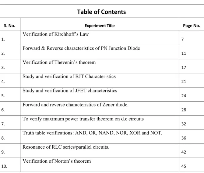
Table
of
Contents
S. No. Experiment Title Page No.
1.
Verification of Kirchhoff’s Law
7
2.
Forward & Reverse characteristics of PN Junction Diode
11
3. Verification of Thevenin’s theorem
17
4.
Study and verification of BJT Characteristics
21
5.
Study and verification of JFET characteristics
24
6. Forward and reverse characteristics of Zener diode.
28
7.
To verify maximum power transfer theorem on d.c circuits
32
8.
Truth table verifications: AND, OR, NAND, NOR, XOR and NOT.
36
9. Resonance of RLC series/parallel circuits.
42
10.
Verification of Norton’s theorem
45
FEEE
7 | P a g e
Experiment 1
Date of Performance__________ Date of Submission ____________Faculty’s Signature ______________
Aim:
Verification of Kirchhoff’s Law
Equipment:
Bread Board, Multimeter, Resistors (1 Kohm (2), 1.2 kohm (2), 2.4 kohm), Power Supply and connecting wires
Theory:
Kirchhoff’s Voltage Law states that the algebraic sum of all the voltages around any closed path (loop or mesh) is zero.
Applying Kirchhoff’s voltage law to the first and the second loops in the circuit shown in Figure 1 yields:
Loop 1: -Vs +V1 +V2 +V5 = 0 (1a) Loop 2: -V2 +V3 +V4 = 0 (1b)
Figure 1
Kirchhoff’s Current Law states that the algebraic sum of all the currents at any node is zero.
Applying Kirchhoff’s current law to the first four nodes in the circuit shown in Figure1 yields the following equations;
Node a: -Is + I1 = 0 (2a) Node b: -I1 + I2 + I3 = 0 (2b) Node c: -I3 + I4 = 0 (2c) Node d: -I2 - I4 + I5 = 0 (2d)
Procedure:
1. Construct the circuit shown in Figure 1 using the values below: R1 = 1 Kohm
R2 = 2.4 Kohm
FEEE
8 | P a g e
R4 = 1 Kohm R5 = 1.2 Kohm
2. Set the Variable Power Supply (Vs) to 5 Volts.
3. Accurately measure all voltages and currents in the circuit using the Digital Multi-Meter (DMM). 4. Record the measurements in a tabular form containing the measured voltage and current values as shown below:
Branch V [Volts] I [mA] R [kohm]
V1, I1 V2, I2 V3, I3 V4, I4 V5, I5 Vs, Is
5. Verify KVL for the loops in the circuit using equations 1a and 1b.
6. Verify KCL for the nodes in the circuit using equations 2a, 2b, 2c and 2d.
Precautions:
1. Connect voltmeter and Ammeter in correct polarities as shown in the circuit diagram.
2. Do not switch ON the power supply unless you have checked the circuit connections as per the circuit diagram
Result:
FEEE
9 | P a g e
Questions for Lab Report:
1. Theoretically calculate the voltages and currents for each element in the circuit and compare them to the measured values.
FEEE
10 | P a g e
Questions:
1. What is the statement of kirchhoff’s first law?
2. What is the internal resistance of the ideal voltage source?
3. What is the internal resistance of the current source ideally?
4. What is the active network?
FEEE
11 | P a g e
Experiment 2
Date of Performance__________ Date of Submission ____________Faculty’s Signature ______________
Aim:
Forward & Reverse characteristics of PN Junction Diode
Equipment:
Bread Board, Multimeter, PN Junction Diode IN4001, Resistor (1kohm), Power Supply and connecting wires
Theory:
Donor impurities (pentavalent) are introduced into one-side and acceptor impurities into the other side of a single crystal of an intrinsic semiconductor to form a p-n diode with a junction called depletion region (this region is depleted off the charge carriers). This region gives rise to a potential barrier Vγ called Cut- in Voltage. This is the voltage across the diode at which it starts conducting. The P-N junction can conduct beyond this Potential.
The P-N junction supports uni-directional current flow. If +ve terminal of the input supply is connected to anode (P-side) and –ve terminal of the input supply is connected to cathode (N- side), then diode is said to be forward biased. In this condition the height of the potential barrier at the junction is lowered by an amount equal to given forward biasing voltage. Both the holes from p-side and electrons from n-side cross the junction simultaneously and constitute a forward current (injected minority current – due to holes crossing the junction and entering N-side of the diode, due to electrons crossing the junction and entering P-side of the diode).
Assuming current flowing through the diode to be very large, the diode can be approximated as short-circuited switch. If –ve terminal of the input supply is connected to anode (p-side) and +ve terminal of the input supply is connected to cathode (n-side) then the diode is said to be reverse biased. In this condition an amount equal to reverse biasing voltage increases the height of the potential barrier at the junction. Both the holes on p-side and electrons on n-side tend to move away from the junction thereby increasing the depleted region. However the process cannot continue indefinitely, thus a small current called reverse saturation current continues to flow in the diode. This small current is due to thermally generated carriers. Assuming current flowing through the diode to be negligible, the diode can be approximated as an open circuited switch.
The volt-ampere characteristics of a diode explained by following equation: I = Io(Exp(V/ ηVT)-1)
I=current flowing in the diode Io=reverse saturation current V=voltage applied to the diode
VT=volt-equivalent of temperature=kT/q=T/11,600=26mV(@ room temp). η=1 (for Ge) and 2 (for Si)
FEEE
12 | P a g e
Circuit diagram:
Forward Bias
Reverse Bias
Procedure:
Forward Biased Condition:
1. Connect the PN Junction diode in forward bias i.eAnode is connected to positive of the power supply and cathode is connected to negative of the power supply .
2. Use a Regulated power supply of range (0-30)V and a series resistance of 1kΏ.
3. For various values of forward voltage (Vf) note down the corresponding values of forward current(If).
Reverse biased condition:
1. Connect the PN Junction diode in Reverse bias i.e; anode is connected to negative of the power supply and cathode is connected to positive of the power supply.
FEEE
13 | P a g e
Readings:
Forward Bias
S. No Vf If
Reverse Bias:
S. No Vr Ir
Graph ( instructions)
1. Take a graph sheet and divide it into 4 equal parts. Mark origin at the center of the graph sheet. 2. Now mark +ve x-axis as Vf
-ve x-axis as Vr +ve y-axis as If -ve y-axis as Ir.
3. Mark the readings tabulated for diode forward biased condition in first Quadrant and diode reverse biased condition in third Quadrant.
Graph:
Calculations from Graph:
Static forward Resistance Rdc = Vf/If Ω Dynamic forward Resistance rac = ΔVf/ΔIf Ω Static Reverse Resistance Rdc =Vr/Ir Ω Dynamic Reverse Resistance rac = ΔVr/ΔIr Ω
Precautions:
1. While doing the experiment do not exceed the ratings of the diode. This may lead to damage of the diode.
2. Connect voltmeter and Ammeter in correct polarities as shown in the circuit diagram.
FEEE
14 | P a g e
Result:
Thus the VI characteristics of PN junction diode is verified. 1. Cut in voltage = ……… V
FEEE
15 | P a g e
Questions:
1. What is the need for doping?
2. How depletion region is formed in the PN junction?
3. What is leakage current?
4. What is break down voltage?
5. What is an ideal diode? How does it differ from a real diode?
6. What is the effect of temperature in the diode reverse characteristics?
7. What is cut-in or knee voltage? Specify its value in case of Ge or Si?
FEEE
16 | P a g e
9. What is the capacitance formed at forward biasing?
FEEE
17 | P a g e
Experiment 3
Date of Performance__________ Date of Submission ____________Faculty’s Signature ______________
Aim:
Verification of Thevenin’s theorem
Equipment:
Bread Board, Multimeter, Resistors (1 Kohm, 4.7 Kohm, 470 ohm), Power Supply and connecting wires
Theory:
In circuit theory, Thevenin's theorem for linear electrical networks states that any combination of voltage sources, current sources and resistors with two terminals is electrically equivalent to a single voltage source Eth and a single series resistor R. The Thevenin voltage Eth used in thevenin's theorem is an ideal voltage source equal to the open circuit voltage at the terminals whereas the thevenin resistance r used in Thevenin's Theorem is the resistance measured at terminals AB with all voltage sources replaced by short circuits and all current sources replaced by open circuits.
Procedure:
Thevenin Theorem
- Connect the circuit as shown in figure 1 on the breadboard - Measure the voltage across AB (i.e. p.d. across load resistor). - Remove load resistor (for first case it is 4.7KΩ).
- Measure the open circuit voltage across AB with the help of multimeter (Placing positive terminal of multimeter at A and negative at B)
- Measure the Thevenin’s resistance with the help of multimeter (with short circuiting voltage sources and open circuiting current sources (if any)
- Connect the circuit as shown in figure 2; replacing ETH and RTH are open circuit voltage and Thevenin resistance respectively, as measured in third step.
- Connect the load and measure the voltage across load with the help of voltmeter. - REPEAT above steps for different load resistor.
Circuit Diagram:
FEEE
18 | P a g e
Figure 2
Observations:
1. Measurement and Calculation of Thevenin circuit parameters
S.N VOC RTH VOC (From
Calculation)
RTH (From calculation)
2. Verification of Thevenin’s theorem
S.N R LOAD VAB from
circuit
of figure 1
VAB from Thevenin
equivalent circuit
IL from circuit
of figure 1
IL from Thevenin
equivalent circuit
1
4.7 Kohm
2 10 kohm
FEEE
19 | P a g e
Precautions:
1. Connect Multimeter in correct polarities.
2. Do not switch ON the power supply unless you have checked the circuit connections as per the circuit diagram
Result:
FEEE
20 | P a g e
Questions:
1. To what type of ckt thevenin’s theorem is applicable
2. What is the use of thevenin’s theorem?
3. How will you calculate the Rth?
4. In place of current source, what is placed while calculating Rth?
FEEE
21 | P a g e
Experiment 4
Date of Performance__________ Date of Submission ____________Faculty’s Signature ______________
Aim:
Study and verification of BJT Characteristics
Equipment:
Bread Board, Multimeter, Resistors, Transistor, Power Supply and connecting wires
Theory:
Bipolar junction transistor (BJT) is a 3 terminal (emitter, base, collector) semiconductor device. There are two types of transistors namely NPN and PNP. It consists of two P-N junctions namely emitter junction and collector junction.
In Common Emitter configuration the input is applied between base and emitter and the output is taken from collector and emitter. Here emitter is common to both input and output and hence the name common emitter configuration.
Input characteristics are obtained between the input current and input voltage taking output voltage as parameter. It is plotted between VBE and IB at constant VCE in CE configuration.
Output characteristics are obtained between the output voltage and output current taking input current as parameter. It is plotted between VCE and IC at constant IB in CE configuration.
Circuit Diagram:
Procedure:
Input Characteristics
FEEE
22 | P a g e
3. Varying VBB gradually, note down both base current IB and base – emitter voltage (VBE). 4. Repeat above procedure (step 3) for various values of VCE
Output Characteristics
1. Make the connections as per circuit diagram. 2. By varying VBB keep the base current I B = 20μA.
3. Varying VCC gradually, note down the readings of collector-current (IC) and collector- emitter voltage (VCE).
4. Repeat above procedure (step 3) for different values of IE
Table:
Input Characteristics:
Output Characteristics
Graph:
1. Plot the input characteristics by taking VBE on Y-axis and IB on X-axis at constant VCE. 2. Plot the output characteristics by taking VCE on x-axis and IC on y-axis by taking IB as a
constant parameter.
Precautions:
1. While doing the experiment do not exceed the ratings of the transistor. This may lead to damage the transistor.
2. Connect voltmeter and Ammeter in correct polarities as shown in the circuit diagram.
3. Do not switch ON the power supply unless you have checked the circuit connections as per the circuit diagram.
FEEE
23 | P a g e
Questions
1. NPN transitors are more preferable for amplification purpose than PNP transistors. Why?
2. Explain the switching action of a transistor?
3. At what region of the output characteristics, a transistor can act as an amplifier?
4. What happens when we change the biasing condition of the transistors.
FEEE
24 | P a g e
Experiment 5
Date of Performance__________ Date of Submission ____________Faculty’s Signature ______________
Aim:
Study and verification of JFET characteristics
Equipment:
Bread Board, Multimeter, Resistors, JFET, Power Supply and connecting wires
Theory:
The field effect transistor (FET) is made of a bar of N type material called the SUBSTRATE with a P type junction (the gate) diffused into it. With a positive voltage on the drain, with respect to the source, electron current flows from source to drain through the CHANNEL.
If the gate is made negative with respect to the source, an electrostatic field is created, which squeezes the channel and reduces the current. If the gate voltage is high enough the channel will be "pinched off" and the current will be zero.
The FET is voltage controlled, unlike the transistor which is current controlled. This device is sometimes called the junction FET or IGFET or JFET. If the FET is accidentally forward biased, gate current will flow and the FET will be destroyed.
To avoid this, an extremely thin insulating layer of silicon oxide is placed between the gate and the channel. The device is then known as an insulated gate FET, or IGFET or metal oxide semiconductor FET(MOSTFET) Drain characteristics are obtained between the drain to source voltage (VDS) and drain current (ID) taking gate to source voltage (VGS) as the parameter.
FEEE
25 | P a g e
Circuit
Graph :
FEEE
26 | P a g e
Precautions:
1. While doing the experiment do not exceed the ratings of the FET. This may lead to damage the FET.
2. Connect voltmeter and Ammeter in correct polarities as shown in the Circuit diagram. 3. Do not switch ON the power supply unless you have checked the Circuit connections as per
the circuit diagram.
FEEE
27 | P a g e
Questions
1. Why FET is called as a unipolar transistor?
2. What are the advantages of FET over BJT?
3. State why FET is voltage controlled device?
4. Why thermal runaway does not occur in FET?
FEEE
28 | P a g e
Experiment 6
Date of Performance__________ Date of Submission ____________Faculty’s Signature ______________
Aim:
Forward and reverse characteristics of Zener diode.
Equipment:
Bread Board, Multimeter, Resistors, Zener diode, Power Supply and connecting wires
Theory:
An ideal P-N Junction diode does not conduct in reverse biased condition. A zener diode conducts excellently even in reverse biased condition. These diodes operate at a precise value of voltage called break down voltage. A zener diode when forward biased behaves like an ordinary P-N junction diode. A zener diode when reverse biased can either undergo avalanche break down or zener break down.
Avalanche break down:-If both p-side and n-side of the diode are lightly doped, depletion region at the junction widens. Application of a very large electric field at the junction may rupture covalent bonding between electrons. Such rupture leads to the generation of a large number of charge carriers resulting in avalanche multiplication.
Zener break down:-
If both p-side and n-side of the diode are heavily doped, depletion region at the junction reduces. Application of even a small voltage at the junction ruptures covalent bonding and generates large number of charge carriers. Such sudden increase in the number of charge carriers results in zener mechanism.
Circuit diagram:
FEEE
29 | P a g e
Reverse Bias
Procedure:
Forward Biased Condition:
1. Connect the Zener diode in forward bias i.e; anode is connected to positive of the power supply and cathode is connected to negative of the power supply as in circuit
2. Use a Regulated power supply of range (0-30)V and a series resistance of 1kΏ.
3. For various values of forward voltage (Vf) note down the corresponding values of forward current(If)
Reverse Biased condition:
1. Connect the Zener diode in Reverse bias i.e; anode is connected to negative of the power supply and cathode is connected to positive of the power supply as in circuit.
2. For various values of reverse voltage(Vr ) note down the corresponding values of reverse current ( Ir ).
Table:
Forward Bias:
FEEE
30 | P a g e
Reverse Bias:
S. No Vr(V) Ir(uA)
Precautions:
1. While doing the experiment do not exceed the ratings of the diode. This may lead to damage of the diode.
2. Connect voltmeter and Ammeter in correct polarities as shown in the circuit diagram.
FEEE
31 | P a g e
Questions
1. Explain the concept of zener breakdown?
2. How depletion region gets thin by increasing doping level in zener diode?
3. State the reason why an ordinary diode suffers avalanche breakdown rather than zener breakdown?
FEEE
32 | P a g e
Experiment 7
Date of Performance__________ Date of Submission ____________Faculty’s Signature ______________
Aim:
To verify maximum power transfer theorem on d.c circuits
Equipment:
Power Supply, DMM, Resistors, Bread Board, connecting wires etc
Circuit diagram:
Model Graph for Maximum Power Transfer Theorem:
Theory:
FEEE
33 | P a g e
internal resistance of the source as viewed from the load terminal with load removed and all e.m.f sources replaced by their internal resistance.
Consider a voltage source of V of internal resistance R delivering power to a load RL. We shall prove that when RL = RS the power transferred is maximum.
Circuit current =
Power delivered P = I2 RL
RL
The condition for Maximum Power Theorem is that
RS ==RL
Procedure:
1. Connect the circuit as per the circuit diagram.
2. Adjust the output voltage of the regulated power supply to an appropriate value
3. Vary the DRB. in steps, and note down the response (current) through the load for each step (ammeter reading) & load voltage.
4. Reduce the output voltage of the regulated power supply to 0V and switch-off the supply. 5. Disconnect the circuit.
6. Calculate the power absorbed by the load, PL for each step using the formula PL=ILVL.
7. Plot the graph by taking ‘RL’ on X-axis and PL on Y-axis.
FEEE
34 | P a g e
Tabulation for Maximum power transfer theorem:
SNO.
LOAD RESISTENCE
In ohms
VOLTAGE
VL (in Volts)
CURRENT
IL (in amps)
POWER P=VL*IL(watt) Theoretical calculations
To find V th :
From the fig , we Know that the voltage across the terminals is equal
V th = V- IR1 = I R3
1 I = V / (R1 + R 3).
Sub the value of I in Eq 1 We get
VTH=(V/(R1+R3) ) *R3
To find R th :
R th = R 2 + (R1 !!R3)
R th = R 2 + (R1 * R 3)/R1R3
FEEE
35 | P a g e
Power Delivered = P = Vth * RL2 = ---W
From the graph it is clear that the maximum is delivered in the range of ---
Result:
FEEE
36 | P a g e
Experiment 8
Date of Performance__________ Date of Submission ____________Faculty’s Signature ______________
Aim:
Truth table verifications: AND, OR, NAND, NOR, XOR and NOT.
Equipment:
Bread Board, IC 7400, IC 7408, IC 7432, IC 7406, IC 7402, IC 7404, IC 7486, DMM, connecting wires etc
Theory:
Logic gates are electronic circuits which perform logical functions on one or more inputs to produce one output. There are seven logic gates. When all the input combinations of a logic gate are written in a series and their corrresponding outputs written along them, then this input/ output combination is called Truth Table. Various gates and their working is explained here.
AND Gate
AND gate produces an output as 1, when all its inputs are 1; otherwise the output is 0. This gate can have minimum 2 inputs but output is always one. Its output is 0 when any input is 0.
IC 7408
OR Gate
FEEE
37 | P a g e
IC 7432
NOT Gate
NOT gate produces the complement of its input. This gate is also called an INVERTER. It always has one input and one output. Its output is 0 when input is 1 and output is 1 when input is 0.
FEEE
38 | P a g e
NAND Gate
NAND gate is actually a series of AND gate with NOT gate. If we connect the output of an AND gate to the input of a NOT gate, this combination will work as NOT-AND or NAND gate. Its output is 1 when any or all inputs are 0, otherwise output is 1.
IC 7400
NOR Gate
FEEE
39 | P a g e
Exclusive OR (X-OR) Gate
X-OR gate produces an output as 1, when number of 1’s at its inputs is odd, otherwise output is 0. It has two inputs and one output.
IC 7486
Exclusive NOR (X-NOR) Gate
X-NOR gate produces an output as 1, when number of 1’s at its inputs is not odd, otherwise output is 0. It has two inputs and one output.
Procedure:
1. Connect the trainer kit to ac power supply.
FEEE
40 | P a g e
3. Apply varous input combinations and observe output for each one. 4. Verify the truth table for each input/ output combination.
5. Repeat the process for all other logic gates. 6. Switch off the ac power supply.
FEEE
41 | P a g e
Questions
1. Why NAND & NOR gates are called universal gates?
2. Realize the EX – OR gates using minimum number of NAND gates.
3. Give the truth table for EX-NOR and realize using NAND gates?
FEEE
42 | P a g e
Experiment 9
Date of Performance__________ Date of Submission ____________Faculty’s Signature ______________
Aim:
Resonance of RLC series/parallel circuits.
Equipment:
Bread bord, DMM, resistor, inductor, capacitor, connecting wires etc.
Theory:
Parallel Resonance Circuit:
Consider the Parallel RLC circuit of figure 1. The steady-state admittance offered by the circuit is:
Y = 1/R + j( ωC – 1/ωL)
Resonance occurs when the voltage and current at the input terminals are in phase. This corresponds to a purely real admittance, so that the necessary condition is given by
ωC – 1/ωL = 0
FEEE
43 | P a g e
Series Resonance circuit:
Procedure:
1. Apply a 4.0 V (peak-to-peak) sinusoidal wave as input voltage to the circuit.
2. Set the Source on Channel A of the oscilloscope, and the voltage across the capcitance on Channel B of the oscilloscope.
3. Vary the frequency of the sine-wave on signal generator from 500Hz to 2 KHz in small steps, until at a certain frequency the output of the circuit on Channel B, is maximum.
4. This gives the resonant frequency of the circuit.
Table:
Parallel Resonance:
F (Hz) C R L Vout
500 0.01 uF 1000 ohm 33 mH
600 0.01 uF 1000 ohm 33 mH
700 0.01 uF 1000 ohm 33 mH
800 0.01 uF 1000 ohm 33 mH
900 0.01 uF 1000 ohm 33 mH
1000 0.01 uF 1000 ohm 33 mH
1100 0.01 uF 1000 ohm 33 mH
1200 0.01 uF 1000 ohm 33 mH
1300 0.01 uF 1000 ohm 33 mH
1400 0.01 uF 1000 ohm 33 mH
FEEE
44 | P a g e
1600 0.01 uF 1000 ohm 33 mH
1700 0.01 uF 1000 ohm 33 mH
1800 0.01 uF 1000 ohm 33 mH
1900 0.01 uF 1000 ohm 33 mH
Series Resonance:
F (Hz) C R L Vout
500 0.01 uF 1000 ohm 33 mH
600 0.01 uF 1000 ohm 33 mH
700 0.01 uF 1000 ohm 33 mH
800 0.01 uF 1000 ohm 33 mH
900 0.01 uF 1000 ohm 33 mH
1000 0.01 uF 1000 ohm 33 mH
1100 0.01 uF 1000 ohm 33 mH
1200 0.01 uF 1000 ohm 33 mH
1300 0.01 uF 1000 ohm 33 mH
1400 0.01 uF 1000 ohm 33 mH
1500 0.01 uF 1000 ohm 33 mH
1600 0.01 uF 1000 ohm 33 mH
1700 0.01 uF 1000 ohm 33 mH
1800 0.01 uF 1000 ohm 33 mH
1900 0.01 uF 1000 ohm 33 mH
Result:
FEEE
45 | P a g e
Experiment 10
Date of Performance__________ Date of Submission ____________Faculty’s Signature ______________
Aim:
Verification of Norton’s theorem
Equipment:
Bread Board, DMM, resistors, connecting wires etc
Theory:
Norton's theorem holds, to illustrate in DC circuit theory terms, that:
Any linear electrical network with voltage and current sources and only resistances can be replaced at terminals A-B by an equivalent current source INO in parallel connection with an
equivalent resistance RNO.
This equivalent current INO is the current obtained at terminals A-B of the network with
terminals A-B short circuited.
This equivalent resistance RNO is the resistance obtained at terminals A-B of the network with
all its voltage sources short circuited and all its current sources open circuited.
For AC systems the theorem can be applied to reactive impedances as well as resistances.
The Norton equivalent circuit is used to represent any network of linear sources and impedances at a given frequency.
Any black box containing resistances only and voltage and current sources can be replaced by an equivalent circuit consisting of an equivalent current source in parallel connection with an equivalent resistance.
Norton's theorem and its dual, Thévenin's theorem, are widely used for circuit analysis simplification and to study circuit's initial-condition and steady-state response.
Norton’s Theorem can be used for two purposes:
1) to calculate the voltage across (or current through) any component in any circuit, or
FEEE
46 | P a g e
Circuit Diagram:
Procedure:
Step 1: Remove the resistor (R) across which you desire to calculate the voltage. Label these terminals “a” and “b”. Short these terminals together and determine the current that flows through this short. Call this short-circuit current In.
Step 2: With the terminal “opened” and sources replaced with their internal resistances (if any), calculate the resistance “looking back” from the open terminals. This resistance is Rn.
Step 3: The voltage you wish to calculate will be: E = In (Rn parallel with R)
Where: In is from Step 1, Rn is from Step 2, and R is the value of the resistor removed in Step 1.
Result: