OTTER Debugger
A Senior Project Report presented to
the Faculty of California Polytechnic State University San Luis Obispo
In Partial Fulfillment
of the Requirements for the Degree Bachelor of Science in Computer Engineering
By Keefe Johnson
Abstract
This project is a debugger and programmer for the OTTER CPU, the implementation of the RISC-V ISA used by Cal Poly to teach computer architecture and assembly language in CPE 233/333 and usually implemented on the Basys3 FPGA development board. With this tool, students can quickly program their OTTER with a new/revised RISC-V program binary without resynthesizing the entire FPGA design. They can then use the debugger from a PC to
Table of Contents
Introduction 3 Stakeholders 3 Deliverables 5 Outcomes 5 Background 6 Design 9 Constraints 9Hardware Taps 10
Signal Naming Convention 11
Component Operation Injection 12
OTTER Control Unit FSM 12
Serial Protocol 13
Synchronization 14
Message Validation 14
Commands 15
Hardware Module 17
Serial Transceiver 18
State Machine 19
Register Numbers 22
PC Application 22
Raw Serial Configuration 23
Modularity 24
User Interface 26
Command Line Arguments 26
Commands 27
Integration 28
Component Wrappers 30
State Machine Modifications 33
Demonstration 35
Completed Deliverables 43
Future Work 43
GDB Integration 43
References 47
Introduction
The OTTER Debugger is a tool for students of CPE 233 (Computer Design and
Assembly Language Programming) to enhance their learning experience with implementing the RISC-V ISA in their CPU and writing low-level code to run on it. It consists of an HDL module to be integrated into their OTTER CPU, and a Linux app to run on a PC, which interface with each other via a serial connection. It is typically used for an OTTER implemented in an FPGA on a development board like the Basys3. It provides the student the ability to quickly update the program memory in their OTTER from a binary on the PC, without resynthesizing and reprogramming the FPGA. And it enables them to debug machine code running on their OTTER, by single-stepping, setting breakpoints, and reading/writing registers and memory. It can also help them debug their hardware design to some extent.
Stakeholders
The project has two primary groups of stakeholders: CPE 233 students, and CPE 233 instructors. Both benefit from this OTTER debugger, and both are likely to contribute to the project’s future development as well.
minutes to resynthesize the entire OTTER, because the initial memory contents are treated as source code by the HDL synthesizer.
Students will be the ones to use the provided instructions to integrate the debugger module into their own implementation of the OTTER. The instructions should be sufficiently thorough to enable successful integration, while supporting their learning about digital hardware design.
The project also has room for enhancement, especially integration with GDB, and one or more students may choose to take on future development as part of a class project or senior project. Thus, the project documentation should describe how the design decisions build a foundation for that future development, and how GDB can work with this foundation.
Instructors may choose to make integration of this debugger one of the class
assignments. Thus it is helpful to provide a reference integration implementation for testing and analysis purposes. This should not be made public, but made available only to instructors, so students aren’t tempted to copy parts of the reference OTTER implementation as they
implement their own OTTER.
The project also might be useful for automating the process of grading students’ assembly language assignments. Instructors could develop scripts to automatically load a student’s code into an OTTER, run it, and inspect the results in registers and memory. This scripting capability is beyond the scope of the current development cycle, but future
development of the project may make this possible.
Deliverables
is the instructions for integrating the debugger module into the OTTER. This will be provided in the design and integration sections of this report. And for instructors, the final deliverable is a reference integration/implementation of the debugger module into an OTTER, which will be tested to ensure all debugger functions work properly. This will be privately hosted on GitHub and access will be provided to any Cal Poly instructor upon request.
Outcomes
With this debugger, CPE 233 students will be able to more quickly run assembly code on their OTTER. They will also be able to debug such code running on their OTTER, including real-time interaction with any custom hardware attached to their OTTER such as a keyboard or VGA monitor. This interaction with custom hardware is a unique capability that isn’t possible with the Spike RISC-V simulator nor with HDL simulation.
This debugger will provide a foundation for future development of the project to interface the PC-side app with GDB. This will enable students to use a popular debugging tool (GDB) to visualize the execution of RISC-V assembly or C code on their own OTTER. They will likely also be able to use graphical IDEs to do the same with a more modern interface.
Background
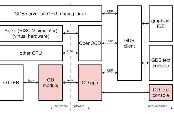
hardware. GDB is a popular and versatile open-source debugger that is designed to work on and with a variety of computer platforms. It is modular and uses well-defined interfaces to connect to other software. Through those interfaces, GDB can be extended to work with a variety of hardware and communicate via a variety of physical connections. While GDB’s core provides a text console user interface, it can also be integrated on the user interface side with graphical IDEs to provide a more rich and convenient user interface. Figure 1 illustrates how GDB interfaces with hardware and user interfaces, with the highlighted blocks representing the deliverables of the project’s current development cycle
Figure 1 - how GDB interfaces with hardware and user interfaces
GDB client to a remote GDB server over a network connection (which may be routed over an actual network or simply within localhost), in which case the two components communicate with each other using the Remote Serial Protocol (RSP). This is illustrated in figure 1 by a GDB server running on Linux. This protocol is also used to connect the GDB client to other
applications that can interface with other hardware that GDB itself doesn’t know how to connect to. One such popular application is OpenOCD, which primarily interfaces with hardware via a physical JTAG connection. OpenOCD is also capable of interfacing with Spike, a RISC-V simulator, via another network connection. In both cases, the GDB client sees OpenOCD as a GDB server providing a standard interface to the hardware (physical or simulated).
The future goal of the OTTER debugger (OD), is for the OD app to similarly interface with the GDB client. Although the current project development cycle won’t provide that interface yet, design decisions were made with that future integration in mind. In the meantime, the OD app will provide its own text console user interface.
Extending OpenOCD directly was considered, but it was decided to develop the OD app independently from OpenOCD. The primary use case of this debugger is for CPE 233 students who use the Basys3 FPGA development board to implement their OTTER. Since the most convenient connection between the PC and the Basys3 board is a standard serial port encapsulated in the USB protocol, the simplest way to interface with the OD module in the OTTER is to design the OD app to use that serial connection directly. Attempting to use JTAG would require both implementing the JTAG protocol in hardware (separate from the JTAG connection that is used to program the FPGA), and using a special cable to connect that JTAG interface (likely through the PMOD port) to an adapter connected to the PC.
Before this OTTER debugger, students had two main options for debugging
would not be able to debug interaction with any custom hardware attached to their OTTER, such as LEDs, switches, or a VGA monitor, and any flaws in their hardware design would be missed. Or they could run their OTTER and RISC-V code in a Verilog simulator, but simulation of custom hardware (especially VGA or keyboard) would be limited and inspection/modification of registers and memory could be cumbersome.
Design
Constraints
The project design was influenced significantly by three primary goals: provide a system that students can use in the early stages of implementing their OTTER, make its integration with their OTTER intuitive, straightforward, and low-level, and build a foundation for future integration with GDB.
There are two main approaches to how debuggers interact with the hardware. On a typical x86 PC, debuggers such as GDB work within an environment that has an operating system. They usually set code breakpoints by replacing an instruction with an invalid opcode to trigger an interrupt. Then they read/write memory and registers by executing standard CPU instructions. In other words, software is used to debug software. The other main approach is to tap into the underlying hardware, and read/write memory and registers via an out-of-band hardware interface, often JTAG.
proven correct. As students implement their OTTER, they start with the core functionality, namely memory, registers, program counter, ALU, and FSM. At this point, they begin debugging their implementation to find mistakes in the ALU, instruction decoder, and other components. If the debugger worked by executing instructions on the OTTER to read/write memory/registers, any flaws in the OTTER would confound the debugging attempt.
So by implementing the debugger with direct low-level taps into the relevant
components, and keeping all debugging control flow in the dedicated already-proven module and app, the debugger is usable earlier on. And the approach is more intuitive for the students, as they see the direct connection between the debugger and the components being
read/written.
The project ultimately aims to build a foundation for future integration with GDB, the popular open-source debugger. GDB is designed in a modular fashion, with any hardware integration (GDB server) separate from the user interface (GDB client), and with a well-defined communication protocol between the two. The next step after this project is to expand the PC-side app to communicate via GDB’s client/server protocol so students can run GDB or a graphical interface on top of it, and have it interface with the OTTER through the PC-side app. Thus, the choices made in this project regarding which functionality it provides (e.g. read one register, change the program counter, set a breakpoint, etc) were made after researching the GDB protocol and the minimum functionality it requires to work on any hardware.
Hardware Taps
At least while the OTTER is paused, it is able to temporarily override anything the OTTER would normally be doing with the non-FSM components. This is done through “taps,” which pass through normal operations when not activated, but give precedence to operations from the debugger when activated.
Note that currently, the OD module will use the taps to process commands even when the OTTER is not paused, though doing so would cause any normal operations to be lost. It expects the OD app to avoid doing so.
The use of these distinct taps keeps the block diagram simple. They minimize the apparent complexity, and help the student focus on the OTTER architecture during the design process. The student can simply ignore the taps when working on the OTTER implementation, as the taps don’t impact normal operation until the debugger activates them, generally during a pause.
See the integration section of this report for diagrams of how the taps affect component operation.
Signal Naming Convention
For consistency, all the taps use the same signal naming convention, even though the original OTTER design uses different names for the same functionality from one component to the next (e.g. the PC’s ld, the RF’s en, and the MEM’s memWrite all perform the same function). The convention, derived from that of many Xilinx modules, is as follows:
● tap_en (debugger to component): activate the tap, suppressing normal operations and allowing the debugger to read or write the register/memory
● tap_addr (debugger to component): if the component stores multiple values, the address/index/ID of the location within the component, otherwise omitted (e.g. PC) ● tap_din (debugger to component): the data to write to the component at the given
address (if applicable), if the tap is activated (en) and we is asserted
● tap_dout (component to debugger): the data read from the component from the given address (if applicable), which is arbitrary if the tap is not activated
Component Operation Injection
Operations are injected through the taps by muxing the relevant input signals based on the taps en signal. When tap_en is asserted, the underlying component gets its write-enable, address, and data-in signals from the debugger through the tap signals, rather than from the normal data/control path. When the tap is enabled, any normal operation is ignored. The tap_dout signal is generally routed directly to the component’s normal output. Thus when the tap is not active, data from other addresses will likely appear on this signal, but the debugger ignores it unless it has activated the tap to intentionally read or write.
There are a couple variations to note however. The OTTER is designed with
OTTER Control Unit FSM
The debugger needs to be able to reset the rest of the OTTER, including the FSM, and pause the FSM between instructions. For the reset, the debugger sits between any external reset signal (e.g. a board button) and the rest of the OTTER. It passes through any external reset, but additionally asserts reset upon request from the OD app.
For pausing, the debugger can assert the cu_pause signal at any time. But the OTTER FSM will only respond to that at appropriate times, namely right before directing a fetch. The OTTER FSM generally cycles through the fetch, execute, and (for memory loads only) write back states. Before proceeding to the next fetch (or if being reset), it first checks if an interrupt is pending, and if so, goes to the interrupt state for one cycle, during which it jumps the PC to the ISR. The FSM doesn’t let the debugger pause the OTTER between an instruction and a jump-to-ISR. This is intended to avoid the situation where the OD app thinks a particular instruction is about to (fetch and) execute, but actually a jump-to-ISR is about to happen first. Instead, pausing is allowed only after any jump-to-ISR. The goal is for all the OTTER’s state during a pause, to always represent the state it will be in during the following fetch (after unpaused). Thus, no changes in other parts of the OTTER (e.g. registers, PC, etc) should change on the FSM’s transition from paused to fetch.
in the paused state, pausable is held low, as this helps the debugger avoid getting stuck when paused on a hardware breakpoint.
Serial Protocol
The OD app and OD module communicate with each other via standard serial. This protocol was chosen because the Basys3 FPGA development boards provide tunneling of a virtual serial port on the PC to RX/TX pins in the FPGA accessible to the logic. By using this, no additional cabling or adapters are needed to operate the debugger. The most common settings were chosen: 1 start bit, 8 data bits, no parity bits, and 1 stop bit. And although the debugger module can be easily configured for an arbitrary speed via a parameter, 115,200 baud was chosen for the default speed. Since each byte takes 10 bits including start and stop, it is possible to transfer data at 11,520 KB/s.
Synchronization
To simplify the protocol and avoid any possible race conditions, it was decided to have the OD app initiate all communication, with the OD module only sending data in response to app commands. Also, all communication is done in 32-bit word chunks, as this OTTER configuration operates on 32-bit values for most things, such as addresses, register contents, and most memory accesses.
However, the serial protocol operates one byte at a time, so if the app or PC
seconds of silence elapse in the middle of a multi-word command or data stream, the module responds with an error and returns to the idle state.
Message Validation
In early testing, data corruption happened sporadically, often related to certain bytes or combinations of bytes sent over the serial port. It was ultimately discovered that there were numerous settings on the PC side, that defaulted to mangling data in various ways, such as translating newlines between Unix and Windows style, treating certain bytes or combinations thereof as control codes, echoing data received, etc. These issues differed on different systems, such as Mac vs Linux vs WSL in Windows.
So to make the protocol more robust, and avoid seemingly random symptoms, a
validation scheme was applied to the OD module/app protocol. All command codes are 3 bytes long with a checksum (a simple XOR of the 3 bytes) as the 4th byte. All commands are echoed back to the app so the app knows the command was successfully received. And all subsequent data transferred, such as command arguments or data in either direction, is also run through a checksum algorithm (a simple XOR of all words). The module sends back the total checksum of all data transferred in either direction, as a single word, at the end of the full exchange for that command. The app verifies that it received the expected echo and correct checksum, and reports a communication failure to the user otherwise.
Commands
● The app sends any command arguments to the module. (args) ● The app sends any data destined for the OTTER. (wdata) ● The module sends any response data to the app. (rdata)
● If the expected number of words were sent and received, and if the command involved more than just the command word and its echo, then the module finalizes the exchange by sending the checksum of all data transferred in either direction since the command echo. (cksum)
The following commands are currently implemented:
● RESET_ON: put the OTTER into the reset state (memory can still be written) ○ no args, no wdata, no rdata
● RESET_OFF: take the OTTER out of the reset state ○ no args, no wdata, no rdata
● WRITE_MEM_RANGE: write multiple words to sequential memory locations starting at the specified address
○ args = {addr, num_words}, wdata = 1+ words, no rdata
● PAUSE: put the OTTER into the paused state (can be combined with reset to pause upon release of reset) after completing the in-process instruction and/or jump-to-ISR
○ no args, no wdata, no rdata
● STEP: proceed to execute the one instruction currently paused at, and return to the paused state (after any pending jump-to-ISR), or just pause if not already
○ no args, no wdata, no rdata
● STATUS: report the pause and reset conditions (any possible combination of these two conditions can occur)
○ no args, no wdata, rdata = {bit1: pause, bit0: reset} ● READ_MEM: read a single word from memory
○ args = {addr}, no wdata, rdata = 1 word ● WRITE_MEM: write a single word to memory
○ args = {addr}, wdata = 1 word, no rdata
● READ_REG: read a single word from a register (PC, RF, or CSR) ○ args = {addr}, no wdata, rdata = 1 word
● WRITE_REG: write a single word to a register (PC, RF, or CSR) ○ args = {addr}, wdata = 1 word, no rdata
● SET_HW_BREAK: set a hardware breakpoint, where execution should pause ○ args = {index}, wdata = {addr}, no rdata
● CLR_HW_BREAK: clear a hardware breakpoint ○ args = {index}, no wdata, no rdata
Hardware Module
Some characteristics of the module are parameterized. Since the serial transceiver needs to operate at a specific speed, but the OD module can’t independently determine the frequency of its clock signal, there is a parameter that the OTTER must use to inform the OD module of its clock speed. This is passed along to the serial transceiver so it can count the appropriate number of clock cycles between bits sent and received over the serial lines.
The baud and timeout parameters determine the timing of serial communication. The baud rate must match between the OD module and the OD app. The timeouts don’t need to match between the module and app, but should be set to high enough values to allow for temporal hiccups in the stream of bytes and words from the PC, while minimizing the chance that a quick restart of the app after a communication glitch will result in misunderstanding between the module and app.
Another parameter is the number of hardware breakpoint registers/comparators to infer. If this is changed, the corresponding macro in the OD app should also be changed to match. The number of breakpoints is a tradeoff between the potential desire for the user (or GDB) to activate many simultaneous breakpoints, and the resource requirements of a register and comparator for each, as well as the gate fanout for connecting one next-PC signal to multiple comparators.
Serial Transceiver
One of the more complex parts of the module is the serial transceiver. Compared to the system clock speed, serial bits are very slow and span a large number of system clock cycles. If a raw physical serial connection is being used (rather than a virtual one through USB where the signal is already cleaned up), the edges of the signals on the serial lines can be noisy. Thus a serial transceiver should attempt to avoid the noise by either oversampling or simply seeking the temporal center of the bits based on the first edge of the start bit.
As sending and receiving serial communication is widespread among hardware designs, it was decided to not implement this from scratch but obtain a polished implementation from another developer. Modules for sending and receiving at the byte level were obtained from nandland.com (see the references section of this report). These modules (uart_rx and uart_tx) signal to their parents when one byte has been completely received or sent. Additional modules to operate at the word level (uart_rx_word and uart_tx_word) were then developed on top of the byte-level transceiver, to notify the OD module only when an entire word has been sent or received.
mid-byte, it will still be able to finish sending or receiving the entire byte and stay in sync with the OD app.
State Machine
The OD module’s state machine sequences responses to and operations in support of commands received from the app. It spends most of its time in the idle state, the only state in which it accepts commands. Once a valid command is received, it begins waiting for arguments, or data as appropriate for the command. If the timeout expires (2 seconds by default) without the module having received the expected words for the command, an error code is sent back to the app, and the FSM returns to the idle state. The FSM also ensures that the serial transmit line is free before initiating transmission of another word. There is no timeout for sending because the serial transceiver simply sends the bits in order without any means of pausing or confirming receipt, thus the FSM won’t hang waiting to send.
The following commands are currently supported. This is the same list of commands as above in the serial protocol section, but detailing how the module implements the commands:
● RESET_ON: sets the mcu_reset persistent signal (stays set until RESET_OFF is received)
○ no args, no wdata, no rdata
● RESET_OFF: clears the mcu_reset persistent signal (stays cleared until RESET_ON is received)
○ no args, no wdata, no rdata
○ args = {addr, num_words}, wdata = 1+ words, no rdata
● PAUSE: sets the cu_pause persistent signal (stays set until STEP or CONTINUE is received) and waits for the FSM to enter the paused state before echoing the command
○ no args, no wdata, no rdata
● STEP: briefly clears cu_pause (for one clock cycle), sets it again (stays set until STEP or CONTINUE is received), and waits for the FSM to reenter the paused state before echoing the command
○ no args, no wdata, no rdata
● CONTINUE: clears the cu_pause persistent signal (stays cleared until PAUSE is received or a hardware breakpoint is hit)
○ no args, no wdata, no rdata
● STATUS: reports the state of the mcu_reset and cu_pause persistent signals to the app
○ no args, no wdata, rdata = {bit1: pause, bit0: reset}
● READ_MEM: activates the memory tap to read a single word from the specified address in memory, waits one cycle for the data to arrive from memory, and sends it to the app
○ args = {addr}, no wdata, rdata = 1 word
● WRITE_MEM: receives a single word from the app and activates the memory tap to write it to the specified address in memory
○ args = {addr}, wdata = 1 word, no rdata
○ args = {addr}, no wdata, rdata = 1 word
● WRITE_REG: receives a single word from the app and writes it to the specified register (address determines PC, RF, or CSR)
○ args = {addr}, wdata = 1 word, no rdata
● SET_HW_BREAK: sets the specified (by index) hardware breakpoint to the given address and activates it, which triggers a pause if and when the program counter changes to the address
○ args = {index}, wdata = {addr}, no rdata
● CLR_HW_BREAK: deactivates the specified (by index) hardware breakpoint ○ args = {index}, no wdata, no rdata
Register Numbers
The OTTER debugger considers the program counter (PC), general purpose registers (RF), and control/status registers to all be just registers in a broad sense, with unique numbers to distinguish them. This mimics the behavior of Spike when attached through OpenOCD to GDB. The module routes tap activations and operation details to the appropriate component’s tap based on the register number. The register numbers are translated as follows:
● 0-31: RF ● 32: PC
● 65-4160: CSR (register number = CSR # + 65) ● others: undefined behavior
● mstatus: CSR 0x300 (768), OD register number 833 ● mie: CSR 0x304 (772), OD register number 837 ● mtvec: CSR 0x305 (773), OD register number 838 ● mepc: CSR 0x341 (833), OD register number 898
PC Application
The OD app bridges the gap between the user (or GDB client in the future) and the hardware. It communicates with the OD module using the serial protocol, programs the OTTER on startup, and optionally enters an interactive debug mode where the user can use all the commands that the OD module supports (see the user interface section of this report).
Raw Serial Configuration
The app needs unfiltered unmodified access to the serial port, as communication with the OD module uses a binary protocol with no regard for the nuances of newlines in various operating systems or cursor/formatting control codes. It was a bit of a challenge determining all of the necessary flags for configuring the Linux serial driver (through the tcsetattr library call) to simply pass all bytes along unmodified. By default, the driver does special stuff when certain control codes are sent over the line. It also sometimes echoes data received, and/or translates newlines between Unix and Windows style.
the University of Minnesota was invaluable in tracking down some of the remaining configuration flags.
In case the app is being used on a system on which other serial apps expect all the default behavior, the app saves all the serial configuration on startup, and registers a Ctrl-C signal handler and an exit handler so it gets a chance to restore the serial configuration before the app exits.
Modularity
The app is written with many small functions, building up from simply sending or receiving a word, to waiting for timeouts and expecting certain responses, to handing all communication for a specific OD command. This will make future development easier, when higher-level functions are written to translate GDB commands to sequences of OD commands.
At the lowest level, the send_word and recv_word functions ensure that an entire word is sent or received, handling error cases, incomplete transmission, and user interrupts (Ctrl-C). They rely on the serial configuration at app startup for specifying how much time is allowed between bytes and how many bytes it waits for. The termios article from unixwiz.net was helpful in understanding how timeouts vs minimum bytes can be balanced.
The wait_readable function deals with any timeouts between the words of a command exchange. This allows for a longer time between words than between bytes. The OD
module-app protocol always transfers whole words at a time, but there could theoretically be small delays between words for certain commands that wait for some action to occur or complete before proceeding.
correct, such as the correct checksum or matching command echo. The expect_any_word function simply encapsulates the timeout handling, while not restricting the response to a particular word, and the expect_timeout function could be useful in the future if needed to ensure the line is idle at startup or after a command.
Checksums are used on all communication, so there is a macro (APPLY_CMD_CKSUM) for applying the checksum to command codes, and a function (verify_checksum) for verifying that the correct checksum is received from the module at the end of a command exchange. A global variable is used to accumulate the checksum on all data sent or received after the command echo.
For long-running commands such as WRITE_MEM_RANGE which is used for
programming the OTTER (writing a program binary to instruction memory) at app startup or on request, the function flush_and_show_progress is used to provide feedback to the user on the completion percentage.
Built upon that foundation, there are functions for each of the OD commands as follows: ● RESET_ON: enter_reset_state
● RESET_OFF: exit_reset_state
● WRITE_MEM_RANGE: write_mem_range, which is factored into a few other unmentioned functions
● PAUSE: set_paused_status ● STEP: single_step
● CONTINUE: clear_paused_status ● STATUS: get_status
● READ_REG: read_reg ● WRITE_REG: write_reg
● SET_HW_BREAK: set_hw_breakpoint ● CLR_HW_BREAK: clear_hw_breakpoint
User Interface
In lieu of future GDB integration, a barebones user interface is provided by the OD app. It simply enables the user to issue all of the above-mentioned commands through their
respective functions. The app always programs the OTTER on startup by using
write_mem_range to send the contents of a binary file, after putting the OTTER into reset with enter_reset_state. Then if the user opts for debug mode, it pauses the OTTER
(set_paused_status) before releasing the reset (exit_reset_state) so execution pauses at the written program’s first instruction. If not using debug mode, the OTTER is released from reset without pausing, useful for simply running a program on the OTTER that was compiled on the PC.
Command Line Arguments
When running the OD app, the user must specify a binary file to program the OTTER with, as the first command-line argument.
The user must also specify the serial port to use as the second argument. On Linux, virtual serial ports routed over USB (as is the case for the Basys3 board), are usually named like “/dev/ttyS1” where the number 1 may differ. No auto-select feature is offered, but the OD
should keep in mind that the Basys3 provides two virtual serial ports, one for configuring the FPGA (used by Vivado to write a bitstream) and the other for communicating with logic in the FPGA (the OTTER).
If the word “DEBUG” (all caps) is given as the third argument, the interactive debug mode is entered. Otherwise, the app exits after simply programming the OTTER.
Commands
Once in interactive debug mode, the app uses the readline library to provide a featureful command prompt, including history accessible by the up and down keys and filename
completion with the tab key. Developers need to have the libreadline-dev (for Ubuntu, might differ for other distros) package installed when compiling the OD app.
Commands can be given by their full name or by their first 1 or 2 letters as detailed below. Arguments (if any) are separated by spaces. Numbers can be provided in hex (0x prefix), octal (0 prefix), or decimal (no prefix). The list of commands and their usage, as well as some notes, can be obtained by entering “help” or “h” at the prompt. Enter “quit” or “q” to exit the app.
● RESET_ON: reset or r ● RESET_OFF: unreset or u
● WRITE_MEM_RANGE: wfile or wf ● PAUSE: pause or p
● STEP: step or s
● READ_REG: rreg or rr ● WRITE_REG: wreg or wr ● SET_HW_BREAK: bset or bs ● CLR_HW_BREAK: bclear or bc
It is important to remember that because the OD module can only send data to the app in direct response to a command from the app, the app will not receive a notification when a breakpoint is hit. The user currently must periodically check the OTTER’s status with the status command. In the future, this could be improved by having the app poll the module in the
background, so the app can remain responsive for an on-demand pause command while also notifying the user if the OTTER pauses at a breakpoint.
Integration
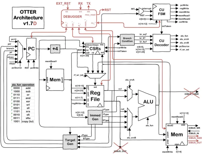
Figure 2 - high-level block diagram
(credit to Joseph Callenes for original diagram in black)
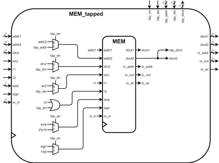
Before adding the wrapper around the memory module, route the IO address and data output signals through the memory module so that the debugger can access external
memory-mapped devices through the memory system. This can be accomplished by adding IOBUS_ADDR and IOBUS_OUT outputs to the memory module, assigned to the addr2 and din2 inputs respectively within the memory module. Then adjust the routing in the main module accordingly.
To connect the debugger to the PC-side app via standard serial, add a RX input and a TX output to the OTTER’s main module, and route them to the debugger. Also route them through the external top-level module appropriately and update the constraints to connect them to the RS-232 signals on the Basys3.
The signals shown in figure 2 that have arrowheads at both ends represent groups of signals, some in one direction and some in the other. Signals should be created in the OTTER’s main module to link the ports on the debugger to the appropriate components, for example linking rf_addr and rf_dout on the debugger module to tap_addr and tap_dout respectively on the RF module’s wrapper (see next section), and linking cu_pause and cu_paused on the debugger module to pause and paused respectively on the CU FSM module.
Component Wrappers
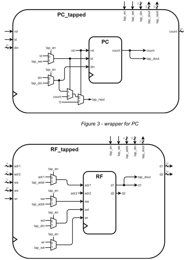
Figure 3 - wrapper for PC
Figure 6 - wrapper for MEM
State Machine Modifications
applies to any other action taken between instructions, such as writing to a register. While paused, the debugger expects that all registers (including CSR and PC) and memory are as they will be during the following fetch.
Figure 7 - modified state diagram
This form of state diagram, with intermediary points between states, may be unfamiliar to students. Those points (the small solid black circles) are not states. They are just a more
And if that transition is to occur on the next clock edge, the pausable signal (a Mealy output) should be asserted. Similarly, there is a transition from WB to INTER that occurs if int is true, regardless of load or pause, and in such a case, pausable should not be asserted.
Note that load is a shortcut for the current instruction opcode being a load instruction, in which case, the writeback (WB) is needed to finish the instruction before proceeding. The pausable signal, which is routed to the debugger, should only be asserted when the FSM would consider the pause signal, which is only right before a fetch (unless about to pause). The interruptible signal is not routed outside the FSM, but may be helpful internally. Note that interrupt-jumps take precedence over pausing, to avoid the debugger thinking an instruction is about to fetch and execute while actually a jump to the ISR would occur first.
Demonstration
Figures 8-17 show operation of the OD app connected to the reference OTTER
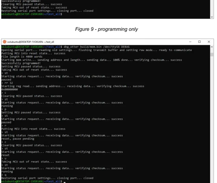
integration, running in Ubuntu within WSL1 on Windows 10. Figure 8 shows the usage page. In figure 9, the OTTER is simply programmed with the test_all program, after which the program is running on the board as normal. The board switches 2, 1 and 0 are set to up, up, and down respectively, so the tests run at human-readable speed and any errors will cause the test suite to pause with an error code. In figure 10, the OTTER is programmed again but this time debug mode is entered, and the OTTER is initially placed in the pause state at the first instruction before prompting for commands. The various combinations of pause and reset are then demonstrated.
the memory tap would cause normal memory operations to be ignored briefly. In figure 12, various registers are read, written, and reread, namely t0 (OD register 5), the program counter (OD register 32), and mtvec (OD register 838). Register access is not permitted when the OTTER is running normally, for the same reason as for memory access. Note that some registers are unwritable (e.g. mtvec) while the OTTER is in reset; writes in such a case simply fail silently because the hardware reset overrides those writes to keep the registers in a desired initial state.
The app keeps a cached copy of the OTTER’s status, updating it when status-changing commands complete. However keep in mind that the app currently doesn’t know if a breakpoint is hit, so it may think the OTTER is running when it’s actually paused, hence the suggestion for the user to request a status check. Unfortunately, if the OTTER were reset by an external signal (e.g. a board button), the app would not be aware if it was now running while the app’s last knowledge was that it was paused. Future development of the app could add a status check before every command, at the expense of more serial traffic.
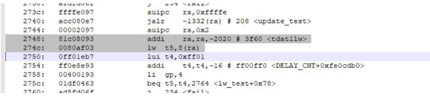
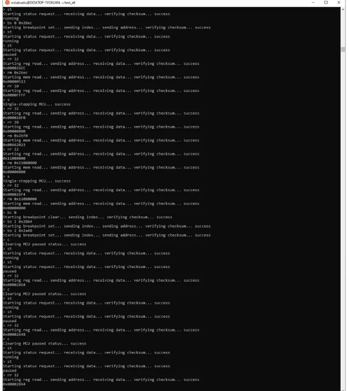
Figure 14 demonstrates a simple debugging session over a couple lines of the test_all program highlighted in figure 13 (from an independent text editor viewing the program.dump for test_all). At each instance in the screenshot where the status (st) command was run twice in a row, there was a gap of time between, during which the lights on the board were watched until they stopped changing. The second status command confirmed that execution had actually paused. After each time the OTTER paused, the program counter was read (register 32), and when relevant, the next machine instruction was read from memory at the corresponding address.
pauses at that instruction address, the value in ra (register 1) is checked, the OTTER is single-stepped through the addi, and ra is checked again to confirm that it changed to the desired value. Before executing the following lw instruction, t5 (register 30) and the memory that the lw will target are read. After single-stepping through the lw, t5 is read again to confirm that it changed to the value in memory. Then the first breakpoint is cleared and two others are set for other points in test_all. Since test_all loops through all tests repeatedly, it is expected that the two new breakpoints will be hit repeatedly in alternating order. Continuing the OTTER a few times confirms that the first breakpoint is no longer active and the two new ones are hit as expected. When GDB integration is complete, this process will be simpler and the appropriate lines of the test_all code will be displayed automatically in GDB as execution is paused or breakpoints are hit.
Figure 8 - usage page
Figure 9 - programming only
Figure 11 - reading and writing memory
Figure 15 - before reading and writing devices
Figure 16 - reading and writing devices
Completed Deliverables
● OD module and app:
https://github.com/KeefeJ/otter_debugger
● Integration instructions:
See the integration section above, and review the design section as needed. ● Reference integration/implementation:
Cal Poly instructors can email Keefe at [email protected] for access.
Future Work
GDB Integration
It is expected that one command from the GDB client will result in the OD app issuing multiple commands in sequence to the OD module, as the OD module implements just the fundamental building blocks that GDB relies on. For example, GDB’s “g” command, which reads all general registers, will likely translate to 33 individual READ_REG commands to the OD module, the 32 general registers and the program counter (register 33).
OD app will also likely need to respond to GDB client’s request for processor
information, with an XML-formatted list of general and special (CSR) registers. This would not necessarily involve any communication with OD module, unless the project is expanded to support multiple variations of RISC-V, such as the floating-point extension or 64-bit
configuration, in which case it may be desirable to query OD module for its build info.
There is one design aspect that will be a bit tricky to build upon: that OD module never initiates communication but always only responds to the OD app. When GDB sends the continue command, it expects no response until the hardware pauses again (i.e. due to a breakpoint). However, the OD module will respond right away confirming that execution has continued, and will not inform the OD app when it pauses. The OD app will need to poll the OD module with the status command, and only reply to GDB when the status indicated paused.
Adapting to Pipelined OTTER
memory) will not always cleanly represent the state between two instructions from the ISA perspective.
Also, the current state of the program counter would be multiple cycles out of sync with the state of registers and memory from the ISA perspective. Although it could report the
program counter as previously recorded and passed along the pipeline stages to the final stage, the memory vs registers out-of-sync issue is harder to work around.
One approach may be to simply pause the fetch stage and let the pipeline empty out, whenever the debugger requests a pause. This has the benefit of ensuring everything is at a consistent state from the ISA perspective, as if each instruction had been executed one at a time. However, this introduces the chance of exposing mistakes in the student’s implementation of pipeline stalls/squashes, especially if they only designed it for the specific combinations of instructions that could occur without a debugger.
In addition, in CPE 333, the OTTER’s memory system is extended to handle caching, requiring the architecture to handle memory operations taking a variable number of clock cycles. A signaling protocol has been developed to handle such variable-latency memory (VLM)
operations, and adapting the debugger to that protocol for the memory module shouldn’t be very difficult. The debugger’s FSM currently assumes that a memory operation will always complete the cycle after initiation, but the feedback from the VLM protocol could be easily used to hold the debugger’s FSM in a waiting state until the operation is complete.
References
http://openocd.org/documentation/
https://riscv.org/software-tools/riscv-gdb/
https://riscv.org/specifications/debug-specification/
https://www.youtube.com/watch?v=_mRLFrdzSN4
https://github.com/riscv/riscv-isa-sim#debugging-with-gdb
https://www.embecosm.com/appnotes/ean4/embecosm-howto-rsp-server-ean4-issue-2.html
https://sourceware.org/gdb/current/onlinedocs/gdb/Remote-Protocol.html
https://sourceware.org/gdb/onlinedocs/gdb/Remote-Stub.html
https://www.gnu.org/software/libc/manual/html_node/Noncanon-Example.html
https://www.cmrr.umn.edu/~strupp/serial.html
http://unixwiz.net/techtips/termios-vmin-vtime.html
https://www.nandland.com/vhdl/modules/module-uart-serial-port-rs232.html
https://ibex-core.readthedocs.io/en/latest/cs_registers.html
https://sourceware.org/gdb/wiki/GDB%20Front%20Ends
https://github.com/riscv/riscv-isa-sim/blob/master/README.md