Receiver for QAM Modulation
Amit Kumar Dutta
Calcutta Institute of Technology, WB, India
ABSTRACT
In Internet data transmission, the throughput of 45 Mbps is achieved. Now the goal is to increase the data rate further to 100 Mbps and beyond. We designed a Frequency Division Multiple Access system for that and realized it using Q-Dot technology. The principal reason for coherent demodulation in LAN is the size of PLL in Q-Dot circuit. It also allows higher capacity than ½ achieved so far.
1.0 INTRODUCTION
High speed data communication is evolving according to advancement in device technology. Recent demand in research is for data transmission nearing 100 Mb/s rate in LAN, TV cable and fiber optics communication. In this article we find Wideband Frequency Division Multiple Access (WFDMA) as the solution to the problem along with a QAM modulation scheme. In absence of fading this is sufficient to meet the goal of a 100 million bits/second. Recently there is advancement in WCDMA over capacity. This will be possible to achieve if we can implement linear phase analog filter. To achieve higher capacity in WCDMA we need to implement m sequence as the PN sequence and delay locked loop in the receiver. Otherwise the same capacity increase will be possible in differential FDMA transmission (PAM/PSK) with lesser burden on the filter. Moreover FDMA receiver will consume much less power.
The organization of the paper is as follows. Section II introduces the topology for higher capacity. Section III and Section IV introduce the Costa’s feed forward circuit to extract carrier for PAM and QAM. In Section V we discuss about the phase locked loop modified structure to recover carrier and data clock. Section VI is about the circuit detail in Q-dot technology. Section VII is about a high speed demodulator. Section VIII is about super heterodyne receiver and we conclude the paper in the next Section.
2.0 ON TOPOLOGY FOR HIGHER CAPACITY
Recently it is found that design of receiver becomes possible in case the consecutive frequency bands are not used. This achieves ¼ capacity. This capacity problem is addressed here. In case the transmission is using a LC oscillator, in magnetic field it will be a sinusoidal oscillation. Then the capacity can be doubled that is the capacity is ½ because of I and Q modulation. If we use a capacitor as an integrator and no sample and hold circuit, we can use all frequency bands at our will neglecting the guard band then we achieve a capacity of 1. The phase locked loop uses a VCO whose output is modulated twice the data rate. The capacity can be further improved using multi level PAM. Then the last improvement comes from the use of QAM modulation to 2.
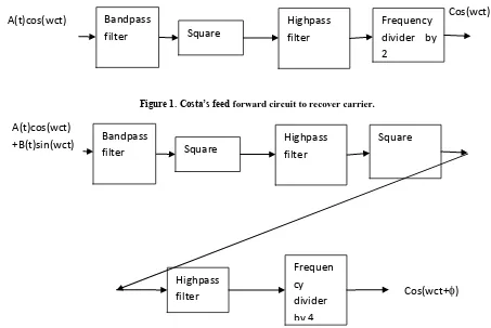
3.0 CLOCK RECOVERY FOR PAM- COSTA’S LOOP
This is a feed forward circuit as explained in Figure 1. We pass the incoming signal through a band pass filter to get rid of the interference from adjacent channels. The PAM signal is given by A(t)cos(wct) where A(t) is the data and cos(wct) is the carrier. Then we square it and get rid of dc component by passing it through a high pass filter. This results into a double of the wc frequency and we get wc term by frequency divider. Thus we get cos(wct+) where is the phase delay associated with generated signal.
4.0 CLOCK RECOVERY FOR QAM- COSTA’S LOOP
The Costa’s feedforward circuits have the generation of higher frequency and that causes EM radiation. Moreover we need a bandpass filter which is difficult to design.
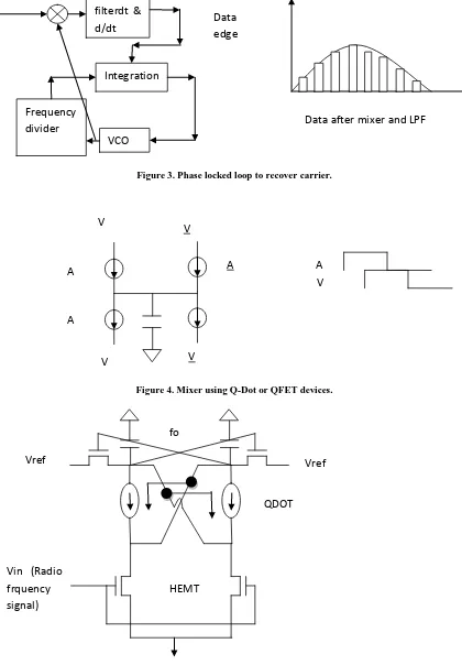
5.0 PHASE LOCKED LOOP FOR PAM & QAM
Costa’s feedforward circuit is simple but requires superheterodyne structure to reduce the higher frequency component. This forces us to look for phase locked loop structure. Unfortunately, the signal A(t)cos(wct) cannot be used to lock on wc frequency, as the error signal (the mixer output) is data dependent. This causes it to be converging or diverging even if we lock to wc by making A(t)=1 at the synchronization time. This made digital transmission almost impossible at high rate and higher frequency.
This is circumvented by finding the data edges of the mixer output and setting a frequency divider of VCO output. The VCO output has the same frequency as wc and the data clock phase locks to the data edges. This makes the PLL to phase synchronize and derive the carrier frequency at the same time. Now the range at which PLL will converge will be decided by the signal at the mixer that is A(t)sin(w-wc)t term after low pass filter. If w-wc is lower in compare to A(t) signal rate, then data edge could be found. For QAM signal, the A(t) is kept equal to B(t) during synchronization time. This method of clock recovery for PAM or QAM is most suitable for LAN or TV Cable. This is shown in Figure 3.
6.0 CIRCUIT ELEMENTS
The Q-Dot analog PLL circuits will be a reality which could be found in reference [5] or variations of that. We know that Q-Dot oscillator works at very high frequency which means if controlled properly we can realize very high frequency Voltage Controlled Oscillator (VCO) and mixer for local oscillator. At first we look at the high frequency CMOS mixer circuit as we find it in reference [3] which is a Gilbert cell or a voltage switching mixer. We find the Q-Dot mixer circuit as proposed in Figure 4, is a variation of voltage switching mixer. The mixer circuit could be explained as shown in Figure 4, considering a bipolar signal to be demodulated using a bipolar clock signal. If we multiply we get the signal as +,-,-,+ and if frequency matches the integration of the area will be zero. The mixer has four branches, each injecting charge or taking charge out of a filter depending on polarity and magnitude of two signals. The mixer is of two kinds, one using Q-Dot devices for 2 level PAM, the other using QFET devices for multilevel PAM. The QFET devices work in linear region for multilevel PAM.
The VCO is a current steered oscillator with switched dc voltage as can be found in [3]. The circuit is a modified version of the Q-Dot VCO first reported in reference [5]. Here we bias the circuit by switching the Vref dc voltage to the oscillating two nodes. When one node is high, the other node is switched to the Vref dc voltage and vice versa. The VCO is shown in figure 5. The filter is a RC filter whose time constants are decided by the speed of the sample and hold circuit. The switch is implemented by HEMT device for high speed or by NMOS for low speed. The resistance value and the capacitance value of sampler is very critical as it should be accurate as well as fast and integrator in behavior.
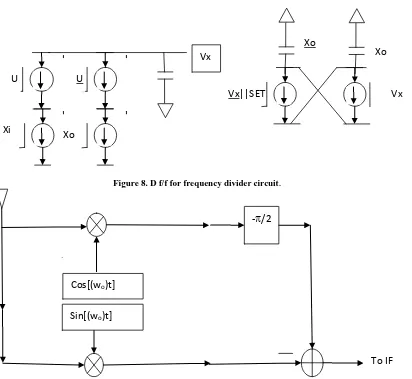
We need a frequency divider circuit and we choose the divide-by-2 circuit using D flip/flop. The D flip/flop is clocked by VCO output and the Q_bar is connected to the Data_in. The Q is connected to the CLOCK of next D flip/flop. Now the D flip/flop is set by the edge of the data and the set signal could the repetitive or missing some pulses sometime. We have to generate same clock period as the data period and continuously repeat it. It gets set repetitively and when synchronized the VCO output frequency will be in phase and same as carrier frequency.
7.0 DEMODULATOR CIRCUIT
The demodulator circuit is similar to PLL, except there is no loop here. The signal is taken from the mixer output. This is integrated, compared and latched at the data clock. Because of integration, adjacent channel interference will be attenuated. Hence noise and correlated noise is integrated. We assume that the differential signaling is done at the transmitter. The Figure 6 shows the demodulator, which is true for two levels PAM. It has two mixers for I and Q branches. After multiplication they are low pass filtered. They will be
X* cos(wct+)=1/2[Acos - B sin and
If the carrier is wavering slowly, then there will be a sinusoidal term in the output which we cannot get rid of as A(t) or B(t) is of very high frequency. We find the wavering signal by Costa’s method and vary the Vref accordingly in the comparator of the detector or do a matrix inversion in analog as shown in Figure 10.
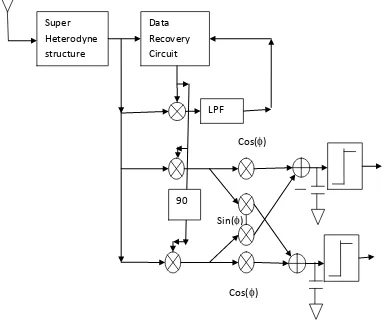
8.0 SUPER HETERODYNE RECEIVER
We can have a super heterodyne receiver instead of using direct down conversion receiver. The RF front end will be as shown in Figure 9. We do not need any band pass filter. The receiver is shown in Figure 10. We use the same principle to get rid of the frequency variation around a stable operating point of DPLL like it Direct Down Conversion. We put the integrator at the end which works both as LPF and as integrator.
9.0 CONCLUSION
A design principle for high speed data transmission is presented here. If we use 25 MHz channel bandwidth, we may transmit 100 Mbps, which could be a possibility provided the circuits mentioned here work. We here mentioned a clock recovery circuit for QAM for level 4, which doubles the capacity from existing one.
REFERENCES
[1]. R. Hanson, L P Kouwenhoven, J R Petta et al, “Spins in few-electron Quantum Dots,” Physics Review [2]. R. Gregorian and G. C. Temes, “Analog MOS integrated Circuits for signal processing,” Wiely series on
Filter
[3]. P. R. Gray and R. G. Meyer, ”Analysis and Design of Analog Integrated Circuit,” John Wiley and Sons, Inc., 3rd Edition
[4]. A.S. Sedra, K.C. Smith, “Microelectronic Circuits”
[5]. A.K. Dutta, “UHF RF Transmitter and Receiver,” IJERSTE ISSN 2319-7463 Vol. 3 Issue 11, November 2014
Figure 1. Costa’s feed forward circuit to recover carrier.
Figure 2. Costa’s feed forward circuit to recover carrier.
Square Highpass filter Square
Bandpass filter
Highpass filter
Frequen cy divider by 4 A(t)cos(wct)
+B(t)sin(wct)
Cos(wct+) Cos(wct)
Square Highpass filter Frequency divider by
2 Bandpass
Figure 3. Phase locked loop to recover carrier.
Figure 4. Mixer using Q-Dot or QFET devices.
Figure 5. Voltage Controlled Oscillator. The Vref is connected by Q-dot / QFET switching devices.
Vin (Radio frquency signal)
HEMT
QDOT fo
Vref Vref
V V
V V
A
A
A A
V VCO
Frequency divider
Integration Lowpass filterdt &
d/dt Data edge
Signal
Figure 6. Demodulator for 2 level QAM in I/Q branch. Carrier and data latch clock come from PLL.
Figure 7. Frequency Divider by 4. We have to introduce a set.
Figure 8. D f/f for frequency divider circuit.
Figure 9. Super heterodyne structure to get rid of RF band pass filter, -/2
Cos[(wo)t]
To IF Sin[(wo)t]
Vx||SET I
d
L
U
I
d
L
U
I
d
L Xi
n g
Vx
I
d
L
Xo og
Xo
I
d
I
d
Xo
Vx Q
D Q
Q D Q CLK
CLK/4 Comparator & SR Latch
Figure 10. Super heterodyne receiver. Sin()
Super Heterodyne structure
Data Recovery Circuit
LPF
90
Cos()