Sunil Jadhav
et al
, International Journal of Computer Science and Mobile Applications,
Vol.3 Issue. 6, June- 2015, pg. 12-20
ISSN: 2321-8363
©2015, IJCSMA All Rights Reserved, www.ijcsma.com 12
ADIABATIC LOGIC FOR LOW POWER DIGITAL DESIGN
Mr. Sunil Jadhav
1, Prof. Sachin Borse
21Student (M.E. Digital Signal Processing),Late G. N. Sapkal College of Engineering,
Nashik,[email protected]
2 Professor in Electronics and Telecommunication Department,Late G. N. Sapkal College of Engineering, Nashik, [email protected]
Abstract
There are so many strategies implemented to reduce the power consumption in CMOS digital design. Many of them are based on complement form and clock signals. In CMOS digital design power consumption can be reduced by reducing the supply voltage, decreasing capacitance and reducing the switching activities. These techniques are not suitable in today’s CMOS design scenario. So many researchers are working on new design techniques which will help in reducing the dynamic power consumption. Most of the research is focused on Adiabatic logic which is proved to be the excellent technique to design the low power digital circuits. In this paper we focus on the adiabatic logic with complementary energy path dual pass transistor logic (DPL-CEPAL). Conventional NAND, NOR and EX-OR/NOR gates are compared with the DPL-CEPAL NAND, NOR and EX-OR/NOR gates. It is proved that DPL-CEPAL technique is superior to conventional technology as far as power consumption is concerned. This DPL-CEPAL technology can be used to design the full adder cell and multiplier cell which are the core part of any ALU processor.
Keywords: Adiabatic logic, Dual pass transistors, Power delay product (PDP), DPL-CEPAL NAND, NOR, EX-OR/NOR, power clock source.
1. Introduction
Recently, the requirement for low power CMOS design has been steadily increasing. More and more research work is concentrated on low power solutions. Moore’s law states that component density and performance of VLSI circuits doubles every year. Energy consumption and performance are the key criteria considered while designing VLSI circuits. The key components of digital computing are multipliers and arithmetic logic unit (ALU). Full adder is basic unit which determines functionality of ALU and multiplier. Micron technology is very advanced now days, which solved the issue of area requirements of computational design. Dimensions of the MOSFETs can be shrunk into sub-micron region as reported in [1].
Adiabatic logic is very good alternative to conventions CMOS designs to realize the low power design. Adiabatic logic configurations minimize the energy consumption to a great extent. The charges stored in circuit capacitors are recycled efficiently. Thus it avoids the energy dissipation as heat. Conventional designs use constant DC source to charge the capacitances whereas adiabatic logic families use time varying voltage supply as power source.
The following mathematical formula shows the lower limit on dynamic power consumption by CMOS design.
(1)
Sunil Jadhav
et al
, International Journal of Computer Science and Mobile Applications,
Vol.3 Issue. 6, June- 2015, pg. 12-20
ISSN: 2321-8363
©2015, IJCSMA All Rights Reserved, www.ijcsma.com 13
This paper describes the same single power clock technique to improve the performance. To reduce the energy consumption dual pass transistor configuration with adiabatic logic is used.
2. Aim and Objectives
2.1 Aim
Our aim is to design low power DPL-CEPAL NAND, NOR and EX-OR/NOR logic which will be the key components of CMOS digital design.
2.2 Objectives
We have proposed new DPL-CEPAL design for NAND, NOR and EX-OR/NOR logic. Asynchronous clocking combined with adiabatic logic is used. We have tested the proposed design for different input frequencies and pulsed power clock frequencies. These designs are faster and excellent in reducing the power consumption.
NAND-NOR are the universal gates and are used to design complex digital circuits. XOR-XNOR is useful in larger circuits design such as full adder and parity checker. Optimised design using DPL-CEPAL is proposed and it is proved as beneficial as far as performance of the larger circuits is concerned.
3. Adiabatic Logic Design
Adiabatic is a Greek term and it is related with Thermodynamics. In adiabatic system transition occurs without energy (in form of heat) lost or gains from the system. In our design we used adiabatic logic to reduce the energy consumption. This differs from CMOS switching which dissipates energy during switching. Considering this technology it is clear that energy is reproduced and reused to perform further calculations. To reduce the dynamic power some approaches are to decrease the physical capacitances and to reduce the switching activity. These techniques are not suitable for today’s power requirement. Most of the work is being done on adiabatic logic design which is very beneficial for low power applications.
Adiabatic logic reduces the switching activities and it reduces the energy consumption. The basic concept is to give stored energy back to power source. Thus it is a simple reversible logic.
Following are the design rules for the adiabatic circuit design.
1. Never turn on a transistor if there is voltage across it. (VDS>0). 2. Never turn on a transistor if there is current flowing through it(IDS≠0). 3. Never pass current through a diode.
These are the conditions regarding the input in all the phases of power clock. Energy is stored in the recovery phase.
3.1 Limitations of Adiabatic logic
1. Circuit has to be implemented with time varying power source which is complex procedure. 2. Operating speed can be slower and my require more area than conventional CMOS.
3.2 Asynchronous adiabatic logic
It is a unique combination of energy saving benefits of adiabatic logic and asynchronous circuits. Asynchronous circuits have built-in sensitivity to variations in power supply voltage. Another advantage of this, in idle state it will not utilize clock signals whereas in synchronous circuits clock signal is given continuously to the entire system and thus it consumes energy and convert it into the heat.
The main advantage of this circuit is lower power consumption and no transistor ever changes the state unless it’s performing a useful computation.
4. Methodology Adopted
Dual pass transistors logic is useful to improve the circuit performance at reduced voltage level. For low voltage, low power and for small power delay dual pass logic is beneficial.[5][7] Pass transistor structure makes it easy to pull the sizing of transistors to get the desired charging and discharging time. Thus the slope of output signal minimizes the power.
Sunil Jadhav
et al
, International Journal of Computer Science and Mobile Applications,
Vol.3 Issue. 6, June- 2015, pg. 12-20
ISSN: 2321-8363
©2015, IJCSMA All Rights Reserved, www.ijcsma.com 14
reduced supply voltages are avoided. This is achieved by adding PMOS transistor in parallel with NMOS transistor.
In CMOS design the important part is to design the power clock because the complete transistor logic shares the same power clock and hence the power clock switching circuit dissipates the most of the power. In synchronous clocking the single clock is shared by large number of logical gates in parallel and hence the switching loss of power clock is more in synchronous clocked circuits.
In asynchronous clocking the energy is locally stored in and stored energy is fed back to power clock source and used for subsequent gates. This technique will help to save the power consumption. This approach is helpful while implementing the adiabatic logic in real time.
DPL-CEPAL (Dual pass logic-complementary energy path adiabatic logic) is efficiently implemented. DPL-CEPAL logic is composed of two PMOS switches to provide the complementary path to the stored energy. Through these switches the stored energy will be fed back to the power clock source. Dual pass logic is situated between clocked power source and constant DC source. The current flowing through the dual pass transistors will depend on the potential difference between clocked power source and constant DC source.
Above explained techniques are discussed in more details in the following sections. Proposed full adder cell is combination of logic part consisting DPL and CEPAL part to provide complementary energy path to reduce the energy consumption.
5. Proposed DPL-CEPAL logic
Our objective is to design and implement energy efficient logic cells using DPL-CEPAL. In DPL-CEPAL two power sources are used one at top which is pulsed power clock and one at bottom which is constant DC or sometimes ground. Two PMOS switches are used to provide the complementary energy path at the top.
In DPL-CEPAL, output logic level is always slightly lower than input logic levels due to the non-adiabatic losses. The main concept is to carry the input signal to the output according to the digital logic.
Generally Complementary power clock is used in complementary energy path adiabatic logic. We have used pulsed power VDD source along with constant DC source.
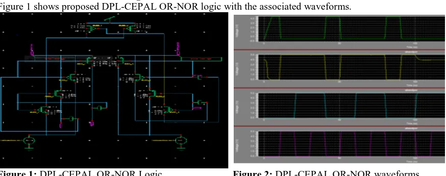
5.1 DPL-CEPAL OR-NOR Logic
Figure 1 shows proposed DPL-CEPAL OR-NOR logic with the associated waveforms.
Figure 1: DPL-CEPAL OR-NOR Logic Figure 2: DPL-CEPAL OR-NOR waveforms
Figure 2 shows the associated waveforms of DPL-CEPAL logic. VDD source is pulsed power clock and constant DC source is connected as shown. Two PMOS and two NMOS are connected as shown to form dual pass logic.
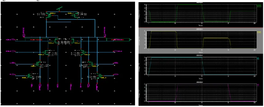
5.2 DPL-CEPAL AND-NAND Logic
Sunil Jadhav
et al
, International Journal of Computer Science and Mobile Applications,
Vol.3 Issue. 6, June- 2015, pg. 12-20
ISSN: 2321-8363
©2015, IJCSMA All Rights Reserved, www.ijcsma.com 15
Figure 3: DPL-CEPAL AND-NAND Logic Figure 4: DPL-CEPAL AND-NAND waveforms
Due to pulsed VDD source there is some propagation delay which will be measured to calculate the power delay product/energy.
5.3 DPL-CEPAL XOR-XNOR Logic
In the same way DPL-CEPAL XOR-XNOR logic is developed and shown with the associated waveforms in Figure. 5 and Figure. 6.
Figure 5: DEP-CEPAL XOR-XNOR Logic Figure 6: DPL-CEPAL XOR-XNOR waveforms
6. Results and Outcomes
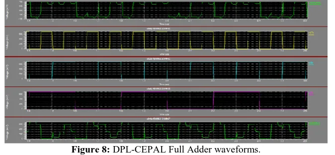
Using the above designed logics a simple full adder cell is designed as shown in Figure. 7 with associated waveforms.
All the schematics are done in Tanner EDA tool using 180 nm technologies. The pulsed VDD and DC source is 0.7V.
The results and outcomes section show the various reading taken to analyze the performance of the proposed design. As per the advancement in VLSI low power technology up to the year 2013 we can use 0.7V as VDD for MOS transistors with threshold voltage VT 0.3V. This helps reducing the power consumption. The lower nm technologies like 45nm can be used but if we go for lower dimensions technologies we have to use the higher VDD sources as lower dimension transistors can’t pass the charges with the optimum speed and hence may cause longer propagation delays.
Thus it would become feasible to use the optimum voltage sources to reduce the propagation delay and noise margin.
Sunil Jadhav
et al
, International Journal of Computer Science and Mobile Applications,
Vol.3 Issue. 6, June- 2015, pg. 12-20
ISSN: 2321-8363
©2015, IJCSMA All Rights Reserved, www.ijcsma.com 16
Figure 7: DPL-CEPAL Full Adder cell.
Functionality of 1 bit full adder cell with three input A, B and Cin(input carry) is described using equations:
Sum = A ⊕ B ⊕ Cin (2)
Cout = A.B + Cin. (A+B) (3)
Low power consumption is the target hence we used low power two input DPL-CEPAL XOR-XNOR logic for Sum circuit in our design. To generate, Cout is again implemented in the same way using DEL-CEPAL logic as shown in Figure. 7. The associated waveforms are shown in Figure. 8.
Figure 8: DPL-CEPAL Full Adder waveforms.
Our aim is to decrease to energy expended per switching operation. Only measuring the power consumption is not sufficient in CMOS design. A design can consume very low power to perform a particular operation at low frequency but may take very long time to finish the operation. Therefore it becomes necessary to measure the energy dissipation. Thus the performance of the CMOS design is analyzed by calculating the PDP(power delay product) which is product of average power consumption and propagation delay TD.[2][4]
The delay TD is measured from the instance of time the input reaches the 50% of its maximum value of power source to the instance that the instantaneous Sum and Cout signal reach the same voltage level.
PDP is calculated as[2]
PDP = Avg Power * TD (4)
Sunil Jadhav
et al
, International Journal of Computer Science and Mobile Applications,
Vol.3 Issue. 6, June- 2015, pg. 12-20
ISSN: 2321-8363
©2015, IJCSMA All Rights Reserved, www.ijcsma.com 17
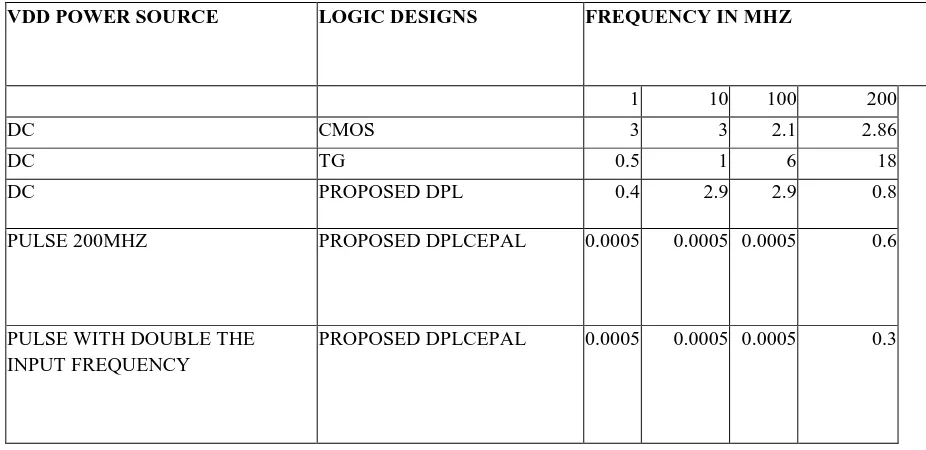
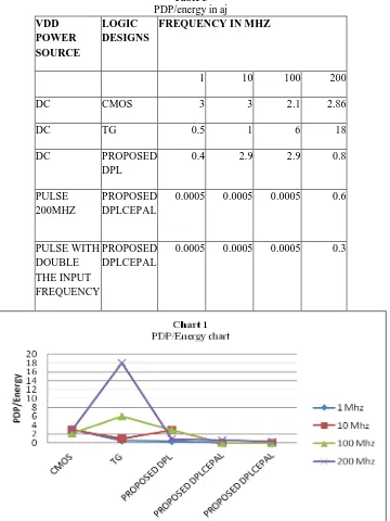
Table 1
Average power (vdd = 0.7v, vt = 0.3v) of various full adders in nano-watt.
VDD POWER
SOURCE
LOGIC DESIGNS
FREQUENCY IN MHZ
1 10 100 200
DC CMOS 12.14 118 1830 3420
DC TG 8.31 154.4 1560 3050
DC PROPOSED DPL
115.7 1780 18860 33890
PULSE 200MHZ PROPOSED DPLCEPAL
1500 4790 17870 29990
PULSE WITH DOUBLE THE INPUT FREQUENCY
PROPOSED DPLCEPAL
1820 2610 4990 6230
Delay TD is recorded for Sum as shown in following TABLE 2.
The delay of proposed design is superior to the existing CMOS adiabatic logics. From these tables the PDP/energy is calculated using the equation (4).
Table 3 shows PDP/Energy in Aj.
Table 2
Dealy Td for sum in nanosec.
VDD POWER SOURCE LOGIC DESIGNS FREQUENCY IN MHZ
1 10 100 200
DC CMOS 3 3 2.1 2.86
DC TG 0.5 1 6 18
DC PROPOSED DPL 0.4 2.9 2.9 0.8
PULSE 200MHZ PROPOSED DPLCEPAL 0.0005 0.0005 0.0005 0.6
PULSE WITH DOUBLE THE INPUT FREQUENCY
Sunil Jadhav
et al
, International Journal of Computer Science and Mobile Applications,
Vol.3 Issue. 6, June- 2015, pg. 12-20
ISSN: 2321-8363
©2015, IJCSMA All Rights Reserved, www.ijcsma.com 18
From Table 3 it is clear that the PDP/energy is the lowest for pulse power clock frequency 200MHZ and when the pulse power clock frequency is double the input frequency. This shows that energy consumption is lowest when frequency of power clock is double the input frequency which is superior to the old adiabatic concepts. This is shown graphically in Chart 1.
Table 3 PDP/energy in aj VDD
POWER SOURCE
LOGIC DESIGNS
FREQUENCY IN MHZ
1 10 100 200
DC CMOS 3 3 2.1 2.86
DC TG 0.5 1 6 18
DC PROPOSED DPL
0.4 2.9 2.9 0.8
PULSE 200MHZ
PROPOSED DPLCEPAL
0.0005 0.0005 0.0005 0.6
PULSE WITH DOUBLE THE INPUT FREQUENCY
PROPOSED DPLCEPAL
0.0005 0.0005 0.0005 0.3
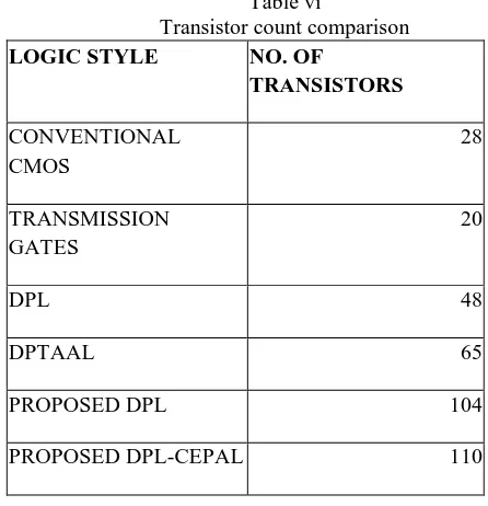
In our readings, it shows best result if the frequency of pulsed power source is double the input frequency. At last, the Transistor count comparison is shown in Table 4. As per the Moore’s law the transistor count per sqaure inch doubles every year and it is quite evident in our design.
Sunil Jadhav
et al
, International Journal of Computer Science and Mobile Applications,
Vol.3 Issue. 6, June- 2015, pg. 12-20
ISSN: 2321-8363
©2015, IJCSMA All Rights Reserved, www.ijcsma.com 19
Table vi
Transistor count comparison
LOGIC STYLE NO. OF
TRANSISTORS
CONVENTIONAL CMOS
28
TRANSMISSION GATES
20
DPL 48
DPTAAL 65
PROPOSED DPL 104
PROPOSED DPL-CEPAL 110
7. Conclusions and future scope
From Table 3 and chart 1 and we can conclude that energy consumption is lowest DPL-CEPAL logic when pulse clock frequency is 200MHZ and pulse power clock frequency is double the input frequency.
Thus, results show the best performance of proposed DPL-CEPAL logic as compared to the conventional techniques.
Hence we can conclude that the proposed DPL-CEPAL logic is fully adiabatic logic and it is implemented successfully in our design.
7.1 Future scope
The proposed design can be tested for low on chip power density further. Though we have utilized the pulsed power source efficiently, propagation delay can further be reduced by more efficiently utilizing the pulsed power supply as VDD source. Further the performance of proposed schematic may be increased by checking noise margin and current at different nodes.
IC layout can be created by importing spice net list of the proposed schematic and LVS comparison is possible to compare the schematic design and IC layout.
References
[1] Asynchronous Design of Energy Efficient Full Adder, 978-1-4673-2907-1/13/$31.00 ©2013 IEEE.
[2] Complementary Energy Path Adiabatic Logic based Full Adder Circuit, World Academy of Science, Engineering and Technology Vol:6 2012-06-24.
[3] Design of Low Power Multiplier with Energy Efficient Full Adder Using DPTAAL, Hindawi Publishing Corporation VLSI Design Volume 2013, Article ID 157872.
[4] Two New Low-Power and High-Performance Full Adders, JOURNAL OF COMPUTERS, VOL. 4, NO. 2, FEBRUARY 2009.
[5] A.Kishore Kumar, D.Somasundareswari, V.Duraisamy and M.Pradeepkumar, “Low power multiplier design using complementary pass-transistor asynchronous adiabatic logic,” International Journal on Computer Science and Engineering, Vol. 02, No.07, pp.2291-2297, 2010.
[6] Jianping Hu, Tiefeng Xu and Hong Li, “A lower power register file based on complementary pass-transistor adiabatic logic,” IEICE Trans. on Inf. & Sys, Vol.E88-D (7), pp. 1479-1485, 2005.
[7] Dai Jing. Hu Jianping, Zhang Weiqiang, Wang Ling, “Adiabatic CPL circuits for sequential logic systems,” in Proc. IEEE MWSCAS’06, pp.713-717, August 2006.
Sunil Jadhav
et al
, International Journal of Computer Science and Mobile Applications,
Vol.3 Issue. 6, June- 2015, pg. 12-20
ISSN: 2321-8363
©2015, IJCSMA All Rights Reserved, www.ijcsma.com 20
[9] M. Aguirre Hernandez and M. Linares Aranda, “A low-power bootstrapped CMOS full adder,” in Proc. of CIE, Mexico, pp.243–246, Sep.2005.
[10] Ilham Hassoune and Denis Flandre, “ULPFA: A new efficient design of a power-aware full adder,” IEEE Trans. Circuits and Systems, Vol. 57, No. 8, pp. 2066–2074, August 2010.