Manuscript History:
Received 29 July, 2015, Revised 2 September, 2015, Accepted 10 September, 2015, Published 30 September, 2015
The Impact of Soft Error on C-Elements Due to Process Corner Variation
and Temperature
Norhuzaimin Julai
Department of Electrical and Electronics, Universiti Malaysia Sarawak, Kota Samarahan
Sarawak, Malaysia. Email: [email protected]
Abstract
This paper presents current injection resemble single event upset (SEU) current at the vulnerable nodes on different configurations of C-elements under two different scenarios: process corner and temperature. The objectives are to identify the vulnerable nodes due to SEU and to find the critical charges needed to flip the output from low to high (0-1) and high to low (1-0) on different configurations of C-elements. The comparisons of C-elements in term of the resistivity toward soft error are presented.
Keywords: Soft Error,Process Variation, Temperature.
1. Introduction
Advancement in silicon technology has resulted in transistors becoming smaller which has in turn lowered operating voltage and capacitance [1]. Therefore, these transistors are more sensitive toward radiation-induced errors. As the demand for low power applications for digital electronics devices with high density continues to increase, the radiation effect on such electronic devices is becoming significant. Even though soft error due to radiation is not a permanent error, this type of error can cause data to be corrupted.
In this paper, the current pulse causing SEU is injected into different nodes of different C-elements. The amplitude of the current is increased until the output of the C-element is changed. Different configurations of C-elements are compared in terms of the charges needed to flip the output from 0-1 change or 1-0 change. The minimum charge needed to cause state change is known as the critical charge.
2. Single Event Upset
(a)
(b)
(c)
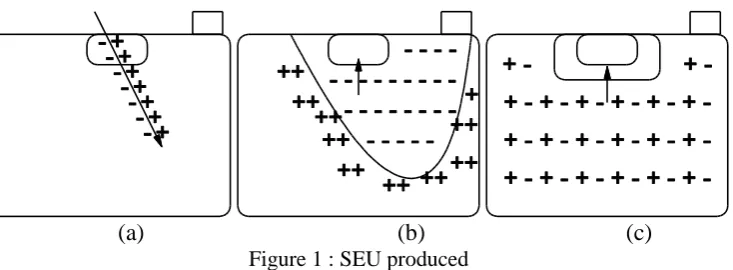
Figure 1 : SEU producedThe responses of the state holders can be categorized into three states:
a) No change to the state holder – There is insignificant output pulse that has been generated and does not cause any state change. It is assumed that if the generated pulse is less than 20% [4] of the input pulse such pulse can be further attenuated in the following gates and caused no further damage. This is shown in Figure 2(a) and Figure 3(a).
b) Pulse output is generated- Over a small range of input pulse amplitude, the pulse output is generated. It is assumed that if the generated pulse is 20% [4] or more of the input pulse, such pulse can be very likely to cause the problem. This is shown in Figure 2(b) and Figure 3(b) c) State change – At certain amplitude of current pulse, the state holder can change its state. This
is shown in Figure 2(c) and Figure 3(c)
Figure 2: State holder change from low to high (0-1)
Figure 3: State holder change from high to low (1-0)
3. Methodology
The workflow of the analysis is summarized below.
Step 2: Modelling the circuit. In order to compare different configuration of C-elements against SEU, the circuits are modelled to have the same width of the main transistors and the feedback transistors. For this purpose, CADENCE UMC90nm technology is used in the simulation.
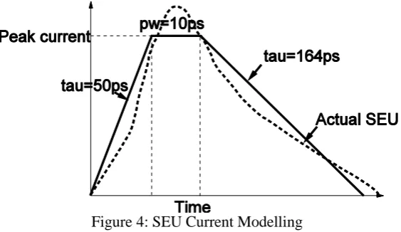
Figure 4: SEU Current Modelling
Step 3: Identifying the vulnerable nodes. The current pulses are injected at the main transistors and the output of the circuit is shown by Figure 5.
Step 4: Identifying the sources of variation. The sources of variations in the analysis are process corner and temperature. Five different process corners are TT(typical-typical), SS(slow PMOS and NMOS), FF(fast NMOS and PMOS), SNFP(slow NMOS and fast PMOS) and FNSP(fast NMOS and slow PMOS). It is assumed these parameters are Gaussian and mutually independent.
Step 5: Set inputs A=1,B=0. Repeat A=0,B=1. Assuming two inputs are A and B. There are two possibilities combination of input: A=1,B=0 and A=0, B=1. For each combination of input, there are two possibilities transition of output: High (1) to Low (0) and Low (0) to high (1).
Inputs Outputs
A=1,B=0 0-1
1-0
A=0,B=1 0-1
1-0
Step 6: Varying the amplitude of SEU current. As mentioned in step 1, the rising and falling times of the current pulse is fixed. However, in order to change the area under the curve, the amplitude is varied until the output is flipped. The simulation is done using circuit analyser (spectre).
Step 7: Identifying the amplitude of SEU Current that causes State Change. The amplitude of the current pulse is increased until the output is flipped at different nodes, different C-elements and different source of variation.
Step 8: Calculating critical charge. The critical charge which corresponds to the amplitude of the current pulse that causes the state to change is obtained at different nodes, different C-elements and different source of variations.
4. C-Element Modelling
Three different implementations of C-elements are used in the analysis:
(a) Single Rail with Inverter Latch SIL
(b) Single Rail with Conventional Pull-up Pull-down SC (c) Single Rail Symmetric Implementation SS
In order to make a fair comparison between different types of C-elements, the general sizes of the transistors are as follows:
a) The ratio of PMOS and NMOS for the main transistors is 1.125. This is consistent with Faraday Library for 90 nm technology.
b) The ratio between the main transistor and feedback transistor is 4:1
The analyses are subjected to the following assumptions:
a) The current pulse is assumed to hit the middle of the drain of the Off PMOS or NMOS transistor. The worst-case scenario is compared with different implementation of C-elements towards SEU. Thus, the values might be different to the actual experiments
b) The current pulse is assumed to resemble trapezoidal shapes with fast rising time and slow falling time and with maximum amplitude.
Current pulse is injected at different nodes for different configurations of C-elements. The purpose of the experiment is to find the charge needed to flip the output at the sensitive nodes due to the injected SEU under two variables
a) Process corner variation: Five different process corners are varied: TT, SS, FF, SNFP and FNSP.
b) Temperature variation: Temperature is varied from to taking only 4 distinct
points ( , , and ).
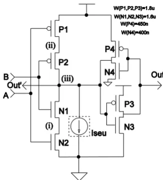
Figure 5: Current injection for SIL configuration
feedback is weaker so that it can be overpowered by the main pull up and pull down transistors. Suppose both inputs A and B are low causing the main pull up transistors to change the output Out to low. Similarly, if both inputs A and B are high causing the main pull down transistors to change the output Out to high. If the inputs are not equal, transistors P1 and P2 are disconnected from the power supply and transistors N1 and N2 are disconnected from the ground. The state of output Out is maintained by feedback inverters. Current pulse is injected at node (iii) as shown by the dashed box and the state change at node Out is observed. The experiments are repeated at nodes (i) and (ii). If A=0, B=1, node (ii) is connected to voltage supply, and therefore the charge needed to change the state are much higher compared with node (i). Similarly, if A=1,B=0 node (i) is connected to ground, and therefore the charge needed to change the state are much higher compared with node (ii). Therefore, node (ii) and node (i) are ignored in the analysis for A=0, B=1 and A=1,B=0 respectively.
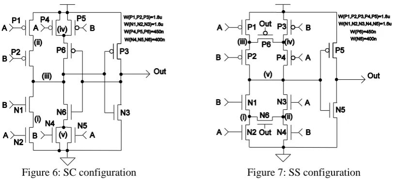
Figure 6: SC configuration Figure 7: SS configuration
A single rail with conventional pull-up pull-down configuration (SC) circuit consists of main pull up transistors (P1,P2), pull down transistors (N1,N2), inverter (P3,N3) and feedback transistors (P4,P5,N4,N5) as shown in Figure 6 [9]. Suppose both inputs A and B are low causing the pull up transistors to change the output Out to low. Similarly, if both inputs A and B are high cause the pull down transistors to change the output Out to high. If the inputs are not equal, transistors P1 and P2 are disconnected from the power supply and transistors N1 and N2 are disconnected from the ground. The weak feedback transistors (P6, N6) are activated via transistors (P4, N4) or (P5, N5) to maintain the output value. Current are injected at nodes (i), (ii) and (iii) and the state change at node Out is observed. Node (iv) and node (v) are not injected with current as these nodes connected to voltage supply and ground respectively when . Therefore bigger charges are needed to change the output from low to high and high to low. For the purpose of charge analysis, node (iv) and node (v) are excluded as the charge needed to change the state are much higher compared with node (i),(ii) and (iii). If A=0, B=1, node (ii) is connected to voltage supply, and therefore the charge needed to change the state are much higher compared with node (i). Similarly, if A=1,B=0 node (i) is connected to ground, and therefore the charge needed to change the state are much higher compared with node (ii). Therefore, node (ii) and node (i) are ignored in the analysis for A=0, B=1 and A=1,B=0 respectively.
A single rail symmetric configuration (SS) is similar to SC implementation. It consists of main pull up transistors (P1,P2,P3,P4), pull down transistors (N1,N2,N3,N4), inverter (P5,N5) and feedback transistors (P6,N6) as shown in Figure 7 [10]. The symmetrical structure gives an advantage with respect to the speed that due to the symmetrical design. Suppose both inputs A and B are low cause the pull up transistors to change the output Out to low. Similarly, if both inputs A and B are both high causing the pull down transistors change the output Out to high. If the inputs are not equal, and
either transistors N1, N6, N4 or transistors N2, N6, N3. Current is injected at nodes (i), (ii), (iii), (iv) and (v) and the state change at node Out is observed. If A=0, B=1, node (iii) is connected to voltage supply and node (ii) is connected to ground, and therefore the charge needed to change the state are much higher compared with node (i) and (iv). Similarly, if A=1,B=0 node (i) is connected to ground and node (iv) is connected to voltage supply, and therefore the charge needed to change the state are much higher compared with node (ii) and (iii). Therefore, node (ii) and node (iii) are ignored in the analysis for A=0, B=1 and node (i) and (iv) are ignored for A=1,B=0 respectively.
5. Result and Discussion
5.1. Critical charge at different vulnerable nodes
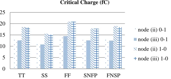
Five different process corner variations are performed and the charges needed to change the state of each process are compared. To observe the change in critical charge with respect to the process variations, the temperature is set at and the voltage supply is set at 1 V. As expected, the SS corner yields the smallest critical charge and the FF corner yields the highest critical charge. The highest critical charges of the FF process are due to the larger pull up and pull down strength of transistors. As a result, the strength of transistors give better stabilization in the voltage level of the storage node and hence higher critical charge is needed to flip the output [11]. Figure 8(a) shows the critical charge when inputs A=1, B=0 and Figure 8(b) shows the critical charge when inputs A=0, B=1. The critical charge at nodes (ii), (iii) of 0-1 is lower than node (ii) and (iii) of 1-0 change when A=1, B=0. Similarly, the critical charge at nodes (i), (iii) of 0-1 is lower than node (i) and (iii) of 1-0 change when A=0, B=1. The factor variations of critical charges between the extreme process corner variations are between 1.26X to 1.39X when inputs A=1, B=0 and 1.28X to 1.47X when inputs A=0, B=1, depending on the location of the SEU. The critical charges for TT, SNFP and FNSP are statistically equal since the standard deviation are 0.42f and 0.33f compared with the standard deviation of SS and FF which are 4f and 2.89f when inputs A=1, B=0 and inputs A=0, B=1 respectively. Thus, the critical charges for TT, SNFP and FNSP do not differ much
0 5 10 15 20 25 30 35
TT SS FF SNFP FNSP
Critical Charge (fC)
node (ii) 0-1 node (iii) 0-1 node (ii) 1-0 node (iii) 1-0
0 5 10 15 20 25 30 35
TT SS FF SNFP FNSP
Critical Charge (fC)
node (i) 0-1 node (iii) 0-1 node (i) 1-0 node (iii) 1-0
Figure 8(b): Process Corner Variation for SIL configuration (A=0, B=1)
In the SNFP corner, PMOS transistors have relatively stronger current compared with NMOS transistors and in the FNSP corner, NMOS transistors have relatively stronger current compared with PMOS transistors. However, the stronger PMOS or NMOS transistors counter balances the weaker NMOS or PMOS transistors and hence produce a comparable critical charge compared with the TT corner. These findings suggested that, in general, for the SIL configuration, critical charges are sensitive to process corner variations in particular the process corners SS and FF. Generally, as temperature increases, it degrades the threshold voltage, carrier mobility and saturation velocity [12]. As a result of degrading carrier mobility, the drain current becomes lower and the sensitivity of the node towards SEU is increased. Hence, the critical charge needed to flip the output is decreased. To observe the change in temperature variations, the process corner is set to TT and the voltage supply is set to 1 V. The result is shown in Figure 9(a) and 9 (b). The critical charges decrease by 11.3% for 0-1 change and 19.1% for 1-0 change when inputs A=1, B=0 as the temperature increases from to . Similarly when inputs A=0, B=1 the critical charges decrease by 9% for 0-1 change and 17.6% for 1-0 change on the same temperature increment. From the percentage change of the critical charge as above for 0-1 change and 1-0 change, it is concluded that PMOS transistors have a greater effect on temperature variation than NMOS. By increasing temperature, the mobility of holes is decreased more than the electron due to the critical electric field for holes decreasing more than the critical electric field for the electron. This is proven by the author in [12] that suggested the mobility of PMOS is reduced more than the mobility of NMOS at a temperature of for 65nm technology.
15 20 25 30
-40 10 60
Crit
ica
l C
ha
rg
e
(f
C)
Temperature (C)
node (ii) 0-1 node (iii) 0-1 node (ii) 1-0 node (iii) 1-0
15 17 19 21 23 25 27 29 31
-40 10 60
C
r
it
ic
a
l
C
h
a
r
g
e
(
fC
)
Temperature (C)
node (i) 0-1 node (iii) 0-1 node (i) 1-0 node (iii)1-0
Figure 9(b): Temperature Variation for SIL configuration (A=0, B=1)
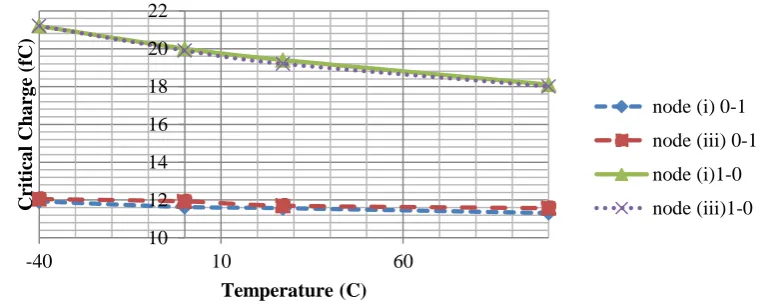
The critical charge when inputs A=1, B=0 and when inputs A=0, B=1 are shown in Figure 10(a) and 10(b) respectively. The critical charge 0-1 is lower than critical charge of 1-0 change for both combinations of inputs. The factor variations of critical charges between the extreme process corner variations are between 1.27X to 1.38X when inputs A=1, B=0 and 1.30X to 1.41X when inputs A=0, B=1, depending on the location of the SEU. The critical charges for TT, SNFP and FNSP are statistically equal since the standard deviation are 0.05f and 0.1f compared with the standard deviation of SS and FF which are 1.85f and 1.97f when inputs A=1, B=0 and inputs A=0, B=1 respectively. Thus, the critical charges for TT, SNFP and FNSP do not differ much.
0 5 10 15 20 25
TT SS FF SNFP FNSP
Critical Charge (fC)
node (ii) 0-1 node (iii) 0-1 node (ii) 1-0 node (iii) 1-0
0 5 10 15 20 25
TT SS FF SNFP FNSP
Critical Charge (fC)
node (i)1-0 node (iii)1-0 node (i)0-1 node (iii) 0-1
Figure 10(b): Process Corner Variation for SC configuration (A=0, B=1)
10 12 14 16 18 20 22
-40 10 60
Crit ica l C ha rg e (f C) Temperature (C)
node (ii) 0-1 node (iii) 0-1 node (ii) 1-0 node (iii) 1-0
Figure 11(a): Temperature Variation for SC configuration (A=1, B=0)
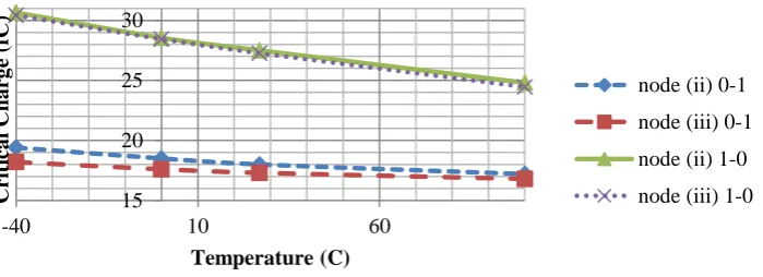
For the temperature change as shown by Figure 11(a) and 11(b), the critical charges decrease by 7.4% for 0-1 change and 18.6% for 1-0 change when inputs A=1, B=0 as the temperature increases from to . Similarly when inputs A=0, B=1 the critical charges decrease by 5.2% for 0-1 change and 14.6% for 1-0 change on the same temperature increment.
10 12 14 16 18 20 22
-40 10 60
Crit ica l C ha rg e (f C) Temperature (C)
node (i) 0-1 node (iii) 0-1 node (i)1-0 node (iii)1-0
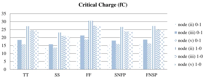
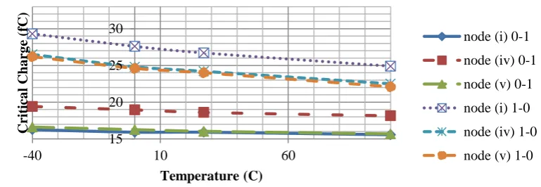
The critical charge when inputs A=1, B=0 and when inputs A=0, B=1 are shown in Figure 12(a) and 12(b) respectively. The critical charge 0-1 is lower than critical charge of 1-0 change for both combinations of inputs. The factor variations of critical charges between the extreme process corner variations are between 1.31X to 1.38X when inputs A=1, B=0 and 1.31X to 1.37X when inputs A=0, B=1, depending on the location of the SEU. The critical charges for TT, SNFP and FNSP are statistically equal since the standard deviation are 0.21f and 0.2f compared with the standard deviation of SS and FF which are 2.55f and 2.51f when inputs A=1, B=0 and inputs A=0, B=1 respectively. Thus, the critical charges for TT, SNFP and FNSP do not differ much. For the temperature change as shown by Figure 13(a) and 13(b), the critical charges decrease by 4.29% for 0-1 change and 17.5% for 1-0 change when inputs A=1, B=0 as the temperature increases from to . Similarly when inputs A=0, B=1 the critical charges decrease by 5.9% for 0-1 change and 15.65% for 1-0 change on the same temperature increment.
0 5 10 15 20 25 30 35
TT SS FF SNFP FNSP
Critical Charge (fC)
node (ii) 0-1 node (iii) 0-1 node (v) 0-1 node (ii) 1-0 node (iii) 1-0 node (v) 1-0
Figure 12(a): Process Corner Variation for SS configuration (A=1, B=0)
0 10 20 30 40
TT SS FF SNFP FNSP
Critical Charge (fC)
node (i) 0-1 node (iv) 0-1 node (v) 0-1 node (i) 1-0 node (iv) 1-0 node (v) 1-0
15 20 25 30
-40 -20 0 20 40 60 80 100
Crit
ica
l C
ha
rg
e
(f
C)
Temperature (C)
node (ii) 0-1 node (iii) 0-1 node (v) 0-1 node (ii) 1-0 node (iii) 1-0 node (v) 1-0
Figure 13(a): Temperature Variation for SS configuration (A=1, B=0)
15 20 25 30
-40 10 60
Crit
ica
l C
ha
rg
e
(f
C)
Temperature (C)
node (i) 0-1 node (iv) 0-1 node (v) 0-1 node (i) 1-0 node (iv) 1-0 node (v) 1-0
Figure 13(b): Temperature Variation for SS configuration (A=0, B=1)
5.2. Comparison of standard deviation of critical charges
variation. These showed PMOS transistors are more sensitive to the change of temperature compared with NMOS transistors.
0 0.5 1 1.5 2 2.5 3
1
.0
0
E
-15
Figure 14(a):Standard Deviation with respect to Process (A=1,B=0)
0 0.5 1 1.5 2 2.5 3
1
.0
0
E
-15
Figure 14(b):Standard Deviation with respect to Process (A=0,B=1)
0 0.5 1 1.5 2 2.5
1
.0
0
E
-15
0 0.5 1 1.5 2 2.5
1
.0
0
E
-15
Figure 15(b):Standard Deviation with respect to Temperature (A=0,B=1)
6. Conclusions
Soft error affects digital circuit by corrupting the data in the circuit. In this paper, current pulse causing SEU is injected to every nodes of different implementation of C-elements. The factors that we used as a variable in the simulation are process corner and temperature. Each of the variables is varied and the critical charge needed to change the state is obtained. For process corner, FF gives the highest critical charges due to the larger pull up and pull down strength of transistors. As a result, the strength of transistors give better stabilization in the voltage level of the storage node and hence higher critical charge is needed to flip the output. For temperature, as temperature increases, it degrades the threshold voltage, carrier mobility and saturation velocity [12]. As a result, the drain current becomes lower and the sensitivity of the node towards SEU is increased. Hence, the critical charge needed to flip the output is decreased. It is observed that process corner is the most important factors of critical charge variation since it has the highest standard deviation compared with temperature. It is also observed that the standard deviations for SIL are the highest compared with other single rail configurations (SS and SC) since it has the least number of transistors.
References
.[1] Rajaraman Ramanarayanan, Ramakrishnan Krishnan, Vijaykrishnan Narayanan and Mary Jane Irwin, Modelling Soft Errors at the Device and Logic Levels for Combinational Circuits, IEEE Transactions on Dependable and Secure Computing, Vol 6, No 3, 2009.
[2] Fan Wang and Vishwani D. Agrawal, Single Event Upset: An Embedded Tutorial, 21st International Conference on VLSI Design, 2008, pp 429 – 434.
[3] Anghel, M.Rebaunger, M.Sonze Reorda and M.Violante, Multi-Level Fault Effects Evaluation, Radiation Effects on Embedded Systems,Springer, 2007, pp. 69-88
[4] Gottfried Fuchs, Matthias Fugger and Andreas Steininger, On the Threat of Metastability in an
Asynchronous Fault-Tolerant Clock Generation Scheme, Fault-Tolerant Distributed Algorithms on VLSI Chips
[5] Weidong Kuang, Ibarra C.M and Peiyi Zhao, Soft Error Hardening for Asynchronous Circuits ,22nd IEEE International Symposium on Defect and Fault Tolerance in VLSI Systems, 2007, pp 273-281.
[6] Hungse Cha and Janak H. Patel, A Logic Level Model for Alpha Particle Hits in CMOS Circuits, International Conference on Computer Design, October 1993, pp 538-542.
[7] V.A. Carreno and G Choi, R.K Layer, Analog-Digital Simulation of Transient-Induced Logic Errors and Upset Susceptibility of an Advanced Control System, NASA Technical Memorondum 4241, Nov 1990. [8] A. J. Martin, Formal Program Transformations for VLSI Circuit Synthesis, Formal Development of
Programs and Proofs (E. W. Dijkstra, ed.), UT Year of Program- ming Series, pp. 59-80, Addison-Wesley, 1989
[10]K. van Berkel, Beware the Isochronic Fork, The VLSI journal, Vol. 13, pp. 103-128, June 1992 [11]Tino Heijmen et al, A Comparative Study on the Soft-Error Rate of Flip-Flop from 90-nm production
Libraries, 44th IEEE International Symposium on Reliability Physics, March 2006, pp. 204-211.
[12]Kumar, R and Kursun, V, Impact of Temperature Fluctuation on Circuits Characteristics in 180nm and 65 nm CMOS Technologies, International Symposium on Circuits and Systems, 2006, pp. 3858-3861.
Author
Norhuzaimin Julai