Available Online At www.ijpret.com
INTERNATIONAL JOURNAL OF PURE AND
APPLIED RESEARCH IN ENGINEERING AND
TECHNOLOGY
A PATH FOR HORIZING YOUR INNOVATIVE WORKDISCRETE WAVELET TRANSFORM, IMAGE SCRAMBLING, ARNOLD TRANSFORM
VEENA GAONKAR, H. G. VIRANI
Dept of Electronics and Telecommunication, Goa College of Engineering, Farmagudi, Goa, India.
Accepted Date:
27/02/2013
Publish Date:
01/04/2013
Keywords
Image processing,
Printed circuit Board,
Defect detection,
Defect classification
Corresponding Author Ms. Veena Gaonkar
Abstract
A variety of ways has been established to detect defects on
printed circuit boards (PCBs), but it is also crucial to classify
these defects in order to analyze and identify the root causes
of the defects. This paper proposes a PCB defect detection
system by incorporating proper image registration and noise
elimination procedure to solve the alignment and uneven
illumination problem. Resultant output of defect detection
stage is further used for classification process.
Classification system is improved by combining image
segmentation algorithm [1] and image processing theories [2].
Based on initial studies, some PCB defects can only exist in
certain groups. Thus, it is obvious that the image processing
algorithm could be improved by applying a segmentation
exercise which helps to increase the number of groups and
Available Online At www.ijpret.com INTRODUCTION
Visual inspection is generally the
largest cost of PCB manufacturing. It is
responsible for detecting both cosmetic
and functional defects and attempts are
often made to ensure 100% quality
assurance for all finished products. There
are two main processes in PCB inspection:
defect detection and defect classification.
It is important to note that the previously
proposed algorithms did not take into
account the image registration problem
[4] as a result; the image still could be
interfered by unwanted noise due to
slightly misalignment and uneven
binarization. Hence, it is difficult to reduce
or diminish the noise in the output image.
Based on this deficiency of defect
detection, the results obtained in defect
classification stage will be also inaccurate.
Hence defect classification algorithm is
improved by incorporating proper image
Registration and noise elimination
technique to solve the alignment and
uneven illumination problem.
Currently there are many algorithms
developed for PCB defect detection, using
contact or non contact methods. Contact
method tests the connectivity of the
circuit but is unable to detect major flaws
in cosmetic defects such as mouse-bite or
spurious copper and is very
setup-sensitive. Any misalignment can cause the
test to fail completely. Non contact
methods can be from a wide range of
selection from x-ray imaging, ultrasonic
imaging, thermal imaging and optical
inspection using image processing [3].
Although these techniques are successful
in detecting defects, none is able to
classify the defects. This project utilizes a
non-contact reference based, image
processing approach for defect detection
and classification.
DEFECTS
PCB defects can be categorized into two
groups; functional defects and cosmetic
defects. Functional defects can seriously
affect the performance of the PCB or
cause it to fail. Cosmetic defects affect the
appearance of the PCB, but can also
jeopardize its performance in the long run
due to abnormal heat dissipation and
distribution of current. There are 14
known types of defects for single layer,
Available Online At www.ijpret.com TABLE I: Defect on Single Layer Bare
PCB
No. Defect
1 Breakout
2 Pin-hole
3 Open Circuit
4 Under-etch
5 Mouse-bite
6 Missing Conductor
7 Spur
8 Short
9 Wrong Size Hole
10 Conductor Too Close
11 Spurious Copper
12 Excessive Short
13 Missing Hole
14 Over-etch
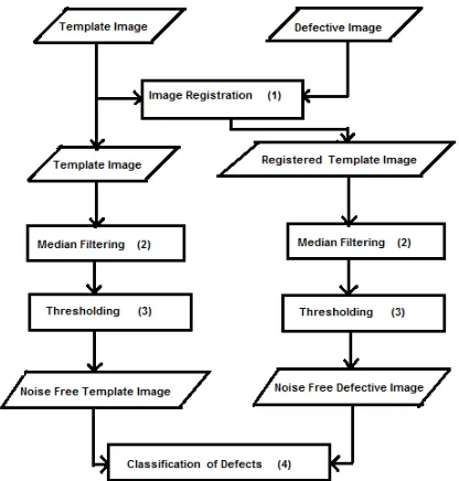
III. THE IMPROVED PCB INSPECTION SYSTEM
Figure 1 depicts the PCB inspection
system developed in this research for
detecting and classifying defects on PCB
which includes four major stages. The
stages are:
Stage 1:Image registration process-- The
image registration process is an important
stage in inspecting real PCB images. Image
registration can be broadly
Fig 1. Flow chart of the improved PCB
inspection system defined as the process
of finding a transformation that aligns one
image to another. In this research,
geometric transformation is used to find a
transformation that aligns a template
image and a defective image.
Stage 2: Median filtering-- In acquisition
processing of images, due to input
conversion apparatuses and influences of
ambient environment, obtained digital
images will contain many kinds of noises,
which interfere with the useful
information in post-processing and result
in information loss or misidentification.
We choose median filtering to improve
image quality, and median filtering can
efficiently inhibit noises in images and
Available Online At www.ijpret.com Stage 3: Thresholding-- The output of the
thresholding operation is a binary image
whose one state will indicate the
foreground objects and whose
complementary state will correspond to
the background. To separate the
foreground and background in an image,
the correct threshold value must be
found. Several different methods for
choosing a threshold exist; users can
manually choose a threshold value, or a
thresholding algorithm can compute a
value automatically, which is known
as automatic thresholding .
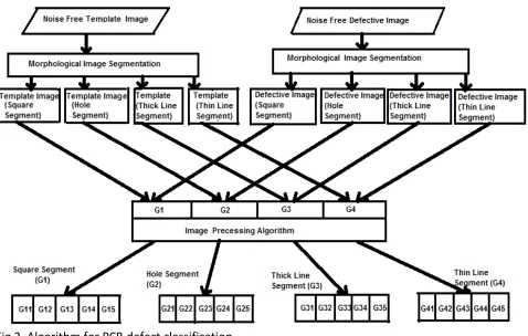
Stage 4: The classification of defects—
Noise free template and defective
images are fed into the image
segmentation algorithm to separate PCB
images into four main segments which are
square segment, hole segment, thick line
segment and thin line segment using
mathematical morphology as shown in
figure 2.
Morphological process involves
techniques such as dilation, erosion,
opening and closing which helps in
partitioning the images and associates
certain types of defects with certain
patterns such as wrong size hole,
breakout and missing hole for hole
segment or missing conductor and open
circuit for thin-line segment. Other
defects might exist in multiple segments.
Image processing algorithm developed by
Khalid [2], to classify the 14 defects into
five groups. Those groups with the
respective defects are as follows:
Group1: missing hole, wrong size hole.
Group2: spur, short, spurious copper,
excessive short, conductor too close
Group3: open circuit, mouse bite,
overetch, conductor missing.
Group4: under etch.
Group5: pinhole and breakout.
By combining morphological image
segmentation and image processing
algorithms it is possible to classify the
defects into more number of groups and
also reduce the number of defects in each
group.
SIMULATION RESULTS
Two images are needed for the
inspection, the Template image and the
Defective image as shown in figure 3 and
Figure 4 respectively. The result of the
previous PCB inspection system has
indicated that without a proper
imageregistration operation, the PCB
inspection system is likely to totally fail.
Hence, theimproved PCB inspection
Available Online At www.ijpret.com imageregistration operation. The result of
image registration is shown in Figure 5.
Two gray-scale images are needed for this
operation, template image and a
defectiveimage as shown in Figures 3 and
5. However, the images may still feature
interference by unwanted noise due
toslight misalignment and uneven
binarization. To effectively eliminate the
noise, median filtering and thresholding
technique is used. Khalid’s classification
Fig 2. Algorithm for PCB defect classification
Available Online At www.ijpret.com Fig 4. Defective bare PCB image
Fig 5.Registered defective image
can be further improved by combining the
image segmentation algorithm developed
by Heriansyah[1] and image processing
algorithm developed by Khalid[ 2].Both the
images [figure 3 and figure 5 ]are
segmented into 4 segments each; square
segment, hole-segment, thick line segment
and thin-line segment. The image
processing algorithm is able to generate 4x5
images (20 images) which will improve the
overall defect classifi- cation ability of the
system by increasing the number of groups
from 5 to7 as listed in Table III. A sample of
result for a defective image consisting of
random defects is shown in figure 8.
Available Online At www.ijpret.com Fig 4. Defective bare PCB image
Fig 5.Registered defective image
can be further improved by combining the
image segmentation algorithm developed
by Heriansyah[1] and image processing
algorithm developed by Khalid[ 2].Both the
images [figure 3 and figure 5 ]are
segmented into 4 segments each; square
, thick line segment
line segment. The image
processing algorithm is able to generate 4x5
images (20 images) which will improve the
cation ability of the
system by increasing the number of groups
able III. A sample of
result for a defective image consisting of
random defects is shown in figure 8.
Fig 6. Morphological segmentation for Template Image
Fig 7:Morphological Segmentation for defective Image
TABLE III.Classified Group of Defects
No. Image Classified Defects
1 G14+G24 Underetch
2 G21 Wrong size hole, Missing
hole
3 G13+G23 Mouse bite, Overetch
4 G15+G25 Breakout,pinholes
5 G22+G32 Spur, Short, Spurious
copper, Excessive short
6 G42 Conductor too close
7 G43 Conductor Missing,Open
Circuit
Fig 6. Morphological segmentation for Template Image
Fig 7:Morphological Segmentation for
TABLE III.Classified Group of Defects
Classified Defects
Underetch
Wrong size hole, Missing hole
Mouse bite, Overetch
Breakout,pinholes
Spur, Short, Spurious copper, Excessive short Conductor too close
Available Online At www.ijpret.com G14 +G24 G21
G13+G23G15+G25
G22+G32 G42
G43
Fig 8.Sample Result of Defect Image
CONCLUSION
The improved PCB inspection system
incorporated with an image registration
operation to solve the alignment problem.
A noise elimination procedure is designed in
such a way that the resultant defects found
in this algorithm is more precised compare
to previous algorithm. Algorithm is also
successfully able to improve the image
processing algorithm developed by
Khalid[2] by increasing the classification of
14 defects from 5 to 7 groups.
However, the major limitation of this
algorithm is developed to work with binary
images only, whereas the output from the
cameras is in grayscale format. Although
the conversion can be made from grayscale
to binary format imperfection still can be
occurred. Thus, this algorithm should be
improved to handle the grayscale image
format. Future improvement for the
algorithm should include the ability to
detect and classify all 14 defects
individually.
REFERENCES
1. R. Heriansyah, S.A.R Al-attas, and M.M.
Ahmad Zabidi, CoGRAMM Melaka, Malaysia
(2002) “Segmentation of PCB Images into
Simple Generic Patterns using
Mathematical Morphology and Windowing
Technique”
2. Noor Khafifah Khalid, Zuwairie Ibrahim,
and MohamadShukriZainalAbidin - IJSSST,
Available Online At www.ijpret.com group defects on printed circuit board for
automated visual inspection”
3. Moganti, M.ERCAL, F. Dagli, C. H. and
Shou, Tsunekawa, 1996, 63,No2,
“Automatic PCB Inspection Algorithms:
A survey.
4. Ismail Ibrahim, Syed Abdul Rahman Syed
Abu Bakar, Musa Mohd Mokji, ICIC
international pp. 717-722(2012) “An Image
Registration technique to enhance PCB