Available Online At www.ijpret.com
INTERNATIONAL JOURNAL OF PURE AND
APPLIED RESEARCH IN ENGINEERING AND
FPGA BASED
M.
1. Professor &Head, ECE Dep India
2. Asst. Professor, ECE Dept.
Accepted Date: 29/12/2012 Publish Date: 01/01/2013 Keywords Channelizers, Polyphase, SATCOM, FDM, NCO, CRC, FEC, Guard band, ARQ, SCA Corresponding Author Mr. M.Harikrishna
Multiple communication channel support in RF transmission, such as that in a Software Defined Radio (SDR) warrants the us
extract required channels from the received RF frequency band and to perform follow
of channelization as it applies to low applications in wireless and
domains. Smaller bandwidths and changing requirements of bandwidth calls for a programmable channel selection mechanism whereby channels and the resulting bandwidth can be selected based on target application, which is the
systems. Evolving wireless standards, advances in FPGA technologies available at a much lower Non
those for a comparable custom designed ASIC make programmable ch
requirement for parts used in space systems. This paper addresses the importance of methods to meet radiation requirements: selection of robust technologies and hardening by design.
IJPRET-QR CODE
Available Online At www.ijpret.com
INTERNATIONAL JOURNAL OF PURE AND
APPLIED RESEARCH IN ENGINEERING AND
TECHNOLOGY
A PATH FOR HORIZING YOUR INNOVATIVE WORK
FPGA BASED POWER EFFICIENT CHANNELIZATION
M. HARIKRISHNA1,KUMAR KESHAMONI2,
ECE Dept. RVR Institute of Engineering and Technology
. RVR Institute of Engineering and Technology
Abstract
Multiple communication channel support in RF transmission, such as that in a Software Defined Radio (SDR) warrants the us
extract required channels from the received RF frequency band and to perform follow-on baseband processing. This paper describes the process of channelization as it applies to
low-applications in wireless and Satellite Communications (SATCOM) domains. Smaller bandwidths and changing requirements of bandwidth calls for a programmable channel selection mechanism whereby channels and the resulting bandwidth can be selected based on target application, which is the primary principle in the Software Defined Radio based systems. Evolving wireless standards, advances in FPGA technologies available at a much lower Non-Recurring Engineering (NRE) costs than those for a comparable custom designed ASIC make programmable channelizer a viable solution. Radiation hardness is an essential requirement for parts used in space systems. This paper addresses the importance of methods to meet radiation requirements: selection of robust technologies and hardening by design.
INTERNATIONAL JOURNAL OF PURE AND
APPLIED RESEARCH IN ENGINEERING AND
A PATH FOR HORIZING YOUR INNOVATIVE WORK
ATION FOR SDR
RVR Institute of Engineering and Technology, Hyderabad,
RVR Institute of Engineering and Technology, Hyderabad, India
Multiple communication channel support in RF transmission, such as that in a Software Defined Radio (SDR) warrants the use of channelizers to extract required channels from the received RF frequency band and to on baseband processing. This paper describes the process -power and high-efficiency Satellite Communications (SATCOM) domains. Smaller bandwidths and changing requirements of bandwidth calls for a programmable channel selection mechanism whereby channels and the resulting bandwidth can be selected based on target application, primary principle in the Software Defined Radio based systems. Evolving wireless standards, advances in FPGA technologies Recurring Engineering (NRE) costs than those for a comparable custom designed ASIC make programmable annelizer a viable solution. Radiation hardness is an essential requirement for parts used in space systems. This paper addresses the importance of methods to meet radiation requirements: selection of robust technologies and hardening by design.
Available Online At www.ijpret.com
INTRODUCTION
Software Controllable Architectures (SCA) is
more adaptable to multi-standard and
multi-channel communication systems.
FPGA based channelizers are essential
components and enable channel selection
to be configurable based on the end
application. The goal is to obtain maximum
use of a single design through software
reconfiguration of hardware assets and
dynamic configuration and selection of
channels, while ensuring highest level of
fidelity of signals received at the
destination.
Multiple access systems are widely used in
satellite and terrestrial communications
(such as JTRS land mobile radio), paving the
way for SDR, which promises
interoperability and compatibility among
disparate standards. The use of such
systems in SATCOM reduces the power
requirements and also allows frequency
reuse between the satellite beams.
Wideband and narrow band techniques are
two main categories. Power efficiency of
any of these techniques can be improved by
adding forward error correction coding
(FEC) with a bandwidth penalty and
improved bandwidth efficiency will be
become more and more relevant with
congested channels. This has to be achieved
without jeopardizing the data quality.
Systems have to be designed to coordinate
carrier frequency, phase and symbol timing.
Synchronous CDMA, orthogonal FDMA and
wavelet-packet multiple access are all
viable options [7, 31]. In this work, we will
concentrate on the critical aspects of
channelizer design itself, trade-offs for
low-power requirements, programmability,
implementation details and radiation
effects.
BACKGROUND
Channel Coding
The primary goal of channel coding is to
reduce impairments in a reconstructed
signal that was affected by transmission
errors and Automatic Repeat Request (ARQ)
to further improve channel conditions.
Various forms of channel coding are
employed in a transmitter including Cyclic
Redundancy Check (CRC) bits for error
detection and Forward error correction
(FEC) bits for error correction. These
Available Online At www.ijpret.com
programmable device from commercially
available FPGA vendors. For example, in the
CRC function, configurable parameters
include
- Variable length generator polynomial
- Variable data width from 1 to width of
polynomial
- Specified initial value
Channelizer
Several techniques in channelization are
suitable for RF communication channels
including Digital Down Conversion,
Polyphase Fast-Fourier Transform
(Polyphase FFT) Filter Banks and Frequency
Domain Filtering. A multichannel digital
receiver is used typically to down-convert a
set of frequency division multiplexed (FDM)
channels from a sampled data signal
stream. Conversely, a multichannel digital
transmitter simultaneously up-converts a
number of baseband signals to assemble a
set of FDM channels and send them into a
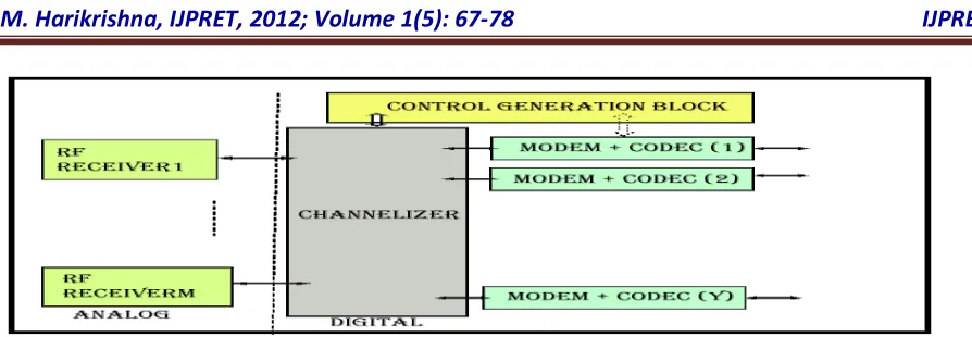
single data signal stream Figure 1 shows a
basic wideband transceiver. The system has
RF receivers on the front end which digitize
the input channels (for example, ten 20
MHZ channels). The frontend comprises of
Analog to Digital Conversion (ADC)
subsystem which forms the first part of the
digital transceiver. Analog signals are mixed
with locally generated signal, and band pass
filtered. In the process the received
wideband signal is split into quadrature
channels (I and Q) that is digitized. An IQ
balancer is generally used prior to the
channelizer or can be made a
subcomponent of the channelizer itself.
Each incoming channel is assigned a unique
Channel ID. The digitized channels are fed
to the channelizer which selectively extracts
desired channels and desired number of
channels. The digital section of the receiver
is called a channelizer or zero-IF
demodulator. The channelizer maps RF (or
near RF) directly to baseband. For
mobile/hand-held wireless applications for
which SDR is considered to be increasingly
suitable, a premium is also placed on power
Available Online At www.ijpret.com
Figure 1 Top level Functional Blocks in a
Transceiver
The extracted channels both control and
data portions are then post-processed in
channel processors for demodulation and
decoding of real data. During transmit, the
payload data is encoded and modulated
and then sent to the channelizer which
generates necessary channels for onward
transmission. The number of channel
processors (y) depends on the number of
active channels at the output of the
channelizer. For programmability, input
frequency, output channels and bandwidth
parameters can be set as desired, and can
be changed at any given time.
DESIGN TRADE-OFFS FOR CHANNELIZER
During Digital Down Conversion, convergent
rounding is used between stages to
minimize DC biases into the processed
output signal. The pre -processor in the
architecture under consideration is a
Hogenauer based Cascade Integrator Comb
(CIC) filter which can enable higher
decimation rate channelizations for higher
input data rate, when compared to a
conventional multiplier based mixer with
Direct Digital Synthesizer circuits. With CIC
filters, the preprocessing stage essentially
becomes Multiply Accumulate (MAC) free
low pass filter. This gives high signal
processing speeds. Post processing filter
which is normally needed in a CIC based
filter do not need to be at such high rate
and thus can be implemented with FIR
filters. Thus even by reducing the
complexity of design with use of CIC filters,
we still have to deal with high power
consumption due to the mixers and DDS
logic that is necessary in a DDC based
Available Online At www.ijpret.com
typically involves both FIR filters and a
numerically-controlled oscillator (NCO),
both of which are available as user
configurable intellectual property (IP) for
programmable logic users. For low-power
applications we found that DDC may not be
the best choice since it is also important to
decrease the complexity of arithmetic
operations in the Digital mixers and Direct
Digital Synthesizers (DDS) in order to
achieve lowest power. Without having to
deal with reducing the complexity of mixers
and DDS logic, it can be overcome by
“eliminating” the use of such components.
The same functionality can be however
gained by employing poly phase Fast
Fourier Transform (FFT) filter bank
segments that are multiplier-free [4, 9, 21,
and 24]. Polyphase FFT filtering is suited for
designs where (a) sampling rates that are
power of 2 times the baseband bandwidth
and (b) number of channels equal the
decimation rate. Although these
requirements make the flexibility of
channelizer parameters hard to achieve,
poly phase filter technique of
channelization is efficient in terms of less
area and less power. Polyphase filter banks
also lead to reduced cost because of fewer
system resources that are needed to
implement. Certain transformations in
terms of rearranging of functions can be
performed to the standard Polyphase FFT
based channelizer to achieve a modified
and more efficient channelizer as shown in
Figure 2.
In order to address the problem of full
complex heterodyne at the output of band
pass filter, we can utilize sample rate
reduction by retaining only one of M
samples if it is decimation by M, thus
enabling processing of only the retained
samples. We can also take advantage of the
fact that if we can select the center
frequencies which alias to a DC value, then
the entire heterodyne operation becomes a
Available Online At www.ijpret.com
heterodyne. Polyphase FFT filter bank
(PFFB) scheme assumes redundancy within
the frequency plan of wideband channel.
This scheme works best if the input consists
of identically shaped and equally spaced
channels. This mechanism requires one poly
phase FIR filtering component to isolate and
decimate various channels, followed by a
FFT computation block. The poly phase
segments can be made multiplier-free for
low power applications. One optimization
that has often been used in wireless
communications is quantizing the input
signal to such a level that it essentially
becomes like a band pass signal [4, 9, 30].
The heterodyne function is unnecessary,
since there is no need for mixing with
synthesized carrier as in DDC. Hence, there
is no need for a DDS. This has its limitations
in that the channel isolation is done on a
per channel basis. Advantages of polyphase
FFT over conventional window based FFT
methods also include resilience to strong
interference in pass band ripple and
spectral leakage After studying various
techniques to accomplish single or multiple
channel extraction of signal bands from the
bandwidth collected by high bandwidth
converters, a modified version of the base
polyphase system is chosen.
SYSTEM VIEW
FPGA technology provides the
signal-processing engineer with the ability to
construct a custom data path that is
tailored to the application at hand. FPGA
reconfigurable DSP system is shown in
Figure 3.
Figure 3 Reconfigurable DSP Systems
RADIATION EFFECTS IN VERY DEEP
SUB-MICRON (VDSM) CIRCUITS
(A)Cumulative Effects: Two different types
of cumulative effects, namely Total Ionizing
Dose (TID) effects that cause increase of
leakage currents, variation of transistor
threshold voltage, an increase of transistor
Available Online At www.ijpret.com
supply currents increase, the switching and
dynamic parameters degrade, and the noise
margins are reduced; and Displacement
Damage (DD) caused by high energy, is a
main concern for optoelectronics devices,
but it is not a concern for a CMOS devices.
(B)Single Event Effects (SEE): Prominent SEE
effects are
•Single Event Upset (SEU): The current
spike results of a bit flip in a memory cell or
a latch. The effect is permanent as long as
the correct information is not rewritten in
the memory cell.
•Multiple Events Upset (MEU): A single
particle causes an upset in several
neighboring memory cells.
•Single Event Latch-up (SEL): A low
resistivity path is triggered between Vdd and
Vss, and can destruct the chip if latch-up
current is high enough. A power cycle is
necessary to recover from a SEL condition.
•Single Event Transient (SET): A glitch
occurs that may propagate in the circuit
and cause errors.
•Single Event Functional Interrupt
(SEFI): This event affects state machines
and a circuit re initialization is necessary
to recover.
There are different ways to mitigate
radiation effects. The first method is to
work on the integrated circuits process. For
example, the quality of oxides is a main
driver for total dose hardness. For example,
CMOS/SOI technologies are immune to SEL.
In general, all CMOS processes with an
epitaxial layer are less prone to be sensitive
to SEL, and are less sensitive to MEU than
CMOS bulk processes. This, for example, is
the solution that Xilinx proposes for the
Aerospace applications. Xilinx space FPGAs
are processed with a special epitaxial layer
that makes them not sensitive to SEL.
Hardening by process may be very effective.
However, this approach is only accessible to
parts manufacturers. The only way for
design engineers to harden a circuit against
radiation effects is to perform hardening by
design. Hardening by design can be
performed at different levels:
• At the elementary transistor levels,
layout techniques and guard band
techniques improve the TID and SEL
tolerance. These techniques require the
development of a specific library and
can be quite time consuming.
Available Online At www.ijpret.com
techniques like triple module
redundancy, Error Detection and
Correction codes (EDAC), CRC frame
checks, and others can be very powerful
to mitigate SEE.
• Other design techniques include
complete initialization of state
machines, defining all possible states,
appropriate choice of state machine
implementation, adding redundant logic
(which has the downside of increasing
on-chip real estate).
Testing is an essential activity to assess
the sensitivity of a device to radiation
effects and will be performed at
specialized test facilities10.
DESIGN APPROACH
The overall objective of this work has been
to develop a low-power Channelizer design
that can be implemented on FPGA
device(s). The design consists of schematic
entry and RTL descriptions in Verilog.
Specific tasks include:
Step 1. Improvements of Polyphase
Channelizer Efficient M-Path Polyphase
channelization architecture is designed for
highly efficient and low-cost (power and
area) designs. For providing a complete
solution to the problem on hand, we need
to address two aspects: 1) Programmability
and 2) Low-Power and efficient design
techniques. In a channelizer design, we
need to perform basic channelization and
secondary signal processing operations. The
main functional blocks in a poly phase
system are shown in Figure 2, with down
conversion of the incoming channel with a
complex heterodyne, followed by a digital
low-pass filter and a down-sampling
operation as required by the decimator.
Low power, low weight techniques:
Reusability, software downloaded bit
streams save area, weight and package size.
Clocking biases conventionally have been
used to reduce dynamic power. Selective
operation of parts of the device is another
method that can save power dissipation. In
addition, Multi-layer, 3-D packaging
techniques are paving the way into
low-power and low weight implementations.
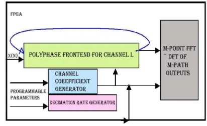
Resource sharing: It is clear from Figure 2
that the structure needed at the input of
the M-point FFT is similar to all channels,
except for channel co-efficient. These
Available Online At www.ijpret.com
the FPGA, separately for each channel and
passed to the FFT. Alternatively, the
coefficients for all channels can be
pre-calculated and loaded into a Content
Addressable Memory (CAM) in the FPGA.
The front-end processing units consisting of
commutator and poly phase segment is
grouped into what we are referring to as
“Polyphase Frontend”. Programmable
parameters include decimation rate,
channel Id, bandwidth and center
frequency, are supplied to Channel
Coefficient Generator (CCG) and Decimation
Rate Generator (DRG). This design is
capable of generating channel coefficients
and decimation rates that are unique to
each channel. The poly phase frontend is
recursively called M times to perform the
operation for M channels. Thus it has an
interesting and a much desirable byproduct
for programmable channelizers. We initially
noted that poly phase channelizers support
fixed set of frequency plans with equally
spaced channels. However, this design
enables us to overcome that obstacle thus
supporting multiple frequency plans with
the overhead of an extra FFT logic. Since
low-power is our criterion, the decrease in
speed due to this design is an acceptable
trade-off. This improved architecture is
shown in Figure 4.
Figure 4 Resources Sharing of Polyphase
Frontend Logic
Quantization: If accuracy of the data is not
paramount, quantization of input samples
prior to entering the poly phase section is
recommended. The poly phase filters are
multiplier-free since quantization leads to
approximations of multiplication
operations to basic additions and shift
operations. This also is a feasible approach
for low -power design, depending on
amount of accuracy needed.
Implementation related improvements
•Segmented routing is essential in high
performance and power efficient DSP based
designs. Some Xilinx and Altera FPGAs can
Available Online At www.ijpret.com
device utilization. Segmented routing
architectures also lead to lesser power and
are more predictable.
•Board space reduction is accomplished by
the use of a small outline Ball Grid Array
(BGA) package, which results in a small
footprint. In the case of FPGA based design,
there are several suitable devices from
vendors yielding efficient board designs.
The resource reduction translates into
lesser power. For a typical application there
can be resource savings of up to a factor of
20 by moving from a standard DDC based
approach to
Additional low-power design techniques
include
• Interleaving layout methods for CLBs
with VDD and VL , thus creating easy
access to power grid
• Higher Vt for SRAM intensive FPGA
device if chosen
• Fine tuning of transistor sizes in level
converter
• Gate-boosted power controlling
transistors in Figure 5.
• Clock gating to save dynamic power
for portions of design that are not
functional
Therefore, with the modified and
enhanced channelizer, configurable
parameters include Input frequency,
Number of output channels, Output
frequency bandwidth, Quantization
Enable (‘Q’ to enable or disable
quantization based on required accuracy
of data), Supply voltage Configuration bit
(‘S’ to choose between VDD and VL).
Step 2. Generate a computer simulation
model. Simulation model is developed in
Verilog for sub-components of the system.
A subtask of this step includes generation of
functional tests to verify the functionality.
Block level and system level tests, with
various configurations of programmable
parameters are vital part of functional
testing. This gives flexibility of modifying
the frequency plans of a wideband channel
and thus simulating different target
applications.
APPLICATIONS
The programmable channelizer can be used
for rapid prototyping and deployment of
special targeted applications in
Available Online At www.ijpret.com
electronic warfare where variable channel
selection is more suitable than a fixed
channel selection and securing
communications wherein the frequency
plan can change on an as needed basis to
prevent intrusion. The phrase ‘Information
War’ is becoming increasingly relevant in
this day where information is required to
reach the correct destination with most
efficient circuits. Packetized data
communication with signal and radiation
tolerant integrity and efficiency is required.
Several aspects of internetworking that can
be done in less area with less power and
flexibility to change the design are
therefore essential for Satellite
Communications to achieve reliable and
scalable multimedia communications. These
small and cool devices can then be equally
applicable in Department of Defense as well
as in commercial tactical network
communications.
CONCLUSION
Efficiency in terms of architecture
optimizations such as those made in the
Polyphase FFT and implementation aspects
leading to smaller area, low power,
radiation hardness and low cost seem very
promising. Innovative design enhancements
from engineering community, coupled with
process improvements from FPGA vendors
can play a crucial role in satellite
communications and in producing fast,
small and efficient communications systems
that can be used both in aerospace and
commercial arenas.
REFERENCES
1. RE Chrochier, Multirate Digital Signal
Processing, Prentice Hall, 1981.
2. Package, GOMAC 2002 Digest of Papers.
3. AM Badda and M. Donati, The Software
Defined Radio Technique Applied to the RF
Front-End for Cellular Mobile Systems, in
Software Radio Technologies and Services,
Editor Enrico Del Re, Springer-Verlog 2001.
4. PP Vaidyanathan, Multirate Digital
Filters, Filter Banks, Polyphase Networks
and Applications: A Tutorial, Proc. IEEE,
1990; 78: 56-93.
5. K Roy, Hardware Architecture and VLSI
Implementation of a Low-Power
High-Performance Polyphase Channelizer with
Applications to Sub band Adaptive
Available Online At www.ijpret.com
Acoustics, Speech, and Signal Processing
2004.
6. K Roy, CSDC: a new complexity
reduction technique for parallel multiplier
less implementation of digital FIR filters,
submitted to IEEE Trans. Circuits and
Systems II: Analog and Digital Signal
Processing.
7. K Roy, Low-Power CMOS VLSI Circuit
Design, John Wiley & Sons, Inc., ISBN
0-471-11488-X, 2000.
8. WS Song, High-performance low-power
polyphase channelizer chip-set, Asilomar
Conference on Signals, Systems and
Computers, 2000; 2.
9. M. Adler and Z Ge, Channelization
Problem In Large Scale Data
Dissemination”, University of
Massachusetts publication.
10. A. Santraine, Multiplier-Free Bandpass
Channelizer for Undersampled
Applications”, IEEE Signal Processing
Letters, 2004; 11(11).
11. J. Rooks and J. Lyke, Wafer Scale Signal
Processors and Reconfigurable Processors
in a 3-Dimensional C. Poivey, Radiation
Hardness Assurance for Space Systems, IEEE
NSREC2002 short course,Section V, 2002.
12. M. Vootukuru, Resource Constrained
RTL Partitioning for Synthesis of Multi-FPGA
designs. The 10th International Conference
on VLSI Design, 1997.
13. M. Vootukuru, Timing Closure of
Multi-Million Gate Hierarchical Designs – Issues
and Solutions. Synopsys Users Group
Conference. September 2003.
14. M. Vootukuru, Rapid Prototyping of
Reconfigurable Coprocessors. International
Conference on Application-specific Systems,
Architectures and Processors (ASAP ’96).