Available Online at www.ijpret.com 81
INTERNATIONAL JOURNAL OF PURE AND
APPLIED RESEARCH IN ENGINEERING AND
TECHNOLOGY
A PATH FOR HORIZING YOUR INNOVATIVE WORK
STUDY AND SIMULATION OF SPACE VECTOR MODULATION TECHNIQUE
FOR TWO LEVEL AND THREE-LEVEL CASCADED H-BRIDGE INVERTER.
MANASI AHIRRAO1, M.J.KATIRA2
1. Student M. Tech, Department of Electrical Engineering, G.H.Raisoni Institute of Engineering and Technology for Women, Nagpur. 2. H.O.D., Department of Electrical Engineering, G.H.Raisoni Institute of Engineering and Technology for Women, Nagpur.
Accepted Date: 05/03/2015; Published Date: 01/05/2015
\
Abstract: Space vector modulation (SVM) is one of the most favored real-time modulation
technique and is most popular due to its digital control pertaining to voltage source inverters (VSI). This paper presents the principle and actual implementation of the Space-Vector modulation technique for a two-level inverter. This paper also represents a new simplified Space-Vector Pulse Width Modulation (SVPWM) technique for three-level cascaded h-bridge inverter. This technique resembles on to simplify the Space-vector diagram (SVD) of the three level inverter into a two-level inverter. If followed the intended method, the remaining procedures which are required for three-level SVPWM remains the same as prepared like a conventional two-level inverter and the time required for the execution is tremendously reduced. This method can be implemented to any multilevel inverters above three-level. Simulation results are presented for both two-level and three-level inverter using three phase load to analyze the system model.
Keywords: Space Vector Modulation, Space Vector PWM, Cascaded H-bridge, Voltage
Source Inverters.
Corresponding Author: MS. MANASI AHIRRAO
Access Online On:
www.ijpret.com
How to Cite This Article:
Available Online at www.ijpret.com 82 INTRODUCTION
In recent years, multilevel inverters have proven their best ability over the conventional two-level Voltage Source Inverters (VSI). This advancement started from 1981 [3] and it is still booming with great results in the current market. The advantages offered by multilevel inverters over conventional two-level voltage source inverters includes the reduction in the harmonic content of the output voltage, reduced dv/dt stress on the power electronic devices, switching frequency is reduced, lower device ratings and many more. Multilevel inverts are basically used for high voltage and medium power applications in order to produce improved quality waveforms. An array arrangement of power semiconductors and the capacitor voltage sources in multilevel inverter leads to generate voltages with stepping waveforms. Market applications such as motor drives, renewable or conventional energy generation and distribution, power conditioning devices are implemented with the help of multilevel inverters. There are three different types of multilevel inverters like cascaded H-Bridge, flying capacitor, and diode clamped multilevel inverter. Out of which Cascaded H-Bridge (CHB) has found to be the most advantageous for the above applications [1, 4] because of its modularity, reliability and capability to operate at lower power cells. There are two types of modulation control techniques which are frequently used for the multilevel inverters are carrier-based sinusoidal pulse-width modulation (SPWM) and the Space-Vector Modulation (SVM) techniques [4, 5]. Out of these two, SPWM techniques are simple and easy to implement and it gives approximately identical results as far as the Total Harmonic Distortion (THD) in the output is considered. On the contrary SVM technique, gives more pure and fundamental sinusoidal output voltage. Therefore, SVM continuous is to be the well-known option for the industrial applications. The complete description of SVM of a two-level VSI is given in [1]. If we go on exceeding the number of levels in the multilevel inverter, then this technique becomes more complicated and tedious to produce the desired results [7-13].
I. Principle of space vector modulation
Space Vector Modulation (SVM) is based on the representation of the three phase measures
as vectors into two dimensions (α, β) plane [1].
Basically, sinusoidal voltage is treated as the constant amplitude vector rotating near to its
constant frequency in two dimensions (α, β) plane.
The reference voltage Vref is approximated using this technique by a combination of the
Available Online at www.ijpret.com 83
The reference vector magnitude can be established and utilized to regulate or fine tune the
inverter output from these two-phase elements.
The space-vector s from (V1 to V6) are called as active vectors as they produce the non-zero
output voltage whereas the space-vector s V0 and V7 are called as zero vectors as they produce zero output voltage.
The Active and zero switching events can be efficiently illustrated through active and zero
-space vectors, respectively. A regular space-vector perspective towards the two-level
inverter is as represented in Fig.-1, where the 6 active vectors -V1 toV6 form a
regular-hexagon with 6 equal sectors (I to VI). The zero vector.
Fig-1 Space-vector diagram - Two-level inverter.
Source-High-power Converters and AC Drives, IEEE Press, New Jersey, 2006.
Below figure-2 shows the two-level cascaded H-bridge Inverter and given table.1 shows the space-vector s, switching states, on-state switches [1].
Fig-2 Two-level Cascaded H-Bridge Inverter.
Available Online at www.ijpret.com 84 Table-1 space vectors, switching states, on -state switches.
Source-High-power Converters and AC Drives, IEEE Press, New Jersey, 2006.
II. DWELL TIME CALCULATION
The reference Vref can be incorporated by three stationary sectors. The dwell time for a stationary-vectors basically shows the duty-cycle time (on state or off state) of the selected
switches while a sampling period Ts of the modulation scheme. The dwell time calculation
depends on ‘volt-second balancing’ principle, i.e the product about the reference voltage Vref
and Ts as the sampling period equates the totality of voltage multiplied with the time intermission concerning to the selected space-vectors. Assuming that the sampling period Ts is sufficiently small, the reference vector Vref can be assumed as the constant during Ts. Under this assumption, Vref can be approximated by the 2 adjacent side active vectors and one zero vector [1].
Fig-3.Vref synthesized by V1, V2 and V0.
Source-High-power Converters and AC Drives, IEEE Press, New Jersey, 2006 The volt-second balancing equation for this sector is given by
Available Online at www.ijpret.com 85
Where Ts is the time of sampling and Ta, Tb and T0 are the respective dwell times for the vectors V1, V2 and V0. The values of Ta, Tb and T0 are given below [1]:
Ta = Ts × ma × sin (Π/3 – θ2) (2)
Tb = Ts × ma × sin θ2 (3) T0 = Ts – Ta – Tb (4)
Where ma = modulation index, defined as -ma =√3 ×V ref2 / E (5) Here after an appropriate switching sequence has to be designed. The typical seven segment
switching sequence is used in this technique. The switching order has to be designed by considering the constraint that only one switch should be kept on at one time such that the change through one switching position that goes to the next should involve one inverter leg only and the change from one sector to the next should involve zero or minimum number of swapping [1].
III. Switching Sequence
With the space-vectors selected and their corresponding dwell times are calculated and next step is to put an order of switching steps. In general, the switching order design for a given Vref is not singular, but it should fulfill the below two requirements towards the switching frequency reduction of the device as [1]:
(a) The transformation from one position switching goes to the next, which involves two switching’s in the similar type of inverters, one is being switched on and the other one is off. (b) The transition of Vref moving about one sector in the space- vector diagram (SVD) to the next needs minimum number or negligible swapping [1].
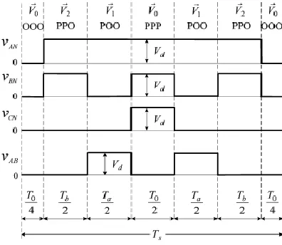
Figure 4 shows a seven-segment switching order and output of the inverter
Fig-4. Seven-segment switching order for Vref in sector I.
Available Online at www.ijpret.com 86
IV. Simplified space vector pwm method
For the three level inverter, three types of switching state-P, O and N in every phase, therefore there exist twenty-seven switching states within three-phase three-level inverter by using the three level inverter space-vector diagram, the basic principle of the explained SVPWM method could be perhaps easily achieved [6]. Switching states of every phase inverter are listed in table-2.
Table-2 Switching states and terminal voltages of the three level inverter.
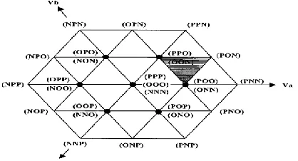
The space-vector diagram (SVD) of the three level inverter as shown in figure-5 which is made up of 6 small hexagons that are shown in the space-vector diagrams (SVD) of the conventional two-level inverters. Each of these six hexagons which constitutes the space-vector diagram (SVD) of the three level inverter, midpoints on the 6 high points of the inner small hexagons which is shown in the figure-6. Therefore by shifting these 6 small hexagons towards the center of inner hexagon by Vdc/3, the space-vector diagram (SVD) of the three level inverter has been simplified like a two-level inverter. To simplify the three level space-vector diagrams into the two-level space-vector diagram as explained above, the following two steps have to be taken.
1. Among the 6 hexagons one hexagon is selected within the position of the obtained
reference voltage [6].
2. Original reference voltage-vector (Vref) has to be deducted by measure from center voltage
vector about the specified hexagon [6].
By following the above two steps, the three level space-vector diagram is transformed to a two-level space-vector diagram. Then the switching order determination and the calculation of voltage vector duration time are done as the conventional SVPWM method of two-level. As the recommended SVPWM method is same in principle of conventional two-level SVPWM, various techniques used in two-level SVPWM can be applied to this proposed method too [6].
Switching Symbols Switching States Terminal Voltage
S1X S2X S3X S4X
Available Online at www.ijpret.com 87 Fig-5. Space-vector diagram of the three level inverter.
Source- [6].
Fig-6 Simplification of a three-level space-vector diagram. Source- [6].
V. Simulation Results
Simulation results have been taken for MODULATION INDEX ma=1,sampling timeTs = 1/Fs ,Fs is the sampling frequency that is taken to be 2.1khz and the input voltage (E) is applied to be 200volts for both two-level and three-level inverters.
(a)
(b)
Available Online at www.ijpret.com 88
VI. CONCLUSION
The SVM technique has been presented for two level inverter. Also, the proposed SVPWM method for the three level inverter has been described in detail. Calculation of dwelling times for voltage vectors have been conducted same as the two-level SVPWM. Thus the explained method minimizes the processing time of three-level SVPWM. This technique can be implemented to the multi-level SVPWM method above four-level. The effectiveness of the presented SVPWM method is demonstrated and verified by experimental results.
Acknowledgment
I would like to express my sincere gratitude to my project guide Prof. M. J. Katira (HOD) and research scholar Mr.Irfan Ahmed, from VNIT Nagpur for his valuable guidance. Lastly, I owe my deepest gratitude to my husband Mr. Prashant, my family and 18 months daughter Anvi who always stood behind me and showed their patience and support during this project.
REFERENCES
1. Wu, B.: ‘High-power converters and ac drives’ (IEEE Press,2006)
2. Irfan Ahmed, Vijay B. Borghate. ‘Simplified space vector modulation technique for
seven-level cascaded H-bridge inverter’, IET Power Electron., 2014, Vol. 7, Iss. 3, pp. 604–613, doi: 10..1049/iet-pel.2013.013
3. Nabae, A., Takahashi, I., Akagi, H.: ‘A new neutral-point clamped PWM inverter’, IEEE Trans.
Ind. Appl., 1981, IA-17, (5), pp. 518–523
4. Rodriguez, J., Lai, J., Peng, F.Z.: ‘Multilevel inverters: a survey of topologies, controls, and
applications’, IEEE Trans. Ind. Electron., 2002, 49, (4), pp. 724–738
5. Kouro, S., Malinowski, M., Gopakumar, K., et al.: ‘Recent advances and industrial applications
of multilevel converters’, IEEE Trans. Ind. Electron., 2010, 57, (8), pp. 2553–2580
6. Jae Hyeong Seo, ‘A new simplified space-vector PWM Method for three-level inverters’ in
IEEE Transactions on power electronics, Vol.16, No.4, July 2001.
7. Wei, S., Wu, B., Li, F., Liu, C.: ‘A general space vector PWM control algorithm for multilevel
inverters’. Proc. 18th Annual IEEE APEC, 2003, vol. 1, pp. 562–568
8. Zhang, H., Jouanne, A., Dai, S., Wallace, A.K., Wang, F.: ‘Multilevel inverter modulation
Available Online at www.ijpret.com 89
9. Celanovic, N., Boroyevich, D.: ‘A fast space vector modulation algorithm for multilevel
three-phase converters’, IEEE Trans. Ind. Appl., 2001, 37, (2), pp. 637–641
10.Massoud, A.M., Finney, S.J., Cruden, A., Williams, B.W.: ‘Mapped phase-shifted space vector
modulation for multi-level voltage-source inverters’, IET Electr. Power Appl., 2007, 1, (4), pp. 622–636
11.Massoud, A.M., Finney, S.J., Williams, B.W.: ‘Mapped hybrid spaced vector modulation for
multilevel cascaded-type voltage source inverters’, IET Power Electron., 2008, 1, (3), pp. 318– 335
12.Adam, G.P., Finney, S.J., Ojo, O.,Williams, B.W.: ‘Quasi-two-level and three-level operation
of a diode-clamped multilevel inverter using space vector modulation’, IET Power Electron., 2012, 5, (5), pp. 542- 551
13.Gopinath, A., Mohamed, A.S.A., Baiju, M.R.: ‘Fractal based space vector PWM for multilevel