Special Purpose
Special Purpose
Zener Diode
Zener Diode
The zener diode – silicon pn-junction
device-designed for operate in the reverse-biased
region.
The breakdown voltage of a zener diode is set
by carefully controlling the level during
manufacture.
The basic function of zener diode is to
maintain a specific voltage across it’s
terminals within given limits of line or load
change.
Typically it is used for providing a stable
reference voltage for use in power supplies
and other equipment.
If a zener diode is forward biased it operates
Zener Diode
Zener Diode
Zener Diode
Zener Diode
Zener Breakdown
Zener Breakdown
Zener diodes are designed to operate in reverse breakdown. Two
types of reverse breakdown in a zener diode are avalanche and zener. The avalanche break down occurs in both rectifier and zener diodes at a sufficiently high reverse voltage. Zener breakdown occurs in a
zener diode at low reverse voltages.
A zener diode is heavily doped to reduced the breakdown voltage. This causes a very thin depletion region. As a result, an intense electric field exists within the depletion region. Near the zener
breakdown voltage (Vz), the field is intense enough to pull electrons from their valence bands and create current. The zener diodes
breakdown characteristics are determined by the doping process. Low voltage zeners less than 5V operate in the zener breakdown range. Those designed to operate more than 5 V operate mostly in
Breakdown Characteristics
Breakdown Characteristics
The reverse voltage (VR) is increased – the reverse current (IR) remains extremely small up to the “knee”of the curve
Reverse current – the zener current, IZ
At the bottom of the knee- the zener breakdown voltage (VZ) remains constant although it increase slightly as the zener current, IZ increase.
IZK – min. current required to maintain voltage regulation
IZM – max. amount of current the diode can handle without being damage/destroyed
IZT – the current level at which the VZ rating of diode is measured
The zener diode maintains a constant voltage for value of reverse current rating from IZK to IZM
A zener diode operating in
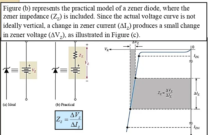
Zener Equivalent Circuit
Zener Equivalent Circuit
Z Z Z I V Z
[image:7.720.17.687.69.506.2]Ex 3-1
Ex 3-1 A zener diode exhibits a certain change in V
Zfor a certain
change in I
Zon a portion of
the linear characteristic curve between I
ZKand I
ZMas illustrated in Figure. What is the zener impedance?
Zener Power Dissipation
Zener Power Dissipation
Zener diodes are specified to operate at a
maximum power called the maximum dc
power dissipation, P
D(max).
Zener Diode Applications –
Zener Diode Applications –
Zener Limiting
Zener Limiting
Ex 3-8
Varactor Diodes
Varactor Diodes
Varactor Diodes
Varactor Diodes
Reverse bias voltage ↑ , depletion region ↑ , effectively the plate separation ↑ & the dielectric thickness ↑ , thus the
capacitance ↓ .
When the reverse bias voltage ↓ , the depletion region ↓ - the capacitance ↑
The capacitance is expressed by the following formula
; = plate area, = dielectric constant, = dielectric thickness
The capacitance parameters are controlled by the method of doping near the pn junction and the size and geometry of the diode’s construction.
LEDs
LEDs
When the devices is FB – e- cross the pn
junction from the n-type material &
recombine with holes in p-type material,
Recombining release energy in the form of
heat and light.
A large exposed surface area on one layer
of the semi-conductive material permits
the photons to be emitted as visible light –
electroluminescence.
Various impurities are added during the
LEDs
LEDs
LED Semiconductor Materials:
- GaAs, GaAsP, GaP
LED Biasing:
- The forward voltage across an LED is considerably greater than for a silicon diode
- The max. VF for LEDs is 1.2V – 3.2V
LED Applications
LED Applications
Used for indicator lamps & readout displays on a wide variety
of instruments, ranging from consumer appliances to
scientific apparatus.
Common type of display device using LEDs – 7-segment
display.
IR light-emitting diodes – used in optical coupling applications
– often in conjunction with fiber optics.
Area of application include – industrial processing & control,
Photodiode
Photodiode
Photodiode
Photodiode
An increase in the amount of light intensity – irradiance (mW/cm2), produces an
Current regulator diodes
Current regulator diodes
Current regulator diodes
keeps a constant
Schottky diode
Schottky diode
The
Schottky diode’s
significant characteristic is it’s
fast switching speed.
Pin Diode
Pin Diode
The Pin Diode is consists of heavily doped p & n regions separated
by an intrinsic (i) region
When reverse-biased – acts like constant capacitance.
When forward-biased – acts like a current controlled variable
resistance.
Low forward resistance of the intrinsic region decrease with
increasing current.
Used in mostly microwave frequency applications. Its variable
Laser Diode
Laser Diode
Laser - Light amplification by stimulated emission of radiation Laser light is monochromatic – consists of a single color – called
coherent light
Normally emits coherent light – consists of a wide band of
wavelength, whereas the LED emits incoherent light
A pn junction is formed by two layers of doped GaAs
The length of the pn junction bears a precise relationship with the
wavelength of the light to emitted.