University of New Orleans University of New Orleans
ScholarWorks@UNO
ScholarWorks@UNO
University of New Orleans Theses and
Dissertations Dissertations and Theses
12-15-2006
A Parallel Architecture for Analog-to-Digital Conversion with
A Parallel Architecture for Analog-to-Digital Conversion with
Improved Dynamic Range
Improved Dynamic Range
Brandy Sausse
University of New Orleans
Follow this and additional works at: https://scholarworks.uno.edu/td
Recommended Citation Recommended Citation
Sausse, Brandy, "A Parallel Architecture for Analog-to-Digital Conversion with Improved Dynamic Range" (2006). University of New Orleans Theses and Dissertations. 502.
https://scholarworks.uno.edu/td/502
This Thesis is protected by copyright and/or related rights. It has been brought to you by ScholarWorks@UNO with permission from the rights-holder(s). You are free to use this Thesis in any way that is permitted by the copyright and related rights legislation that applies to your use. For other uses you need to obtain permission from the rights-holder(s) directly, unless additional rights are indicated by a Creative Commons license in the record and/or on the work itself.
A Parallel Architecture for Analog-to-Digital Conversion with Improved Dynamic Range
A Thesis
Submitted to the Graduate Faculty of the
University of New Orleans
In partial fulfillment of the
Requirements for the degree of
Master of Science
in
Engineering
by
Brandy Sausse
B.S. University of New Orleans, 1998
Dedication
I am dedicating this work to my late mother. She was a pillar of strength even while she
was battling ovarian cancer. She always had a smile and never complained. I only hope that I
can become half the person that she was. I love you and miss you.
To my loving husband, I am so much more since you have come into my life. Thank you
for all of your support though this endeavor. I look forward to starting the next phase of our life
Acknowledgements
First I would like to thank Dr. Huimin Chen for taking me as his graduate student. You
were always more than willing to help me out even with your busy schedule. When I wanted to
change my topic after first struggling with my first topic choice, you cheerfully went along and
let me do my work. Thank you for steering my in the right direction when I was off-track and
creating a paper that I can be proud of. I know that it wasn’t easy since I was working full-time
and you were always willing to work around my schedule even if it meant working on the
weekends or late at night.
To my in-laws, I want to thank you for taking care of me while Bert was away. I
appreciate you fixing me dinner and keeping me company. Thank you for running the errands
when I didn’t have time to do them and for telling me that I could do this.
Dad, thank you for believing in me. You always knew that I could be anything that I
wanted. I know that you have not had an easy time lately, and I regret that my schoolwork kept
me away for being there for you as you had always been for me when I needed it.
Lastly, I would like to thank my loving husband, Bert. If it was not for you I would not
have even had the confidence in myself to go back to school. You knew that I was capable of so
much more. You had faith in me even when I didn’t have faith in myself. You had sacrificed so
much so I could have this opportunity. Thank you for supporting me, taking care of everything,
and letting me vent to you even if I did not show you my appreciation. Thank you for pushing
me through this even when I did not feel like working. I know that I would not have been able to
do this without your support. I know that with you I can achieve anything and I look forward to
Table of Contents
List of Figures ... vii
Abstract ... viii
Introduction... 1
Chapter 1 – Background ... 3
1.1 Motivation of This Work ... 3
1.2 Survey of Existing High-Speed COTS Components ... 6
1.3 Existing Techniques and Their Drawbacks ... 11
1.3.1 Stacked ADC ... 11
1.3.2 Time Interleaved ADCs ... 13
Chapter 2 - Design of the Parallel ADC System... 15
2.1 System Overview ... 15
2.2 System Components... 17
2.2.1 Signal Preprocessing ... 17
2.2.1.1 DC Block ... 17
2.2.1.2 DC Bias... 17
2.2.1.3 Clamping Diodes ... 18
2.2.1.4 AC Coupling ... 18
2.2.2 Analog to Digital Conversion ... 18
2.2.3 Digital Bias ... 18
2.2.4 Digital Summation ... 19
2.3 Performance Metrics ... 19
2.3.1 Sine Wave Reconstruction ... 20
2.3.2 Static Transfer Testing ... 22
2.3.3 Analog Power Test... 23
2.4 Analysis of Performance Improvement ... 23
2.4.1 Number of Bits of the Parallel ADC Architecture... 23
2.4.2 Dynamic Range of the Parallel ADC Architecture... 24
Chapter 3 - Design Example ... 25
3.1 Actual Design... 25
3.2 Design Summary... 28
3.3 Simulation Study... 28
3.3.1 ADC Model Description ... 28
3.3.2 Simulation Results of the Parallel ADC System... 29
3.3.2.1 Sine Wave Reconstruction... 32
3.3.2.2 Static Transfer Testing... 36
3.3.2.3 Analog Power Test... 39
3.3.3 Summary of Simulation Results ... 53
Chapter 4 - Conclusions and Future Work ... 54
4.1 Summary of Thesis ... 54
4.1.1 Findings... 55
4.1.2 Limitations ... 56
4.2 Future Work ... 56
Appendix... 58
List of Figures
Fig. 1. CWSF Block Diagram... 3
Fig. 2. Stated Number of Bits vs. Sampling Rate of COTS ADCs... 7
Fig. 3. ENOB vs. Sampling Rate of COTS ADCs... 8
Fig. 4. Performance Metric vs. Stated Number of Bits in COTS ADCs ... 10
Fig. 5. Performance Metric vs. Sample Rate in COTS ADCs ... 11
Fig. 6. Parallel system voltage divisions... 16
Fig. 7. System Block Diagram with n-Parallel ADCs ... 16
Fig. 8. Signal Preprocessing... 17
Fig. 9. Histogram of the Number of Converters ... 26
Fig. 10. Power Performance Metric for Remaining ADCs... 27
Fig. 11. Analog Devices ADCs Performance Metric ... 28
Fig. 12. Noise Floor, 210MHz fs... 31
Fig. 13. Noise Floor, 10MHz fs... 32
Fig. 14. Signal –0.5dBFS, 210MHz fs, 31.7038MHz fin... 33
Fig. 15. Signal –0.5dBFS, 210MHz fs, 103.0197MHz fin... 34
Fig. 16. Signal –0.5dBFS, parallel and single, 10MHz fs, 1.5097MHz fin... 35
Fig. 17. Signal –0.5dBFS, parallel and single, 10MHz fs, 4.9057MHz fin... 36
Fig. 18. Code Differences at 10MHz ... 37
Fig. 19. Code Differences at 100MHz ... 37
Fig. 20. Composite DC Static Transfer Curve... 38
Fig. 21. Averaged DC Static Transfer Curve... 38
Fig. 22. Amplitude Matching, 210MHz fs, 31.7038MHz fin... 40
Fig. 23. Amplitude Matching, 210MHz fs, 103.0197MHz fin... 41
Fig. 24. Amplitude Matching, 10MHz fs, 1.5097MHz fin... 42
Fig. 25. Amplitude Matching, 10MHz fs, 4.9057MHz fin... 43
Fig. 26. SFDR, 210MHz fs, 31.7038MHz fin... 44
Fig. 27. SFDR, 210MHz fs, 103.0197MHz fin... 45
Fig. 28. SFDR, 10MHz fs, 1.5097MHz fin... 46
Fig. 29. SFDR, 10MHz fs, 4.9057MHz fin... 46
Fig. 30. ENOB, 210MHz fs, 31.7038MHz fin... 48
Fig. 31. ENOB, 210MHz fs, 103.0197MHz fin... 49
Fig. 32. ENOB, 10MHz fs, 1.5097MHz fin... 50
Fig. 33. ENOB, 10MHz fs, 4.9057MHz fin... 51
Fig. 34. THD, 210MHz fs, 31.7038MHz fin... 52
Abstract
In this thesis, a parallel architecture for Analog-to-Digital Converters (ADCs) is
developed to increase the system dynamic range. The proposed architecture is a critical
component for a Continuous Wave Stepped Frequency (CWSF) radar system. Existing
Commercial Off-The-Shelf (COTS) components are inadequate to meet the demands of a high
sample rate and a high dynamic range specification. The proposed parallel architecture meets
the design criteria by extending the upper voltage limit of high sample rate converters. Extensive
Introduction
The main focus of this thesis is to determine if a parallel architecture of Analog to Digital
Converters (ADCs) can be used to obtain a better system dynamic range than that of a single
converter. This type of configuration is applicable to a Continuous Wave Stepped Frequency
(CWSF) radar system. Existing CWSF radar system has to use less power than those using a
pulsed frequency. This is due to the cross-coupling term from the transmitter to the receiver. As
a result, there is less power to be illuminated to the target. If the power that can be received is
increased, it will lead us to believe that extra power can be used to transmit to the target –
allowing targets with a smaller Radar Cross Section (RCS) to be seen.
Chapter 1 provides more details of the CWSF radar, the ADC survey, and several
techniques that have been developed over the years in order to increase either the dynamic range
of ADCs or their sampling rates. The stacked ADC approach is a multi-chip solution that has a
fixed gain state before each converter. The time-interleaved system is also a multi-converter
system. However, it increases the overall sampling rate by having the converters sample the
same signal at different points in time. Each individual converter cannot exceed its limit in the
sample rate.
The design of the parallel ADC system is closely examined in Chapter 2. The objective
is to increase the dynamic range of the system so that the transmit power of a CWSF radar can be
increased. By assigning each individual converter a particular voltage range to digitize, the
incoming signal will then have the amplitude n times greater than that of the individual
converter.
A design example is provided in Chapter 3 illustrating the design considerations for part
an overall dynamic range of 80dB. Several manufacturers’ components were examined and
analyzed. Performance metrics are used to make the final component selection. A practical
system analysis is performed to determine the overall system performance against several
metrics. Extensive simulation study has also been performed to determine the dynamic
performance. Although the system has an increase to the voltage amplitudes that can be input
into the system, several other related issues have been examined and further simulation study has
been suggested.
Conclusions are presented in Chapter 4. This includes the findings from the theoretical
analysis and simulation as well as some known limitations of the parallel architecture for the
Chapter 1 – Background
1.1 Motivation of This Work
In order for a radar system to detect a target, an electromagnetic wave is transmitted into
the air. If a target is located in this transmit path, then part of the signal can be reflected back to
the radar receiver. The amount of energy that is reflected back depends partially on the target’s
Radar Cross-Section (RCS). A basic block diagram of a Continuous Wave Stepped Frequency
(CWSF) radar system can be seen in Fig. 1 [1], [2] and will be described in detail below.
Target Clock
DDS Upconverter Power Amp Tx Antenna
Low Noise Amp Rx Antenna
ADC Control
Fig. 1. CWSF Block Diagram
A CWSF radar differs from a traditional radar in two ways. First, it sends out a set of
discrete frequencies instead of one pulse that has a continuous frequency sweep [3]. Second, it
continuously sends out this signal – necessitating a need for two separate antennas.
The sets of discrete frequencies that are spaced equally apart are usually generated by the
Direct Digital Synthesizer (DDS) component. The DDS acts as a function generator by using
Converter (DAC) [4]. These frequencies are then upconverted and transmitted out of the
transmit antenna. Typically, an ultra wideband Archimedean spiral antenna is used in these
systems [5]. A target will reflect a portion of this signal back to the receive antenna. The
amount of reflection is determined in part by the target’s Radar Cross Section (RCS) as well as
by the power transmitted by the radar system. The energy of the signal that is received at the
radar is expressed in equation (1) [6]. In this equation, “Pr is the received peak power (W), Pt is
the transmitted peak power (W), Gtis the gain of the transmitter antenna (ratio, not dBi), Gr is
the gain of the receiver antenna, σ is the radar cross-section of target (RCS), c is the speed of
light, f is the transmitted frequency , RTx is the transmitter range to target , and RRx is the receiver
range from target.”
( )
f R R[
dBWc G G P P Rx Tx r t t r ⎥ ⎥ ⎦ ⎤ ⎢ ⎢ ⎣ ⎡ ⎟⎟ ⎠ ⎞ ⎜⎜ ⎝ ⎛ = 2 2 2 3 2 10 4 log 10 π σ
]
(1)The received signal is down converted into a signal that can be processed by an
analog-to-digital converter. After the signal is digitized, advanced digital signal processing techniques
can be performed – such as applying a window function to shape the power spectral density to
attenuate the sidelobe effect [5].
The performance of the CWSF radar is determined from the unambiguous range and the
range resolution [5]. The unambiguous range (Run) is calculated from the propagation velocity (v
= 3×10⁸m/s) and the frequency step (Δf) as shown in (2). From this equation, we can see that the
smaller the frequency step, the greater the unambiguous range of the system.
f v Run
Δ =
The bandwidth (B) of the system (defined as fmax – fmin) plays a crucial role in the range
resolution (Δr). Equation (3) shows the importance of this specification. It is shown that an
increase in bandwidth of the system will give a smaller range resolution. To reduce the number
of downconverters that are needed, the analog-to-digital converter needs to be able to
accommodate the high-sampling rates that are required from the large bandwidths.
B v r
2 =
Δ (3)
However, as stated by Pieraccini [7], the receiver in a continuous wave radar can be
blinded by the direct transmit power. This stems from the fact that the transmit and receive
antennas are closely located so that there are no periods where the system is not transmitting –
resulting in a cross-coupling signal. One possible way to reduce this effect is to have the receive
Archimedean spiral antenna with an opposite rotation of that of the transmit antenna [5].
However, the resulting system will still have the cross-coupling signal present and will typically
have to use less transmit power than that of a conventional pulsed radar. By referring back to
(1), with the reduced transmitted energy we can see that the signal received at the radar will be
reduced. Since the transmit power is limited, the size of the RCS that can be seen by the system
is reduced. If the input voltage of the analog-to-digital converter is increased, the power at the
radar receiver will also be increased provided that the downconverters before the ADC are
chosen to accommodate these increased power levels. With the increase in receiver power
capability, the transmit power will then be increased because the receiver is able to handle the
higher cross-coupled signal. Taking the ratio of the newly received power to the old one, the
new RCS can be calculated. The derivation is provided in the Appendix. The minimum size of
(
)
[
]
[
( )
]
( )
3 2 2 2 2 10 10 4 , log log , 10 Rx Tx r t tNew rOld Old r t tOld rNew B New R R f c A A G G P P A G G P P B π = − σ = =σ (4)
1.2 Survey of Existing High-Speed COTS Components
There are several types of analog to digital converters being used in the existing radar
systems [8]. The ΣΔ converters are typically lower speed and higher resolution converters
because they use an oversampling technique to shape the noise floor. Higher speed converters
typically use either a successive approximation (SAR) or a pipeline – or flash – architecture.
The SAR architecture utilizes a sample-and-hold scheme. The output of the sample-and-hold is
then fed into a comparator, which compares the input signal with a signal from a DAC that is
controlled by a successive approximation register. The accuracy of this converter is limited by
the internal DAC. It is a serial output device that has no “pipeline” delay.
The flash architecture utilizes a sub-ranging technique that employs a bank of parallel
comparators with different voltage references determined by a resistor divider network. It does
not require a sample-and-hold step. These chips are generally used for applications with 1Gsps
or higher because they are high-powered GaAs devices.
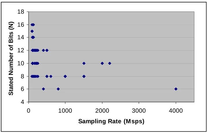
An ADC survey of components with 100Msps sampling rate or higher was performed to
determine what was the latest in high-speed converters on the market today – see Table 1 in the
Appendix for component specifications. Fig. 2 shows the sampling rate of the COTS ADCs vs.
the stated number of bits of components from several manufacturers. These included Analog
Devices [9], Atmel [10], Datel [11], Linear Technology [12], Maxim [13], National
Semiconductor [14], and Rockwell Scientific [15]. From this plot, we can conclude that higher
4 6 8 10 12 14 16 18
0 1000 2000 3000 4000
Sampling Rate (Msps)
Stated N
u
mber of B
its (N
)
Fig. 2. Stated Number of Bits vs. Sampling Rate of COTS ADCs
The performance of ADCs is best indicated when the effects of distortion are taken into
account. The Effective Number Of Bits (ENOB) is used as an indicator of how well the
converter digitizes without distortion due to the sample-and-hold operation [16]. Fig. 3 shows
how the actual performance of the converters differs from the stated number of bits. We can see
that converters with the same stated number of bits on the datasheet have a variance in their
performance. As the sample rate of the converter increases, the ENOB of these converters
4 6 8 10 12 14 16 18
0 1000 2000 3000 4000
Sampling Rate (Msps)
ENOB (b)
6-bit 8-bit 10-bit 12-bit 14-bit 15-bit 16-bit
Fig. 3. ENOB vs. Sampling Rate of COTS ADCs
Another useful metric first proposed by Walden in his 1999 ADC survey [17] and then
again in Le, Rondeau, Reed, and Bostian’s survey [16] can be used to compare the different
ADCs as shown in equations (7) and (8) In [16], several important performance metrics have
been discussed. Two of them are of particular importance to the design of the parallel ADC
system in this thesis. The first uses the Effective Number of Bits (ENOB) to determine how well
the system converts the analog signal into a digital one without introducing distortion. The
theoretical signal-to-noise ratio (SNR) is calculated from the number of bits in the converter as
shown in equation (5) [8] where N is the number of bits used in the ADC.
dB N
SNR=6.02 −1.76 (5)
However, with the distortion that is introduced by the ADC, we can derive an equation
similar to (5) to calculate the ENOB using the signal-to-noise-and-distortion ratio (SINAD). The
dB dB SINAD
ENOB
02 . 6
76 . 1 −
= (6)
The performance metric then can be calculated from the ENOB and the sampling rate of
the converter (fs) as seen in (7) [16]. The importance of the ENOB of the converter is weighted
more heavily in (7) than that of the sample rate. An increase in P indicates a better performing
converter.
(7)
s B
f P=2 ⋅
The second metric that was proposed in [16] was used in order to determine the power
efficiency of the converter. It takes the P metric from above and divides it by the amount of
power that the chip uses. This will give an idea of how much power (Pdiss) is needed for a certain
resolution and sampling rate. The formula is shown in equation (8). As evidenced by this
equation, the lower the amount of power that a converter uses will translate to an increase in F
because it is more efficient than a converter that has the same ENOB and sampling rate.
diss s B
P f
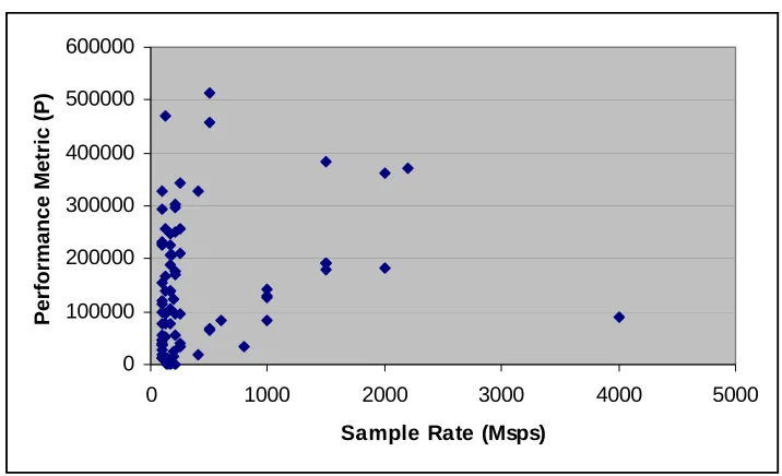
The performance metrics (P) of the sampling rate and ENOB of the COTS ADCs are
shown in Fig. 4. It is plotted against the stated number of bits (N) from each component’s
datasheet. As can be seen in this figure, the ADC with the highest performance metric is a 12-bit
converter [9]-[15].
0 100000 200000 300000 400000 500000 600000
0 5 10 15 20
Stated Number of Bits (N)
Performance Metric (P)
The performance metric is then plotted against the sample rate in Fig. 5. The converter
that has the highest performance metric in this plot is one with a sample rate of 500Msps.
0 100000 200000 300000 400000 500000 600000
0 1000 2000 3000 4000 5000
Sample Rate (Msps)
Performance Metric (P)
Fig. 5. Performance Metric vs. Sample Rate in COTS ADCs
1.3 Existing Techniques and Their Drawbacks
Techniques have been devised and studied to increase the performance of COTS ADCs
in systems. These consist of two main methods – increase the dynamic range of high-speed
converters, or increase the sample rate of high-dynamic range converters. Both of these will
increase the performance metric P. However, the increase in P comes at a cost of increased
power, which could potentially cause F to decrease. Two examples of these methods will be
discussed in detail in the following sections.
1.3.1 Stacked ADC
The stacked Analog-to-Digital Converter concept was first introduced by V.
Hansen, S.M Brockett, and P. Cahill [18]. It was then refined by S. R. Duncan, V.
ADCs that are available do not posses the dynamic range that is required for modern radar
systems. A dynamic range of 80 to 100 dB of dynamic range is required to detect the smallest
signals of the target return, yet still operate linearly in the presence of a large signal return.
Traditional techniques such as sensitivity time control (STC), automatic gain control (AGC), and
bandpass intermediate frequency (IF) limiting all have undesirable effects in a radar system, such
as short-range detection degradation and pulse compression sidelobe degradation, transients that
can trigger false alarms, and nonlinearities. The stacked ADC approach was proposed to
eliminate these effects while improving the dynamic range of the system as will be explained
next.
To test the response of the stacked ADC approach, test circuits were designed and
prototyped. The configuration consists of parallel ADC that each has an individual gain step
before the conversion stage. Each gain step is spaced ΔdB apart from the previous stage, for a
total system gain of (n-1)Δ dB over a single ADC, where n is the number of converters in the
stacked system. To determine which converter would be used for the signal, a receive level
indicator is placed before any of the gain stages. Also, the indicator serves a purpose to switch
off inputs to the gain stages so damaging signals would not be seen by the gain components and
so noise would not be introduced into the system. Once this system was tested, the results were
shown to improve upon the current single ADC by approximately 30dB.
The only limitation is that this configuration would not improve the signal-to-noise ratio
(SNR) or the spurious response of any individual ADC component. This system could not be
used in the CWSF radar system due mainly to the cross-coupling signal. This signal has the
largest amplitude and is always present. As such, the stacked ADC system would trigger off of
1.3.2 Time Interleaved ADCs
Another approach that has been researched to improve the performance of ADCs is to
have multiple ADCs that are time interleaved. This will increase the effective sample rate of a
system to nfs where n is the number of ADCs used and fsis the sample rate of one converter.
This will enable having higher resolution at a faster sampling rate because often the slower
ADCs have a higher resolution, thus achieving a similar effect as previously discussed by using a
different approach. However, due to manufacturing variations between components such as
gain, offset, and timing mismatches, the spurious free dynamic range (SFDR)/ signal to noise
and distortion ratio (SINAD) will be decreased. This topic has been studied in several IEEE
journal articles briefly summarized as follows.
C. Vogel’s article [20] dealt with studying the effects of these mismatches on the SINAD
and calculating the explicit effects each of these individual components directly has upon the
SINAD ratio. The equations were derived and a statistical analysis was performed. The
interaction of these effects was also studied to determine where designers of time-interleaved
systems should focus their efforts to minimize these mismatches. Techniques to mitigate these
effects were not covered in this research.
N. Vun and A. B. Premkumar [21] proposed a mitigation technique using a polyphase
decimation filter. It was proposed to perform both the multirate processing that is required for
software defined radios (SDRs) and to reduce the effects of the mismatch errors. The theory is
that the mismatch would be reduced because of the interleaving process of the polyphase filter.
However, research was not proven in the framework of the article.
J. Elbornsson, F. Gustafsson, and J. E. Elkund’s [22] article presented a randomly
rate, but having ΔM extra converters would enable converters to be chosen at random as long as
the individual ADC sampling rates would not be exceeded. A probabilistic analysis was
performed on the randomly interleaved system and was shown to reduce the distortion to
noise-like levels. In this article linearity errors were not studied.
Although this technique has much research put forth, it cannot be directly applied to the
CWSF radar system. This method utilizes slower converters that have a higher resolution.
However, the resolution converters that are needed to meet the dynamic range requirements of
the radar system require too many converters to be practical. For example, if we choose the
fastest 24-bit converter made by Analog Devices, i.e., the AD7760 that had a throughput rate of
Chapter 2 - Design of the Parallel ADC System
2.1 System Overview
The purpose of the design of an ADC system with improved dynamic range is to increase
the performance of the CWSF radar. When a higher output signal can be transmitted from the
radar, then smaller targets can be illuminated. However, with the increase in transmit power,
there will be an increase in the received signal from the cross coupling. To accommodate this
undesirable effect, the parallel ADC configuration is a natural candidate that can increase the
amplitude of the signal being received by the system.
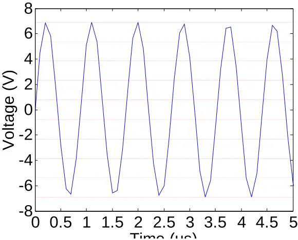
The parallel architecture of this system is designed so that separate converters will
process the incoming signal simultaneously in order to preserve the ADC sampling rate. Each
ADC converter will have a separate designated voltage range of the incoming signal that it will
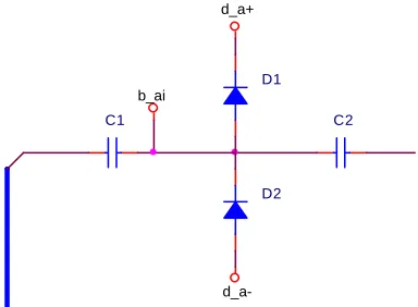
process as shown in Fig. 6. For this representation, the signal will be processed by nine ADCs.
The original signal is the blue waveform whereas the red lines show the voltage limits for each
ADC. For instance, ADC 1 will process the signal from 6.912V to 5.376V. Fig. 7 shows the
top-level block diagram of this system. After the signal pre-processing block, only the voltage
level assigned to the ADC will be available, shifted to the input voltage range of the individual
converter. The signal pre-processing block can be seen as in Fig. 8. Next, the digital signal will
have to be processed to convert it into the correct output code for the parallel system. This step
is achieved though the digital bias. Afterwards, the signals are summed together to form the
finial digital signal. The whole processing scheme and system components will be discussed in
0 0.5 1 1.5 2 2.5 3 3.5 4 4.5 5
-8
-6
-4
-2
0
2
4
6
8
Time (us)
Volt
age (V)
Fig. 6. Parallel system voltage divisions
Fig. 7. System Block Diagram with n-Parallel ADCs Signal
Pre-processing 1
Signal
Pre-processing n
.
.
ADC 1
ADC n
.
.
Digital Bias
1
Digital Bias
n
.
.
Digital
Summation
Input
C1
D1
D2 C2
b_ai
d_a+
d_a-Fig. 8. Signal Preprocessing
2.2 System Components
2.2.1 Signal Preprocessing
2.2.1.1 DC Block
The purpose of this component is to block the DC bias that will be added in the next
processing step.
2.2.1.2 DC Bias
The DC biasing step is used to set the voltage range of the signal that will be digitized by
the ADC. Equation (9) is used to calculate the voltage level needed for each segment, where bai
is the analog bias level at the ith converter, s is the input span of the individual converter, and n is
the number of converters.
( )
( )
[
i s]
bb
s sn b
ai 1
2 2
0 0
− + =
⎥⎦ ⎤ ⎢⎣ ⎡ + − =
The positive segments of the signal will need to be biased negatively to shift the top part of the
signal to the range of the ADC. The opposite is needed for the negative segments of the signal.
Each DC bias can be generated by a precision voltage reference.
2.2.1.3 Clamping Diodes
In order to keep the ADC from saturating, clamping diodes will be used. Any part of the
signal that lies outside of the voltage range of the ADC will be held to the voltages connected to
the diodes. The voltage references for each diode will be determined by equation (10), where da+
is the positive diode rail, da- is the negative diode rail, and vd is the voltage drop across the diode.
d ai
a v
s b
d + = + +
2 a ai vd
s b d − = − −
2 (10)
2.2.1.4 AC Coupling
The last step before the digitization involves ac-coupling the signal into the ADC via a
capacitor. This step is necessary to bring the signal back into the input range of the ADC.
Instead of having the signal biased around the DC bias voltage, it will bias back to 0V and the
portion of the signal of interest will be able to be digitized.
2.2.2 Analog to Digital Conversion
Each signal piece is then converted by their individual ADCs. The output of the
converters will all have the same span of output codes.
2.2.3 Digital Bias
To get the digital signal back to its correct level, a digital bias has to be added in the same
how these bias levels are calculated. This assures that the each digital signal will be converted to
its correct quantization level.
( )
[
]
⎟⎟ ⎠ ⎞ ⎜⎜ ⎝ ⎛ − − − = ⎥ ⎦ ⎤ ⎢ ⎣ ⎡ ⎟⎟ ⎠ ⎞ ⎜⎜ ⎝ ⎛ − − ⎟⎟ ⎠ ⎞ ⎜⎜ ⎝ ⎛ − = 1 2 2 1 1 2 2 2 1 1 2 2 2 1 0 0 N a N N i d d n d (11)2.2.4 Digital Summation
The final step in the processing is to take all the digital outputs and sum them together.
This will result in a digital signal that is representative of the original analog signal. The number
of codes in the system is calculated using equation (12).
(12)
N
n C|| = 2
2.3 Performance Metrics
In order to evaluate the performance of the parallel ADC system, tests that are typically
used to evaluate the performance of ADC converters were performed [24]. Before the system
specifications are determined, a test of the basic functionality needed to be executed. After the
model of the system is validated, the static transfer code of the system is calculated. Estimates of
static gain errors, offset errors, missing codes, and code width errors can be determined by this
test. These errors can impact the radar system by creating uncertainty of the target locations.
Differences between the amplitude matching from the ideal digital signal to the signal output by
the system can also be translated to target location uncertainties.
The next several metrics are used to determine the range of radar returns that can be
return to be processed in the presence of a large return. The first metric is spurious free dynamic
range (SFDR). If a high SFDR is achieved, then smaller returns can be distinguished from the
noise floor. However, if there is a great amount of distortion that is present, then the smaller
returns will be lost – decreasing the range of target returns that can be processed. The range of
targets that can be processed by the system can also be determined by the ENOB since this is
calculated using the signal to noise and distortion ratio. Finally, the total harmonic distortion
(THD) is determined. A simulation study using MATLAB has been performed for the designed
ADC system – as explained in Section 0 – using the performance metrics below. However, the
main performance constraint in this system will be the amount of power required to operate.
This will be considered in the design of the system.
2.3.1 Sine Wave Reconstruction
The first step was to determine if a sine wave could be digitized properly. It is used to
test the basic functionality of the simulation. A sine wave at –0.5dB below the full-scale parallel
system range was input into the simulation and the resulting digital output was plotted to verify
correctness of the simulation. In addition, the ratio of the parallel system output level to the
single converter output level was taken to determine if the expected output increase was
achieved.
Several steps had to be taken to assure that the input signal would give data that would be
easier to process. First, if a sine wave was a direct multiple of the sample rate (fs), then the
sample values in the output of the FFT could become very repetitive and could potentially mask
any problems [25]. To assure that this would not occur, (13) was used to obtain a signal
(
)
1 . 0 5 . 26 ) ( 1 . 0 5 . 26 + = − = m round f f f f n s i s u (13)Once the input frequency was determined, the frequency bin width of the FFT could be
calculated. This was used to determine which FFT bin the input frequency would be located. To
assure that distinct phases were sampled by the FFT, an odd numbered bin was used for the
signal location [24]. For example, if an input signal of 71.3208MHz was being sampled by a
210MHz signal, and the FFT size is 32,768 samples, the frequency bin spacing would be
6.4087kHz. The fundamental frequency would be in bin number 11,129. If this number had
been even when calculated, the next bin would be used. The input signal is then recalculated
again to be the FFT bin number of the fundamental frequency multiplied by the FFT frequency
bin spacing.
To assure that all of the energy from the fundamental signal was located into one FFT
bin, the sampling had to be coherent [26]. Coherency is a way to ensure that the FFT (N) takes
an integer number of samples of the input signal (fi). To calculate how many periods (m) need to
be taken, (14) was used. Basically, we can view this as a conversion factor going from the FFT
samples into the time domain samples.
s i f N f
m= (14)
Next, the input signal step size and duration were calculated. The step size is just the
reciprocal of the sampling rate and the duration is the number of cycles that was calculated above
divided by the sampling rate. The final step in creating the analog signal has to do with the
ADIsimADCTM simulator – explained in Section 3.3.1 – for the analog-to-digital conversion.
data appears at the output of the ADC. Also, data is available for this same period of time after
the conversion period ends. To accommodate this step in the ADC conversion, zeros are
appended onto the input signal equal to the latency time.
After the signal was outputted by the system, the FFT of the data could be taken.
Because of the latency issue mentioned in the above paragraph, the FFT had to be taken starting
at the sample after the last one that corresponded to the latency period. In order to obtain the
frequencies for the x-axis of the FFT plot, zero to half of the FFT size was multiplied by the
conversion factor – sample frequency divided by the FFT size.
2.3.2 Static Transfer Testing
In this test, the output codes are plotted against the input voltages. This is used to
determine the linearity of the ADC system. Ideally, the voltage span of one Least Significant Bit
(LSB) would only map to one output code. However, this is not always true and the code width
– the minimum input voltage for a particular ADC output code – can vary due to processing and
manufacturing defects. To test the code width, eight individual voltages are tested for each
output code. IEEE standard 1241 ADC set this method forth for static transfer testing. This
allows an accurate measurement of the individual code width. To calculate the size of the
voltage steps, we use equation (15), with vs as the voltage step, s|| as the voltage span of the
parallel system, and N as the number of bits in an individual converter. This test was performed
at sample rates from 100 Hz to 100MHz to determine how the output was impacted.
N s
s v
2 8
|| ×
2.3.3 Analog Power Test
The purpose of this test is to determine how closely the output signal matches the
ideal digital signal, the Spurious Free Dynamic Range (SFDR), and the Effective Number Of
Bits (ENOB) of the system. The input amplitude is swept from the minimum voltage level to
0.5dB below full-scale in 50 steps. After the digital signals were obtained, the Fast Fourier
Transform (FFT) was performed to determine the SFDR – the difference between the maximum
signal and the next highest spurious tone in the noise floor. To calculate the ENOB, the
signal-to-noise-and-distortion Ratio (SINAD) is taken of the digital signals. The SINAD is the ratio of
the rms fundamental frequency to all of the noise including the harmonics. This is then put into
(6) [8]. The distortion that is caused by the converter decreases the dynamic range that is
available, resulting is a loss of the number of bits. These signals are plotted against the analog
input power in dBm to determine the change of SFDR and ENOB.
2.4 Analysis of Performance Improvement
2.4.1 Number of Bits of the Parallel ADC Architecture
The number of output codes of an ADC is defined by equation (16), where C is
the number of output codes and N is the number of bits in the ADC.
(16)
N
C =2
In the parallel ADC system, the number of output codes is just the number of codes of the single
ADC multiplied by the number of ADCs in the parallel system as shown in (17). C|| is the
number of different codes in the parallel system and n is the number of ADCs in parallel.
(17)
N
Using (16) and (17), we can calculate the number of bits (N||) that is represented by the parallel
system.
(
N)
n
N|| =log2 ×2 (18)
2.4.2 Dynamic Range of the Parallel ADC Architecture
The dynamic range of a system is an indication of the difference between the smallest
and largest signals that can be detected by the system as shown in equation (19), where dr is the
dynamic range of the ADC, s is the input range of the converter, and e is the minimum signal
that can be digitized by the ADC.
⎟ ⎠ ⎞ ⎜ ⎝ ⎛ =
e s
dr 20log10 (19)
Because the individual ADC has not changed in the parallel system, the minimum
detectable signal is the same as for the single ADC. The number of ADCs that are needed to
reach a specific dynamic range for the system can be determined from equation (20). Since there
can only be an integer number of converters in the parallel system and to assure that the dynamic
range requirements are met, the result will need to be rounded up.
⎥ ⎥ ⎥ ⎤ ⎢
⎢ ⎢ ⎡
= ⎟⎟⎠
⎞ ⎜⎜ ⎝ ⎛ −
20 20
||
10
dr dr
n (20)
This system still needs to be simulated in order to determine the dynamic performance
Chapter 3 - Design Example
3.1 Actual Design
For this design, we are going to perform an analysis on the converters surveyed in
Chapter 1 to determine which ones might provide a reasonable solution to obtain an 80dB system
dynamic range. This would result in a minimum 5dB increase in the maximum dynamic range
of the system from the surveyed ADCs [9] – [15]. This range was chosen because the clutter to
noise ratio (CNR) in radar systems can exceed 80 – 100dB [19]. Also, the higher dynamic range
allows a larger range of radar returns that can be processed – allowing a small return to be seen
simultaneously as a large return. For the first stage of the design, the sampling rate will not have
any bearing. This specification will follow later on in the design. An analysis was performed to
determine how many of each converter would be needed to obtain a system dynamic range (dr||)
of 80dB. To calculate this, we need to first look at the specified dynamic range for each
converter (SNR) and the input voltage span. Equation (17) was used with the specifications from
the datasheet of each individual converter and placed in a spreadsheet in order to determine how
many ADCs would be required. A spreadsheet was generated to keep track of all of the
components being surveyed along with their specifications. A histogram plot was created as
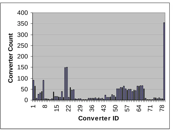
shown in Fig. 9 to determine what components would have a reasonable part count for the
system [9] – [15]. For the design example, only ADCs that require 10 or fewer in the parallel
0 50 100 150 200 250 300 350 400
1 8
15 22 29 36 43 50 57 64 71 78
Converter ID
Converter Count
Fig. 9. Histogram of the Number of Converters
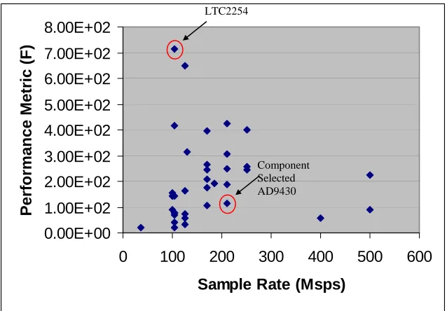
These remaining converters were then examined by using the performance metric F as
specified in (8). An assumption was made that the ENOB would be calculated in a similar
manner to (18) except that instead of having the number of bits of the converter (N), the ENOB
(B) of the individual converter would be used. The power dissipation was assumed to be just the
number of converters in the system (n) multiplied by the power dissipation of the individual
converter. In the actual system, the power dissipation will be higher than this number because of
the supporting components that are required. However, this approximation will be suitable to
determine the performance metric of the proposed system in order to best choose an ADC for the
design. The ADC power metric was then plotted as shown in Fig. 10. The component with the
highest performance metric was the Linear Technologies LTC2254, 14-bit 105Msps converter.
However, to quickly determine the system performance a simulation study was performed based
on a free software-modeling tool provided by Analog Devices. This approach could also allow
0.00E+00 1.00E+02 2.00E+02 3.00E+02 4.00E+02 5.00E+02 6.00E+02 7.00E+02 8.00E+02
0 100 200 300 400 500 600
Sample Rate (Msps)
Performance Metric (F)
LTC2254
Component Selected AD9430
Fig. 10. Power Performance Metric for Remaining ADCs
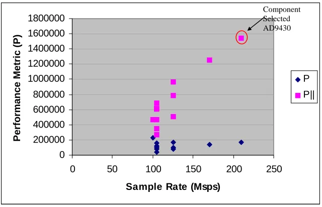
The performance metric (P) is plotted in Fig. 11 for only the Analog Devices components
in the single and parallel configurations. The Analog Devices AD9430, 12-bit 210Msps was
chosen for the parallel system. It requires nine converters to achieve an 80dB dynamic range
with an approximate power requirement of 13.5W for the converters. The estimate of the ENOB
used for the performance metric was 12.84 bits. The number of bits in the parallel system is
0 200000 400000 600000 800000 1000000 1200000 1400000 1600000 1800000
0 50 100 150 200 250
Sample Rate (Msps)
Pe
rfo
rma
n
c
e
Me
tric
(P)
P P||
Component Selected AD9430
Fig. 11. Analog Devices ADCs Performance Metric
3.2 Design Summary
The system was designed to have the following specifications:
• Dynamic range: 80dB
• ADC: AD-9430
• Max sample rate: 210Msps
• Minimum power: 13.5W
• ENOB: 12.84
3.3 Simulation Study
3.3.1 ADC Model Description
The ADC model used in this thesis is a MATLAB tool that is provided free of charge from
Analog Devices website (http://www.analog.com) called ADIsimADCTM [27]. It consists of
is output=mxadimodel(input, encoderate, freq, jitter, 0, key) or output=mxadimodel(input,
encoderate, 0, jitter, Nyquist, key). It requires the input signal that represents the analog voltage
to be converted. The encode rate is the sampling rate of the converter in Hertz. The freq is the
analog frequency in Hertz, however, this input can be determined from the Nyquist parameter.
The jitter allows the user to change the clock jitter going into the model. As mentioned above, if
the analog frequency is not known, then the required Nyquist frequency can be input. The key is
obtained from key=mxadimodel(‘input model file’).
These tools were designed by Analog Devices to provide engineers with a quick and simple
way to evaluate converters to determine if the performance of the ADC will be suitable for their
designs. These models are not bit-exact models. Bit-exact models will have a known response
to any analog input. However, this is not the case in real systems. Variations from component to
component, noise, and distortion are all part of systems. The models that were developed were
meant to be able to more accurately determine the dynamic performance of each individual
converter before building the hardware. The model takes into account the effects of offset, gain,
sample rate, bandwidth, jitter, latency, and both ac and dc characteristics.
3.3.2 Simulation Results of the Parallel ADC System
The simulations below were performed with the parallel ADC system to have a dynamic
range of 80dB. This was accomplished using nine Analog Devices AD9430 12-bit 210Msps
converters. This allowed for maximum voltage amplitude of 6.9120Vpp for the system. When
comparisons were made against the single converter configuration, the same sample rate and
input frequencies were used. The single converter configuration has a maximum voltage
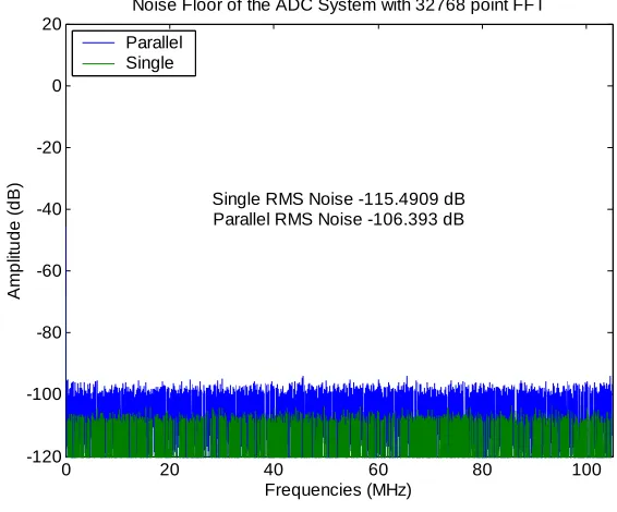
The noise floor of the system was compared to that of the single system. A signal of all
zeros was input into the system to determine the noise floor. After the signal was digitized, the
32k FFT was taken, and then normalized to the digital full-scale signal of a single converter.
Taking a signal with the maximum amplitude of a single converter and multiplying it by a
conversion factor (c) mentioned in (21) gives the ideal digital full-scale signal, which then needs
to be converted to the frequency domain (in dB). N is the number of bits and AM is the
maximum signal amplitude (Vp) of a single converter.
⎟⎟ ⎠ ⎞ ⎜⎜ ⎝ ⎛ =
M N
A
c 2 (21)
The FFT signal acts as a narrowband spectrum and will introduce a processing gain
dependant on the FFT size (M) as shown in (22) that will lower the noise floor [8]. The single
system will have a noise floor of approximately –116dB after taking into consideration the
processing gain of the FFT signal. The parallel system should have the same noise floor of the
single ADC system since the properties of the individual converters are not changed – only the
maximum signal amplitude that can be processed has changed.
⎟ ⎠ ⎞ ⎜ ⎝ ⎛ =
2 log
10 10
M
0 20 40 60 80 100 -120
-100 -80 -60 -40 -20 0 20
Noise Floor of the ADC System with 32768 point FFT
Frequencies (MHz)
A
m
pl
it
ud
e (
dB
)
Single RMS Noise -115.4909 dB Parallel RMS Noise -106.393 dB Parallel
Single
Fig. 12. Noise Floor, 210MHz fs
The noise floor of the parallel system is approximately 9dB higher than that of the single
converter configuration. This is likely due to the manufacturing variations of the separate
converters and the digital biasing performed.
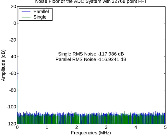
The noise floor was then calculated for a sampling rate that was equal to the minimum
sample rate of the converter (10MHz) to see the effects of the lower sampling rate. The noise
floor should be the same as the previous results. As shown in Fig. 13, the noise floor for the
single converter is 2.5dB below that of the maximum sample rate. In addition, the noise floor of
the parallel system is only 1dB higher than the single converter. This increase in performance is
0 1 2 3 4 5 -120
-100 -80 -60 -40 -20 0 20
Noise Floor of the ADC System with 32768 point FFT
Frequencies (MHz)
A
m
pl
it
ud
e (
dB
)
Single RMS Noise -117.986 dB Parallel RMS Noise -116.9241 dB Parallel
Single
Fig. 13. Noise Floor, 10MHz fs
3.3.2.1 Sine Wave Reconstruction
With this test, a sine wave was input into the system to validate the functionality of the
model and the system design. The input sine wave with a frequency of 31.7038MHz that was
0.5dB below full-scale was input into the system that had a sampling rate of 210MHz. The FFT
of the resulting digital signal was taken and normalized to the maximum digital signal of a single
converter. This was done to be able to compare the performance of the two systems. Since the
output amplitude of the system (A||) is nine times the single converter input amplitude level (As),
the expected output level (ΔA) of the parallel system will be approximately 19dB higher than that
of the single converter using equation (23). This performance that was expected was obtained as
shown in Fig. 14.
[ ]
⎟⎟⎠ ⎞ ⎜⎜ ⎝ ⎛ =
Δ
s
A A dB
0 20 40 60 80 100 -120
-100 -80 -60 -40 -20 0 20
FFT Plot of Signal -0.5dBFS
Frequency (MHz)
Am
pl
it
ud
e
(
d
B
)
← Frequency 31.7038 MHz
← Single Amplitude -6.9112 dB
← Parallel Amplitude 12.1826 dB
Fig. 14. Signal –0.5dBFS, 210MHz fs, 31.7038MHz fin
As is noticed in the graph, the parallel system appears to have more distortion present
than the single converter. This conclusion will be examined later when determining the
Effective Number of Bits.
The output signal near the Nyquist rate should remain the same as that from the lower
input frequency because the AD9430 has a 700MHz analog input bandwidth [28]. The results
showed that with the input signal increased to just below the Nyquist rate there is no change in
0 20 40 60 80 100 -120
-100 -80 -60 -40 -20 0 20
FFT Plot of Signal -0.5dBFS
Frequency (MHz)
A
m
pl
it
ud
e (
dB
)
Frequency 103.0197 MHz →
Single Amplitude -6.9113 dB →
Parallel Amplitude 12.1826 dB →
Fig. 15. Signal –0.5dBFS, 210MHz fs, 103.0197MHz fin
The next step was to determine what effect slowing down the sample rate would have on
the output of the system. The datasheet states that the SINAD of the converter will increase by
about 4.5dB [28] – meaning that the distortion present should be reduced. The sample rate was
the converter’s lowest specified limit – 10Mhz. Again the input frequency was chosen to be at
one-sixth of the sample rate - 1.5097MHz.
With the slowing of the sample rate, the amplitudes of the signals were slightly higher
than that of maximum sample rate. However, the ratio of the signals between the two systems
0 1 2 3 4 5 -120
-100 -80 -60 -40 -20 0 20
FFT Plot of Signal -0.5dBFS
Frequency (MHz)
A
m
pl
it
ud
e (
dB
)
← Frequency 1.5097 MHz
← Single Amplitude -6.5212 dB
← Parallel Amplitude 12.5621 dB
Fig. 16. Signal –0.5dBFS, parallel and single, 10MHz fs, 1.5097MHz fin
Fig. 16 shows that the distortion present was at lower levels than that which was present
at the higher sampling rate. This will be quantified later in this section when the ENOB is
determined for this sample rate and input frequency.
Finally the system was tested with a sample rate of 10MHz and an input frequency of
0 1 2 3 4 5 -120
-100 -80 -60 -40 -20 0 20
FFT Plot of Signal -0.5dBFS
Frequency (MHz)
A
m
pl
it
ud
e (
dB
)
Frequency 4.9057 MHz →
Single Amplitude -6.5212 dB →
Parallel Amplitude 12.5621 dB →
Fig. 17. Signal –0.5dBFS, parallel and single, 10MHz fs, 4.9057MHz fin
3.3.2.2 Static Transfer Testing
The ideal slope for the static transfer testing was calculated by taking the maximum
output code minus the minimum output code divided by the analog input span – giving
2.6667e+003. The slope for the output data was generated from the averaged static transfer
curve from all of the sampling rates. Since the input voltage was swept starting at voltages
outside of the limits of the system, the slope was calculated using the specified voltage limits.
The output codes at these points were also used to give a slope of 2.6630e+003. We can see that
overall the slope for the parallel system is in good agreement with the ideal case.
The static transfer test showed that for frequencies from 100Hz to 10MHz the output was
the same. However, when the sample rate was set to 100MHz – close to the maximum sample
-6 -4 -2 0 2 4 6 -15
-10 -5 0 5
Analog Input DC Voltage (V)
C
ode D
if
fer
ences
Fig. 18. Code Differences at 10MHz
-6 -4 -2 0 2 4 6
-200 -150 -100 -50 0 50 100 150 200
Analog Input DC Voltage (V)
C
ode D
if
fer
ences
-10 -5 0 5 10 -2
-1.5 -1 -0.5 0 0.5 1 1.5
2x 10
4 DC Static Transfer Curve
Analog Input DC Voltage (V)
ADC Sy
s
tem
O
u
tp
u
t Co
d
e
s
Fig. 20. Composite DC Static Transfer Curve
-10 -5 0 5 10
-2 -1.5 -1 -0.5 0 0.5 1 1.5
2x 10
4
Analog Input DC Voltage (V)
A
D
C
Syst
em
O
ut
put
C
odes
3.3.2.3 Analog Power Test
These tests were performed at the converters maximum and minimum sample rates (fs)
and with the inputs (fin) at one-sixth the sample rate and at 100kHz less than one-half of the
sample rate. The intention was to determine how the system performed at the different sampling
rates and different input frequencies. The amplitudes of the signals were swept from the
minimum detectable level – as calculated from the datasheet’s Signal-to-Noise Ratio – to –0.5dB
of the full-scale input amplitude. This value was chosen to minimize the effects of overloading
the ADC that would introduce clipping. Both results were normalized against the single
full-scale digital output in order for a valid comparison could be made.
To determine the accuracy of the output amplitude of the signal, a difference plot was
generated. First the ideal digital signal was generated using the analog signal and the analog to
digital conversion factor. After the ideal digital signals were generated for all the input signal
amplitudes, the FFT was taken and normalized to the fundamental frequency of the system
output. The result was then plotted against the analog input power as shown in Fig. 22. Overall,
the magnitudes of the output matched the ideal digital output fairly accurately for both sampling
frequencies and input signals. The amplitude matching seemed to be independent of the input
frequency. However, there was a slight difference in magnitudes based on the sampling rate of
-60 -50 -40 -30 -20 -10 0 10 20 30 -1
-0.8 -0.6 -0.4 -0.2 0 0.2 0.4 0.6 0.8 1
Analog Power (dBm)
D
if
fe
ren
ce A
m
pl
it
ud
e (
d
B
)
Single Parallel
Since the noise floor of the parallel system is higher for the parallel system than the
analog at the highest sample rate, it is possible that this will cause some discrepancies when the
signal does not have enough amplitude to overcome the noise effects.
The figures below are taken from the maximum sampling rate and 100kHz less than the
Nyquist rate.
-60 -50 -40 -30 -20 -10 0 10 20 30 -1
-0.8 -0.6 -0.4 -0.2 0 0.2 0.4 0.6 0.8 1
Analog Power (dBm)
D
if
fe
ren
ce A
m
pl
it
ud
e (
d
B
)
Single Parallel
Fig. 23. Amplitude Matching, 210MHz fs, 103.0197MHz fin
As can be seen in the next few graphs below, when the sampling rate of the converter was
-60 -50 -40 -30 -20 -10 0 10 20 30 -1
-0.8 -0.6 -0.4 -0.2 0 0.2 0.4 0.6 0.8 1
Analog Power (dBm)
D
if
fe
ren
ce A
m
pl
it
ud
e (
d
B
)
Single Parallel
Fig. 24. Amplitude Matching, 10MHz fs, 1.5097MHz fin
The final plots show that the input frequency that is very close to the Nyquist rate still
closely matches the ideal digital output. The amplitude matching between the ideal digital
output and the system output shows that the system can correctly digitize the levels of the input
-60 -50 -40 -30 -20 -10 0 10 20 30 -1
-0.8 -0.6 -0.4 -0.2 0 0.2 0.4 0.6 0.8 1
Analog Power (dBm)
D
if
fe
ren
ce A
m
pl
it
ud
e (
d
B
)
Single Parallel
Fig. 25. Amplitude Matching, 10MHz fs, 4.9057MHz fin
The Spurious Free Dynamic Range (SFDR) was then determined for the varying input
signal levels. The ratio of the fundamental frequency to the largest spur in the noise floor
determines this specification. As shown in section 3.3.2.1, there were noise spikes present in the
noise floor, but the largest spur in the single system is greater than that of the parallel system.
This indicates that the SFDR of the parallel system would be greater. Nonetheless, the noise of
the parallel system is greater than that of the single converter. Because of the higher noise, there
is a potential that the SFDR at the lower frequencies will be lower than that of the single system.
When the input signal is close to the individual converter’s input limit, the performance of the
parallel system will be either the same or lower than the single converter. This happens because
the system cannot eliminate any spurs that were originally present from an individual converter
or exceed the output span of that converter when only one is being used. The system can
introduce more noise and have a higher spur that could decrease the performance. However,
SFDR should increase again as the output level is increased. This result is verified as shown in
Fig. 26.
-60 -50 -40 -30 -20 -10 0 10 20 30 20
30 40 50 60 70 80 90
Spurious Free Dynamic Range
Analog Power (dBm)
SF
DR (
d
B)
Single Parallel
Fig. 26. SFDR, 210MHz fs, 31.7038MHz fin
The parallel system has more noise present than the single converter configuration, so at
the lower input amplitudes, the SFDR performance is reduced. There is no performance impact
that can be decimated in the SFDR when the input signal frequency is increased as evidenced by
-60 -50 -40 -30 -20 -10 0 10 20 30 20
30 40 50 60 70 80 90
Spurious Free Dynamic Range
Analog Power (dBm)
SF
DR (
d
B)
Single Parallel
Fig. 27. SFDR, 210MHz fs, 103.0197MHz fin
Again, as with the case of the amplitude matching above, the lowing of the sampling
frequency improves the performance of the SFDR. In the two systems, we do not see a decrease
in performance when the input signal power is close to that of the individual converter limit. The
discrepancy at the lower amplitude inputs are not seen as in the higher sample rate because the
noise floor for the lower sample rate has approximately the same noise floor for the two system
-60 -50 -40 -30 -20 -10 0 10 20 30 30
40 50 60 70 80 90 100 110
Spurious Free Dynamic Range
Analog Power (dBm)
SF
DR (
d
B)
Single Parallel
Fig. 28. SFDR, 10MHz fs, 1.5097MHz fin
The sampling close to the Nyquist frequency has no effect on the SFDR.
-60 -50 -40 -30 -20 -10 0 10 20 30 30
40 50 60 70 80 90 100 110
Spurious Free Dynamic Range
Analog Power (dBm)
SF
DR (
d
B)
Single Parallel
The Effective Number of Bits (ENOB) were determined for the input signals. First, the Signal to
Noise plus Distortion (SINAD) had to be calculated. The root mean square (RMS) was
calculated for all the noise including the distortion, but excluding the DC component, and the
fundamental frequency. The FFT processing gain of the noise was removed using equation (22).
Then the normalized fundamental signal was divided by the corrected noise. To correct for the
lower input amplitudes (A) a correction factor is used to normalize the signal to full-scale (AFS).
Equation (24) shows the ENOB using this correction factor [29].
02 . 6
log 20 76 . 1 SINAD ENOB
10 ⎟⎟ ⎠ ⎞ ⎜⎜ ⎝ ⎛ +
−
= A
A
dB FS
(24)
The ENOB for the single converter was stated on the datasheet to be 10.5 bits typical
[28]. When running the simulation, 10.8 bits were obtained for the single converter. If the
ENOB for the parallel system followed the calculation for the number of bits in the system, the
parallel system should have about 14 ENOB. However, as seen in Fig. 30 the distortion that was
seen in the FFT plots above has decreased the performance and only 12.5 ENOB were obtained.
This decrease is due to the distortion that is present in the noise floor. Although the SRDR is
greater for the parallel system, the overall distortion that is present decreases the performance for
the ENOB. However, when doing the ADC selection criteria, an expected output of 12.84
ENOB was calculated. This number was based on the lower limit of the individual converter
specification of 9.67 ENOB. So, even with the decrease in performance, the overall specification
-60 -40 -20 0 20 10
10.5 11 11.5 12 12.5
13 Effective Number of Bits
Analog Power (dBm)
ENOB
Single RMS ENOB =10.8314 Parallel RMS ENOB =12.4892 Single
Parallel
Fig. 30. ENOB, 210MHz fs, 31.7038MHz fin
The input frequency was then increased while maintaining the same sample rate. There
should be a minimal decrease in the ENOB because there is a slight decrease in the SINAD from
-60 -40 -20 0 20 10
10.5 11 11.5 12 12.5
13 Effective Number of Bits
Analog Power (dBm)
ENOB
Single RMS ENOB =10.8437 Parallel RMS ENOB =12.4804 Single
Parallel
With a lower sampling rate, the ENOB for the single converter increased to
approximately 11.4 bits. This is in agreement with Fig. 16 where the output level of the signal is
higher than that of the maximum sampling rate. The ENOB for the parallel system is then
calculated to be 14.6 bits using this figure. The parallel system is only about 0.3 bits lower than
what is estimated showing again that the performance of the system is improved with the lower
sample rate. This result also shows that the distortion is less than the signal at the maximum
sample rate since the ratio of the two signals remained the same at the two different sampling
rates.
-60 -40 -20 0 20
11 11.5 12 12.5 13 13.5 14 14.5
15 Effective Number of Bits
Analog Power (dBm)
ENOB
Single RMS ENOB =11.3118 Parallel RMS ENOB =14.3273 Single
Parallel
Fig. 32. ENOB, 10MHz fs, 1.5097MHz fin
The results for the increased input frequency at the lowest sample rate shows that the