Vol 3, No. 2, (2013), pp 13-20
Optimization of electron Raman
scattering in double rectangular
quantum wells
A. Keshavarz and N. Zamani
Abstract
In this work, by using the particle swarm optimization the electron Raman scattering for square double quantum wells is optimized. For this purpose, by combining the particle swarm algorithm together with the numerical so-lution procedures for equations, and also the perturbation theory we find the optimal structure that maximizes the electron Raman scattering. Applica-tion of this algorithm to the structure of asymmetric double quantum wells shows that the differential cross section of an electron Raman scattering is 1.30390×10⁵Arb.U nits.
Keywords: Particle swarm optimization; Electron Raman scattering; Asym-metric double quantum wells.
1 Introduction
The possibility of nanofabrication of new electro-optical devices based in low-dimensional systems has led to enormous interest in the investigation of semiconductor nanostructures such as: quantum wells, quantum dots, sup-perlattices and quantum wires, which are usually made with epitaxially grown materials (for instanceGaAs/AlAs). In recent years, there has been consid-erable interest in double quantum well systems; because many new optical devices based on intersubband transitions are being developed. This feature could full the need for efcient sources of coherent mid-infrared radiation for application in several branches of science and technology, such as commu-nications, radar, optical electronics. For example, an intersubband Raman laser can be built with a three-level system[1, 3, 2]. In an asymmetric double quantum well (ASDQW) structure, which consists of two different width wells
Recieved 27 August 2012; accepted 27 May 2013 A. Keshavarz
Department of Physics, College of Science, Shiraz University of Technology, 313-71555, Shiraz, Iran. e-mail: [email protected]
N. Zamani
Department of Physics, College of Science, Shiraz University of Technology, 313-71555, Shiraz, Iran. e-mail: [email protected]
coupled with a thin barrier, the system consists of two GaAs wells separated by AlxGa1-xAs barriers.
Raman scattering experiments are well known to provide a powerful tech-nique for the investigation of direct physical properties of semiconductor nanostructures[8, 7]. The electronic structure of nanostructures and other materials can be studied through the use of Raman scattering processes con-sidering different polarizations of incident and emitted radiation[4, 5]. In all previous work, studies show that the ERS of nanostructure are strongly affected by the material and impurities, geometrical and as well as the exter-nal factors such as electric and magnetic elds[6, 9, 10, 11]. Studying in this matter is based on the investigation of the effective parameters in the ERS of those nanostructures. This property can be modified and controlled by tuning the geometrical parameters such as barrier width and the well width which in double quantum well contains ve parameters as shown in Fig.1. In all of the previous works the sensitivity of the ERS for one of these parame-ters is investigated separately, but the effect of all parameparame-ters have not been discussed simultaneously. In the present work, we optimize the ERS with intersubband transitions within the conduction band for ASDQW. For this purpose, we calculate the energy eigenvalues and eigenfunctions of the sys-tem and then by using the particle swarm optimization(PSO) method and the variation of different values of the well parameter we obtain the optimum structure for maximized ERS.
2 Theory
The problem of finding the bound states of an electron in the envelope func-tion approximafunc-tion for a semiconductor ASDQW systems of rectangular form (grown along the z-direction), leads us to solving the Schr¨odinger equation with constant massm∗ is given by:
(
− ℏ2 2m∗
d2
dx2+V(z)
)
ψ(z) =Eψ(z), (1)
where the one-dimensional V(z) is potential profile of the ASDQWs and introduced mathematically as:
V(z) =
V0z≤ −(Ll+L2b),
0 −(Ll+L2b)< z <−(L2b),
V0−(L2b)≤z≤(
Lb
2),
V1(L2b)< z <(Lr+L2b),
V0z≥(Lr+L2b)
Fig.1 shows the schematic illustration for this structure where b is the
AlxGa1−xAsbarrier thickness,Ll andLrare the left and rightGaAs quan-tum well thickness, respectively. By using the numerical method one can be obtained the energy levels and corresponding wave function for electrons in conduction band of ASDQW.
−100 −50 0 50 100 150 200
0 0.05 0.1 0.15 0.2 0.25 0.3 0.35 0.4 0.45 V 1 V 0 z L
l Lr
b
Figure 1: Schematic diagram for an asymmetric double quantum wells.
After the energies and their corresponding wave functions are obtained, can be used to calculate the ERS that the general expression for the ERS differential cross-section is given by[12]
d2σ
dωsdΩ
=V
2ω2
sn(ωs) 8π3c4n(ω
l)
W(ωs,es), (3)
where c is the velocity of light in vacuum, n(ω) is the refractive index as a function of the radiation frequency, es(el) is the polarization vector for the emitted secondary radiation field, ωs is the secondary radiation frequency,
ωl is the frequency of the incident radiation. W(ωs,es) is the transition rate for the secondary radiation and calculated in perturbation theory and substituting in Eq.35 the differential cross-section for a three-level system for ASDQW is expressed in the form of[13]:
[
d2σ
dΩdωs
]
i =σ0
ωs
ωl|
M0(i)|2
E02
[ℏωl−ℏωs+E1−E2]2+ Γ2f
, (4)
where M0(i) =E0
T2,3(i)T3,1(i)
ℏωs+E2−E3+iΓa,σ0 =
4e4n(ω s)ℏΓf
πm∗2
0 c4n(ωl)E02|
(el·ez)(es·ez)|2 and
E0= ℏ
2
2m∗0d2 r
was first introduced by Kennedy and Eberhat[14]which has now been widely used in function optimization applicable in mathematics and physics. The algorithm is started by initializing a population of random solutions called particles and searches for the best position by updating production through the following velocity and position update equations. The velocity and posi-tion are updated by the following equaposi-tions:
V eljt+1=ω×V eljt+c1×rand1(.)
×(P bestj−Xjt) +c2×rand2(.)×(Gbest−Xjt), (5)
Xjt+1=Xjt+V eltj+1, (6)
ωt+1=ωmax−
ωmax−ωmin
tmax ×
t, (7)
wherej= 1,2, ..., NSwarmis the index of each particle,NSwarmis the number of the swarms, t is the current iteration number, rand1(.) and rand2(.) are
random numbers between 0 and 1. V eljt is the current velocity of particle j
at iterationt,V eljt+1 is the modified velocity of particlej at iterationt+ 1,
Xt
j is the current position of particlej at iteration t, P bestj is the optimal coordinate value of the jth particle obtained so far and Gbest is the best coordinate value found so far in the whole swarm. Constants c1 and c2 are
the weighting factors of the stochastic acceleration terms, which pull each particle towards theP bestj andGbest. ω is a non-negative constant called inertia weight and used to control the convergence behaviour of the PSO. Here the position of particle involves width of two wells and barrier and height for two wells.
3 Numerical solution and disscussion
Considering ERS of the ASDQW is strongly affected by the geometrical size and any changes in the structure leads to changes in the ERS and the fre-quency of the secondary radiation. Using the above optimization algorithm, we determine the optimal structure parameters for maximized ERS. In order to use the PSO algorithm, minimum amounts in which there are three energy levels for quantum wells are obtained. The materil parameters used in this paper are as follows: m∗GaAs= 0.067m0,m∗= 0.067m0,m∗AlGaAs= 0.067m0, m∗= (0.067 + 0.083x)m0wherem0 is the mass of the free electron, incident
Table 1: Result of PSO
Ll(A◦) Lr(A◦) b(A◦) V0(meV) V1(meV)
60 30 15 390 390
in Table.1.
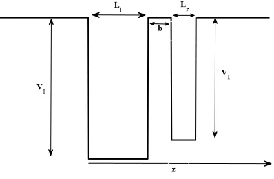
As the PSO algorithm is a random statistical algorithm, the typical con-vergence plots of PSO for nding optimal absorption for 50 iterations is shown in Fig.2. In this figure shows that by using the PSO algorithm after 20 it-eration optical rectification coefficient has a constant value which is equal to 1.30390×10⁵Arb.U nits.
0 5 10 15 20 25 30 35 40 45 50
2 4 6 8 10 12 14x 10
4
Iteration
Cross Section (Arb. Units)
Figure 2: Convergence plot of PSO for nding optimal ERS.
The optimum structure of double quantum wells depicts in Fig.3. includes the wave functions of ASDQWs. Seen that optimum structure is asymmetric and using the numerical solutions.
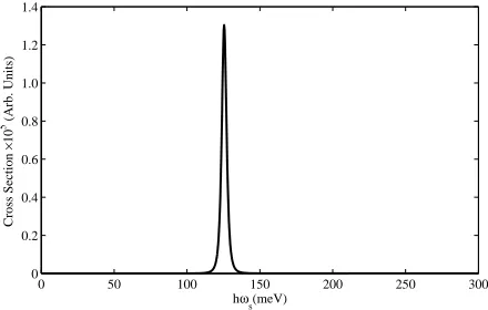
Fig.4 display the ERS as a function of secondary radiation photon energy
ℏωsfor our optimal structure. This indicates that resonant peak at photon energy value of 125.498 (meV) as expected corresponding to the is ℏωs =
E3−E2 and non-resonant peak at photon energy value of 125.473 (meV) as expected corresponding to the is ℏωs=ℏωl+E3−E2. From this figure we see that resonant and non-resonant are overlapping and the magnitude of the non-resonant peak is 1.30390×10⁵Arb.U nits. We should note that the
−1000 −50 0 50 100 150 200 0.05
0.1 0.15 0.2 0.25 0.3 0.35 0.4 0.45
z(A°)
ψ2 ψ3
ψ1
Figure 3: Schematic diagram for an asymmetric double quantum well for optimal parameters with wave function.
0 50 100 150 200 250 300
0 0.2 0.4 0.6 0.8 1.0 1.2 1.4
hω s(meV)
Cross Section
×
10
5 (Arb. Units)
Figure 4: Schematic diagram for an asymmetric double quantum well for optimal parameters with wave function.
4 Conclusion
Acknowledgements
The authors would like to express their special gratitude to the Shiraz Uni-versity of Technology.
References
1. Betancourt-Riera, R., Riera, R. and Rosas, R. Electron Raman scat-tering in asymmetrical multiple quantum wells system with an external
electric field.Physica E: Low-dimensional Systems and Nanostructures,
44 (2012), 1152–1157.
2. Betancourt-Riera, R., Rosas, R., Marn-Enriquez, I., Riera, R. and Marin, J. L.Electron Raman scattering in asymmetrical multiple quantum wells.
Journal of Physics: Condensed Matter, 17 (2005), 4451–4461.
3. Cardona, M.Lattice vibrations in semiconductor superlattices. Superlat-tices and microstructures, 7 (1990), 183–192.
4. Cardona, M. and Guntherodt, G.Light Scattering in Solids V (Topics in
Applied Physics 66), Springer, Heidelberg, 1989.
5. Comas, F., Trallero-Giner, C. and Perez-Alvarez, R.Interband-intraband
electronic Raman scattering in semiconductors. Journal of Physics C:
Solid State Physics, 19 (1986), 6479–6488.
6. Ismailov, T. G. and Mehdiyev, B. H. Electron Raman scattering in a
cylindrical quantum dot in a magnetic field.Physica E: Low-dimensional
Systems and Nanostructures, 31 (2006), 72–77.
7. Kennedy, J. and Eberhart, R. Particle swarm optimization. In Neu-ral Networks, 1995. Proceedings., IEEE International Conference on, 4 (1995), 1942–1948.
8. Khurgin, J. B., Sun, G., Friedman, L. R. and Soref, R. A.Comparative analysis of optically pumped intersubband lasers and intersubband Raman
oscillators.Journal of applied physics, 78 (1995), 7398–7400.
9. Klein, M. Phonons in semiconductor superlattices. IEEE Journal of Quantum Electronics, 22 (1986), 1760-1770.
10. Liu, A. and Ning, C. Z. Terahertz optical gain based on intersubband transitions in optically pumped semiconductor quantum wells: Coherent
11. Riera, R., Comas, F., Trallero Giner, C. and Pavlov, S. T.Electron
Ra-man scattering in semiconductor quantum wells.physica status solidi (b),
148 (1988), 533–542.
12. Sun, G., Khurgin, J. B., Friedman, L. R. and Soref, R. A.Tunable
inter-subband Raman laser in GaAs/AlGaAs multiple quantum wells. JOSA
B, 15 (1998), 648–651.
13. Xie, W. Electron Raman scattering of a two-dimensional pseudodot sys-tem.Physics Letters A, 376 (2012), 1660–1657.
14. Zhao, X. and Liu, C.”One-phonon resonant Raman scattering in
cylin-drical quantum wires.Physica E: Low-dimensional Systems and