https://doi.org/10.5194/ars-15-107-2017
© Author(s) 2017. This work is distributed under the Creative Commons Attribution 3.0 License.
Implementation of envelope detection based Wake-Up Receiver
for IEEE 802.15.4 WPAN from off-the-shelf components
Josua Arndt, Lukas Krystofiak, Vahid Bonehi, Ralf Wunderlich, and Stefan Heinen RWTH Aachen University, Integrated Analog Circuits and RF Systems, 52074 Aachen, Germany
Correspondence to:Josua Arndt ([email protected])
Received: 2 November 2016 – Revised: 1 March 2017 – Accepted: 22 April 2017 – Published: 21 September 2017
Abstract. Power consumption in wireless networks is cru-cial. In most scenarios the transmission time is short com-pared to the idle listening time for data transmission, the most power is consumed by the receiver. In low latency systems there is a need for low power wake-up receivers (WuRx) that reduce the power consumption when the node is idle, but keep it responsive. This work presents a WuRx designed out of commercial components to investigate the needs of a WuRx when it is embedded in a Wireless Personal Area Network (WPAN) system in a real environment setup includ-ing WLAN and LTE communication and considerinclud-ing inter-ferer rejection. The calculation necessary for the attenuation of those interferers is explained in detail. Furthermore, a sys-tem design is presented that fulfills the requirements for this environment and is build from off-the-shelf components.
1 Introduction
Personal Area Networks, as specified by (Gutierrez et al., 2003), applications like lighting control, monitoring temper-ature, moisture etc. or IoT (Internet of Things) devices can demand a fast reaction in lighting systems for example. If the user activates the light it should react in milliseconds as we are used to the lights switching on instantly. For those ap-plications, the receiver must always be active to listen to the channel. In beacon-enabled networks a fast reaction time can be achieved by a big duty-cycle, resulting in a high beacon number to send. The end devices must wake up frequently which results in a high-energy consumption. A WuRx de-signed to support a low data rate modulation can be very simple and consumes less energy than a high data rate mod-ulation like BPSK or O-QPSK.
Conventional receiver architectures are the heterodyne or homodyne (zero-IF) receiver which support complex modu-lation schemes whereby a high spectral efficiency and at last a high data rate can be achieved. Both rely on at least one LO (Local Oscillator) which commonly consists of a LC os-cillator embedded in a power consuming PLL (phase-locked loop) with an operating frequency in the RF range. A regen-erative circuit as alternative receiver concept is tempting be-cause it only oscillates when there is a signal at the input, but the bias current of the of the LC circuit is the main problem in reducing power dissipation. Last there is the direct con-version by an envelope detector, which shows potential for a very low power consumption.
A WuRx using the conventional heterodyne receiver con-cept architecture is presented in (Pletcher et al., 2008), the power consumption splits up as follows: RF Amplification 22, LO 20, Mixer 8 and the ED 1 µW. A LO-less approach using a double-sampling technique to suppress the offset and 1/f noise of the down-converting envelope detector is pre-sented in (Huang et al., 2010). The power consumption can be divided as follows: LNA 27 µW, BB-amplifier 14 µW, ED 5 µW, bias circuit 4 µW, frequency divider and logic 3 µW, external reference clock 1 µW. In (Hambeck et al., 2011) a direct down conversion concept is shown, the power con-sumption on this receiver is as follows: ED 1.25 µW, BB-amplifier 0.4 µW, correlation unit 0.4 µW and the RC low-pass filter 0.2 µW. Comparing the power dissipation of these wake-up receivers shows that a very low power dissipation can be achieved with the direct conversion approach.
based WuRx was also developed to be used as a first proto-type to implement a full functioning IEEE 802.15.4 network. The Development of on SOC with design, implementation, tape-out and design of a measurement PCB, debug and mea-sure the SOC and develop an application PCB takes up to 3 years. Therefore, a WuRx out of commercial components is built on PCB to investigate the needs of a system that in-cludes a WuRx and uses the IEEE 802.15.4 transmitter to generate the wake-up frame. Challenges will be discussed and solutions presented.
As IEEE 802.15.4 transmitter we used the AT86RF233 from (Atmel, 2014) which is a high-performance RF-CMOS 2.4 GHz radio transceiver targeted for IEEE 802.15.4, Zig-Bee, RF4CE, 6LoWPAN, and ISM applications. It has a re-ceiver sensitivity of−101 dBm and a programmable TX out-put power from−17 to 4 dBm.
In Sect. 2 an overview of the requirements will be given and basics of path loss and link margin calculations are pre-sented. In Sect. 3 the system setup, filter design and resulting link budget are presented. In Sect. 4 the measurements of the WuRx are shown and Sect. 5 concludes the paper.
2 Design requirements
As the comparison in (Oetting, 1979) shows, on-off-keying (OOK) is the simplest modulation scheme for digital radio transmission. A tuned RF receiver is one of the simplest architectures (Griggs, 2012). It accepts incoming RF sig-nals which are filtered, amplified and converted from RF to baseband by an envelope detector (ED). This eliminates the need for a power consuming local oscillator (LO) completely, which is usually the most power consuming component in a receiver; as shown in the previews comparison of state-of-the-art WuRx.
However, this means that this receiver can process ampli-tude modulated signals only and the architecture calls for a very high selectivity at RF, which will be explained later in detail. This is a result of the behavior of the ED converting all signals directly to baseband without filtering.
The designated transmit distance of our WPAN net-works with WuRx is between 5 and 30 m indoors. In our scenario, the WuRx works at the same frequency as the main transceiver. To reduce hardware complexity, the main transceiver will be used to generate the OOK signal.
As widely known, a higher carrier frequency enables broader bandwidth and therefore a high data rate as well as reduced diffraction loss, smaller antenna size and overall in-creased level of integration.
However, a higher carrier frequency also increases the path loss and therefore the necessary sensitivity of the receiver. Moreover, additional filtering and amplification at high fre-quencies is more complex and power hungry. The formula
for free space path loss is:
Ls
dB =10 log10 4
π d λ
2
=20 log10 4
πf d c
=20 log10(d)+20 log10(f )−147.55
(1)
with the carrier wavelength λ(m), the carrier frequency
f(Hz), the speed of light c(m s−1) and the link distance
d(m). To calculate the path loss, we consider a direct line of sight and no walls and floors, which is equal to a large room. As shown by (Heereman et al., 2011) the path loss ex-ponent then is smaller than 2, so for simplicity we can use the simple free space path loss equation formula.
Hence with a carrier frequency of 2.48 GHz and a link dis-tance of 10 m the path loss would be 70 dB, at 30 m roughly 80 dB. A better insight of indoor wireless coverage can be found in (Plets et al., 2013). For WLAN at 2.467 GHz and a distance of 1 m the result isLs= −40 dB which is an atten-uation of 40 dB.
Inserting the system specific transmit powerPTX[dB] and the ED sensitivitySED[dB] we can calculate the resulting link margin LM[dB]. This can be interpreted as the addi-tional gain necessary to be able to detect a signal at the in-serted frequency and distance.
LM
dB =PTX−SED
−20 log10(d)−20 log10(f )+147.55
(2)
Setting the link margin to zero and solving the equation for
dgives the distance at which the signal can be detected, or at which an interferer can no longer disturb.
d=10(PTX−SED−20 log10(f )+147.55)/20 (3)
Also, considering the overall gainG[dB] and interferer at-tenuationAI[dB] of the system and solving the equation for
AI[dB] we can calculate the necessary attenuation for an in-terferer in a dedicated distance.
AI
dB =PTX−SED+G
−20 log10(d)−20 log10(f )+147.55
(4)
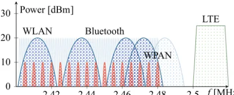
Figure 1 shows the ISM and LTE Band allocation for WLAN, Bluetooth, WPAN and LTE Band 7. As shown the ISM Band is used by a lot of participants in different chan-nels. Bluetooth uses 1 MHz channels and frequency hopping so collision with a Bluetooth device should not occur too often and only for short times. WLAN uses 20 or 40 MHz channels, e.g. when a video is streamed the channel is used continuously, this interferer has to be suppressed as much as possible. LTE Band 7 is used for mobile communication. It also uses a high bandwidth and a higher transmit power.
2.42 2.44 2.46 2.48 2.5 0
10 20 30
WLAN
LTE
WPAN Bluetooth
f[MHz] Power [dBm]
Figure 1.ISM and LTE band 7 allocation.
− 10 − 5 0 5 10 ·106 0
10 20
30 Power [dB]
2.46 2.48 2.5 2.52 ·109 WLAN
LTE
WPAN f
Figure 2.Down conversion of RF signals to baseband by envelop detection with WLAN and LTE communication as interference.
Figure 2 illustrates the down-conversion of the RF band to baseband by an ED containing the wake-up signal on WPAN channel 26 and the two closest interferers, WLAN channel 13 and LTE band 7. As shown in the illustration the interfer-ers potentially have a higher transmit power than our WPAN node, which is specified for the AT68RF233 as 4 dBm with-out losses due to the balloon, the antenna or mismatch.
As defined in (IEEE 802.11b, 2000), the maximum trans-mit power of WLAN is 20 dBm and LTE band 7 user equip-ment and base stations are limited to 24 dBm as defined in (ETSI TS 136 101, 2014) and (ETSI TS 136 104, 2010). All-ready mentioned earlier a narrowband filter in the RF band is necessary to suppress interferers and converts down only the band of interest to be able to detect the signal with the ED. Calculating the attenuation needed to suppress WLAN with a transmit power of 20 dBm at a distance of 1 m for a system using an ED with a sensitivity of−30 dBm results in approx-imately 10 dB and for LTE with 24 dBm transmit power in 13.7 dB, according to Eq. (4).
3 System design 3.1 System setup
For this work the absolute power consumption of the system is not important since it cannot compete with integrated so-lutions anyway. The emphasis is on the knowledge gained on how parts influence each other, System feasibility and usabil-ity in a real world application.
Figure 3.WuRx system concept with overlapping filters to gain an extremely narrowband filtering.
All parts had to be chosen to allow for manual soldering for fast adaption of changes and debugging.
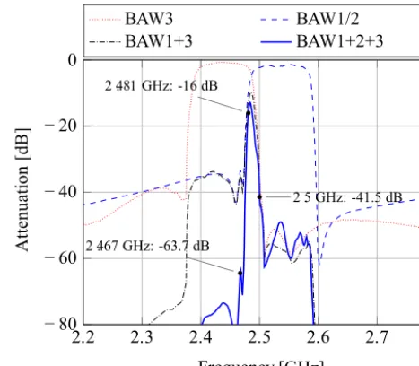
Figure 3 shows the different stages of the WuRx. To achieve a good interferer suppression, we designed the WuRx using multiple bulk acoustic wave (BAW) filters with differ-ent pass characteristics, which will be explained later.
The WuRx sensitivity suffers heavily from the additional attenuation of the bandpass filter configuration. Increased gain is the only way to increase the sensitivity, but amplifica-tion comes with the cost of power consumpamplifica-tion in general.
The LNA SKY67159-396LF from Skyworks has promis-ing features but was not commercially available at the time. Skyworks provided some samples, we decided to not rely on this LNA only and used another amplifier for the 2 and 3 stage. The SKY67159-396LF is a broadband amplifier, that works from 200 MHz to 3800 MHz, has a gain of 17 dB and a very low noise figure of approximately 1 dB.
HMC414, PA1 and PA2, manufactured by Hittite Mi-crowave Products (HMC) designed for frequencies between 2.2 and 2.8 GHz has a gain of up to 20 dB, a noise figure of 6.5 dB and enable-times in the nanosecond time scale.
Additionally, the output current can be set by dedicated pins and can be reduced as much as possible without influ-encing the sensitivity.
Table 1.Data sheet specifications at 25◦C, 3.3 V, 2.481 GHz.
Current Gain
mA dB
LNA 45.5 17.2
Power Amplifier1+2 494∗ 34 Envelope Detector 0.55 –
Comparator 0.275 –
Total 540.3 51.2
∗Absolute power consumption is not focus of this work.
The last active component of the front-end is a comparator which serves as 1-bit ADC. The requirements are very low since the wake-up signal is in baseband at this stage and has a fairly low data rate of 1 kHz. It should have a pin to latch the output.
The used comparator is a MAX9141 produced by Maxim Integrated. It is a low power, high speed device and exceeds the needed requirements. The data sheet states a propagation delay of 140 ns, a latch delay of 16 ns for setup and hold time and a latch propagation delay of 60 ns.
It features an internal hysteresis of about 1.5 mV; this en-sures clean switching even with slow moving input signals generated by the ED. The threshold at which the compara-tor switches from 0.3 to 3 V is adjustable. Its value depends on the dc offset of the ED, the received signal strength od the wake-up signal, the gain of the WuRx and the received signal strength of the interferer.
An extraction of some interesting characteristics of the parts used are listed in Table 1, taken from the data sheets.
3.2 Narrowband filter
As mentioned earlier the interferers potentially have a higher power than the wanted signal which leads to the necessity of strong suppression. To achieve the necessary interferer rejection, a combination of multiple BAW filters are used, which have an overlapping frequency range in the designated area. For a cheap WuRx BAW filter will not be feasible, so in the concept of the integrated version the interferer rejec-tion should be addressed by selective amplificarejec-tion and low power filter concepts.
More information about BAW filters can be found in (Ma-hon and Aigner, 2007). We choose two BAW filters from Triquint, BAW 885033 (fc=2.442 MHz, BAW3) and BAW 885009 (fc=2.535 MHz, BAW1/2). The BAW 885033 has a bandwidth of 79 MHz and for the desired frequency of 2.481 GHz it has an insertion loss of 1.7 to 2.2 dB as shown in Fig. 4. It creates the upper cut-off-frequency for interferers, especially LTE in Germany, starting at 2.5 GHz. According to the data sheet the attenuation at 2.5 GHz is around 40 dB at 25◦C. The BAW 885009 filter used as BAW1/2 shown in Fig. 4 forms the lower cut-off frequency and has a bandwidth
2.2 2.3 2.4 2.5 2.6 2.7 2.8 0
− 20
− 40
− 60
− 80
2 .481 GHz: -16 dB
2 .467 GHz: -63.7 dB
2 .5 GHz: -41.5 dB
Frequency [GHz]
A
tt
en
ua
ti
on
[d
B
]
BAW3 BAW1/2
BAW1+3 BAW1+2+3
Figure 4.SimulatedS21-parameter of the BAW filters and their combinations.
of 70 MHz. The desired frequency lies at the lower edge of this filter and is attenuated by about 9.5 dB. Undesired fre-quencies that go up to 2.473 GHz will be attenuated by at least 33 dB. Unfortunately there were noS-parameter files provided for the BAW 885033 so theS-parameters of a BAW filter from the same manufacturer, that comes very close to the used one are shown in Fig. 4 for simulation and visual-ization.
Combining the two filters (BAW1+3) results in the char-acteristic as shown in Fi. 4. Calculated values result in an attenuation of 12.6 dB for 2.481 GHz, of 34.8 dB for 2.467 GHz and of 39.1 dB for 2.5 GHz. With a gain of 51.5 dB this would result in approx. 11 m distance needed to the next WLAN router and 17 m to the next LTE device. This is not sufficient for our scenario, as coexistence with at least WLAN should be possible.
Subsequently, an additional filter, BAW2, with a centre frequency at 2.535 GHz was used.
The plots for BAW3, BAW1/2 and BAW1+3 are made using unmatched components to get a general overview of the behavior. In a last step, a matching network was designed to increase performance for the frequency used.
WLAN 0.4 m LTE 8.3 m WPAN 15.8 m
Figure 5.Min. interferer and max. transmitter distance.
to 63.7 dB at 2.467 GHz and at 2.5 GHz by around 1.5 to 41.5 dB, as marked in Fig. 4. Consequently, the distance to WLAN reduces to 0.7 m and for LTE to 14.8 m. Adding more attenuation for LTE would have added too much attenuation to the desired signal. With the choosen 3 filter configuration the system will still be error prone for LTE, but sufficiently robust against WLAN.
3.3 Link margin
In Fig. 5 the minimal distances for WLAN, LTE and the max-imum distance for the transmitter and the WuRX are shown. Calculating the link margin has been done repeatedly throughout the work to evaluate the results of this approach. The final performance presented here is achieved with simu-lated data of the architecture and components described be-fore. With a sensitivity of −25 dBm of the ED, a gain of about 35.2 dB of the amplifier and filter stage, we get a sensi-tivity of−60.2 dBm at 2.481 GHz. With an assumed radiated output power of 4 dBm the equation for path loss gives an ideal maximum link distance of around 15.6 m.
This will be reduced by the small output swing of the ED and noise at the input of the ED, which effect the configura-tion of the threshold voltage of the comparator. Considering the output offset of the ED a reasonable start value for the threshold of the comparator is 280 mV at the output of the ED. The minimum distance is also limited by the ED with an upper limit of 12 dBm, that can be detected. This leads to a minimum distance of around 0.2 m.
The input compression of the amplifiers is not be reached at this point with these components. With the maximum radi-ation power of 20 dBm and an attenuradi-ation of 12.5 dB WLAN signals will not disturb at a distance of around 0.4 m.
Depending on the distance of the base station the radiation power for mobile phones can reach up to 24 dBm as specified in the 3G standard, to which LTE belongs (3.9G). The uplink frequencies for LTE vary from 2.5 GHz up to 2.57 GHz in Germany. With a total gain of 10 dB for LTE frequencies, these signals overshadow the desired signal significantly at the same distance to the receiver.
A minimum distance of 8.3 m to the LTE transmitter is necessary prevent corruption of the wake-up sequence. To coexist closer to LTE, we can adjust the threshold of the
com-Table 2.Measured electric specifications, 3.3 V
Current Gain @ 2.481 GHz
mA dB
BAW 1+2+3 – – 16
LNA 45.5 13.35
Power Amplifier 1 71.91,2 12.82 Power Amplifier 2 731,2 12.21
Envelope Detector 0.55 –
Comparator 0.165 –
Total 191 22.38
1Absolute power consumption is not focus of this work. 2With optimized output current configuration.
2.2 2.3 2.4 2.5 2.6 2.7 2.8
35
25
15
5 − 5
− 15
− 25
− 35
− 45
2.481 GHz: 25.95 dB
2.467 GHz: -19.05 dB
2.5 GHz: 3 dB
Frequency [GHz]
G
ai
n
[d
B
]
Figure 6.Measured gain of the complete WuRx
parator, which results in a reduced maximum distance of the wake-up receiver to the transmitter.
4 Implementation and measurements
To debug the WuRx every stage was soldered and measured successively. As expected, the comparison of simulated and the measured values differ and each stage had to be matched with regard to the measured values again. Some selected measurements are listed in Table 2.
All stages showed lower performance than listed in the data sheet, which is caused by the FR4 substrate of the PCB. The data sheets and application notes are based on Roger substrate and the data sheet values also take board loss deem-bedding into account. Our measurements include all losses only deembedding the cable losses by calibration.
Figure 7.Wake-up receiver PCB.
the maximal gain could not be used. Thus, the gain of the HMC414 is not as high as expected.
The Application note from the (Hittite Microwave Corpo-ration, 2004) addressing this problem helped to solve this is-sue but was found while debugging. The solutions and im-provements shown there could not be implemented on the board to gain the best performance.
Figure 6 shows a measurement of the whole circuit from the SMA connector to the output of the last amplifier. The in-crease of 3 dB from single component to whole system mea-surement can be explained by better matching of the stages to each other than to the measurement equipment.
Considering optimum matching and operating power am-plifiers the general functionality of the circuit was tested. For the baseband output voltage of the ED we get a value of about 275 mV with no incoming RF signal. With regard to the in-put hysteresis and offset of the comparator the voltage is ad-justed to make sure it switches only if a signal is present. This threshold is found to be at 284 mV. With a signal generator directly connected to the board, the sensitivity at 2.481 GHz is−20.0 dBm. With a gain of 26 dB this results in an ideal range of about 3 m with an output power of 4 dBm of the transmitter. For 2.467 GHz we have an attenuation of 19 dB and for 2.5 GHz a gain of 3 dB.
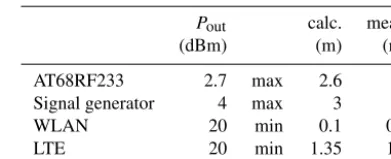
Table 3 shows the calculated distance using the mea-sured gain and sensitivity values and the meamea-sured distance achieved with a signal generator and a transmitter board with an AT86RF233. Interferer rejection was tested by applying the signal from the generator to an antenna.
5 Conclusions
In this work, we showed the implementation of a wake-up re-ceiver with commercial components to investigate the needs of such a system. It uses discrete off-the-shelf components and was built on a FR4 PCB to have the possibility to mea-sure and analyze the state of the signal after every step. It
Table 3.Calculated and measured range and interferer rejection.
Pout calc. meas.
(dBm) (m) (m)
AT68RF233 2.7 max 2.6 2
Signal generator 4 max 3 3
WLAN 20 min 0.1 0.3
LTE 20 min 1.35 1.6
will be mounted on a board with a RF transceiver and a mi-crocontroller.
Due to the lack of selectivity of the components used in the circuit, high-Q bandpass filtering had to be implemented to make sure that the receiver works reliably in the 2.4 GHz band. These three successive BAW filters were used to form a narrow bandpass filter and reject even strong out-of-band interferers. The increased losses had to be compensated with additional gain stages. We designed the circuit with a sensi-tivity of−60 dBm, while still being able to detect a signal in close approximation to interferers sources.
Due to mismatch and oscillation problems, measurements showed a reduced sensitivity of only−47 dBm. However, the attenuation of out-of-band interferers stayed in the same re-lation to the gain for the desired signal.
This work shows an implementation of an envelope-detection-based WuRx with off-the-shelf components which fulfills the requirements of a real-world application. The fur-ther development will be the implementation of a network with this WuRx and investigate how the AT86RF233 can be used to generate the wake-up signal, to investigate the system network setup. The goal of this work was to get better insight in the overall system and the obstacles, gained knowledge by the development is included to the integrated designs.
Data availability. The gain simulation and measurement results are available at Zenodo (Arndt, 2017).
Competing interests. The authors declare that they have no conflict of interest.
Acknowledgements. The authors acknowledge the support of the German Federal Ministry of Education and Research (BMBF) through the “TreuFunk” project (FKZ: 16KIS0234).
Edited by: J. Anders
References
Arndt, J.: Implementation of envelope detection based Wake-Up Receiver for IEEE 802.15.4 WPAN from off-the-shelf compo-nents,https://doi.org/10.5281/zenodo.582796, 2017.
Atmel: AT86RF233 Low Power, 2.4 GHz Transceiver for ZigBee, RF4CE, IEEE 802.15.4, 6LoWPAN, and ISM Applica-tions, http://ww1.microchip.com/downloads/en/DeviceDoc/ Atmel-8351-MCU_Wireless-AT86RF233_Datasheet.pdf, 2014. ETSI TS 136 101, T. S.: ETSI TS 136 101 V12.5.0 (2014-11), LTE;Evolved Universal Terrestrial Radio Access (E-UTRA); User Equipment (UE) radio transmission and reception (3GPP TS 36.101 version 12.5.0 Release 12), 2014.
ETSI TS 136 104, T. S.: ETSI TS 136 104 V9.4.0 (2010-07), LTE; Evolved Universal Terrestrial Radio Access (E-UTRA); Base Station (BS) radio transmission and reception (3GPP TS 36.104 version 9.4.0 Release 9), 2010.
Griggs, J. D.: Ultra-Low Power Wake up Receiver for Medical Im-plant Communications Service Transceiver, Ph.D. thesis, North Carolina A&T State University, 2012.
Gutierrez, J. A., Callaway, E. H., and Barrett, R.: IEEE 802.15.4 Low-Rate Wireless Personal Area Networks: Enabling Wireless Sensor Networks, IEEE Standards Office, New York, NY, USA, 2003.
Hambeck, C., Mahlknecht, S., and Herndl, T.: A 2.4 µW Wake-up Receiver for wireless sensor nodes with
−71 dBm sensitivity, in: 2011 IEEE International Sym-posium of Circuits and Systems (ISCAS), 534–537, https://doi.org/10.1109/ISCAS.2011.5937620, 2011.
Heereman, F., Joseph, W., Tanghe, E., Plets, D., and Martens, L.: Prediction of range, power consumption and throughput for IEEE 802.11n in large conference rooms, in: Proceedings of the 5th European Conference on Antennas and Propagation (EUCAP), 692–696, 2011.
Hittite Microwave Corporation, A. D.: Designing w/The HMC414MS8G PA Utilizing a Low Cost Laminated Printed Circuit Board, 2004.
Huang, X., Rampu, S., Wang, X., Dolmans, G., and de Groot, H.: A 2.4 GHz/915 MHz 51 µW wake-up receiver with off-set and noise suppression, in: 2010 IEEE International Solid-State Circuits Conference – (ISSCC), 222–223, https://doi.org/10.1109/ISSCC.2010.5433958, 2010.
IEEE 802.11b: IEEE Standard for Information Technology – Telecommunications and information exchange between sys-tems – Local and Metropolitan networks – Specific requirements – Part 11: Wireless LAN Medium Access Control (MAC) and Physical Layer (PHY) specifications: Higher Speed Physical Layer (PHY) Extension in the 2.4 GHz band, IEEE Std 802.11b-1999, 1–96, https://doi.org/10.1109/IEEESTD.2000.90914, 2000.
Mahon, S. and Aigner, R.: Bulk Acoustic Wave Devices – Why, How, and Where They are Going, in: CS MANTECH Confer-ence, 2007.
Oetting, J.: A Comparison of Modulation Techniques for Digital Radio, IEEE T. Commun., 27, 1752–1762, https://doi.org/10.1109/TCOM.1979.1094370, 1979.
Pletcher, N. M., Gambini, S., and Rabaey, J. M.: A 2 GHz 52 µW Wake-Up Receiver with −72 dBm Sensitivity Using Uncertain-IF Architecture, in: 2008 IEEE International Solid-State Circuits Conference – Digest of Technical Papers, 524– 633, https://doi.org/10.1109/ISSCC.2008.4523288, 2008. Plets, D., Joseph, W., Vanhecke, K., Tanghe, E., and Martens,