https://doi.org/10.5194/ars-17-239-2019
© Author(s) 2019. This work is distributed under the Creative Commons Attribution 4.0 License.
Realization and opto-electronic Characterization of linear Self-Reset
Pixel Cells for a high dynamic CMOS Image Sensor
Stefan Hirsch, Markus Strobel, Wolfram Klingler, Jan Dirk Schulze Spüntrup, Zili Yu, and Joachim N. Burghartz Institut für Mikroelektronik Stuttgart (IMS CHIPS), Allmandring 30a, 70569 Stuttgart, Germany
Correspondence:Stefan Hirsch ([email protected])
Received: 14 February 2019 – Revised: 16 July 2019 – Accepted: 6 September 2019 – Published: 20 September 2019
Abstract. Conventional CMOS image sensors with a lin-ear transfer characteristic only have a limited dynamic range (DR) of about 60–70 dB. To extend the dynamic range con-siderably, the already successfully demonstrated concept of a linear self-reset pixel was employed in this work. With the self-reset concept the limit of the maximum analyzable photo generated charge (Qmax) during the exposure time is extended to a multiple of the saturation charge of the photo diode (Qsat) by asynchronous self-resets of the photo diode. Additionally, the remaining charge at the end of the expo-sure time is evaluated to increase the resolution of the opto-electronic conversion. Thus we achieved pixels with a DR of more than 120 dB combined with an improved low light sensitivity using a pinned photodiode.
This paper focuses on two topics: One is the realiza-tion and opto-electronic characterizarealiza-tion of further self-reset pixel cells for an experimental optimization of the function-ality with respect to linearity and high signal-to-noise ratio. The second one is the assembly and digital readout of a clus-ter structure composed of 16×16 pixel matrix on a CMOS test chip. One constraint for later usage of the pixel cells in a high resolution (>VGA) image sensor is the required layout area of the individual circuit blocks. For the cluster structure a size of 20×20 µm2 for the analog part of the pixel containing the photo diode and the other analog circuit blocks, the comparator and the signal shaping, was desired. The circuit design and layout work included several vari-ants of the pinned photo diode with floating diffusion (FD) readout node, which is also used for analog voltage storage, and different control transistors. Further for the comparator a telescopic differential amplifier with high gain was imple-mented as well as peripheral 10 bit counter/shift register as static and dynamic versions. Test chips have been fabricated
in an advanced 0.18 µm CMOS technology for optical sen-sors with low leakage currents.
The sensor chips have been evaluated with a specifically developed test setup which gives the flexibility to arbitrar-ily generate the digital and analog control signals in terms of timing and voltage levels. Based on this, the number of asyn-chronous self-resets could be read out from the counters of the pixel cells as coarse values. The remaining charge at the end of the integration time was digitized using a ramp ana-log to digital conversion and could be read out as fine values. An opto-electronic characterization with adjustable illumina-tion from 0 lx to 13 klx was done to measure and analyze the opto-electronic conversion function (OECF) and the noise of six different self-reset pixel cells having the high-gain differ-ential amplifier as comparator. Finally the coarse values of two implemented 16×16 pixel clusters could be read out as a mini camera using a lens for optical image formation.
1 Introduction
Applications in the fields of e.g. industrial image processing, image based robotic control systems and autonomous driv-ing require high dynamic range image sensors. This high dy-namic range is needed for robust image capturing and subse-quent image processing. A further requirement from measur-ing point of view is that the image sensor does not only have a linear high dynamic range but also a high signal-to-noise ratio.
240 S. Hirsch et al.: Linear Self-Reset Pixel Cells for a high dynamic CMOS Image Sensor
and low illumination respectively, like multiple-captures of images or dual-/multi-sampling (Kim et al., 2008). Other ap-proaches use lateral-overflow gate for the photodiode sense node (Decker et al., 1998) or lateral-overflow capacitor (Sug-awa et al., 2005) for dual conversion gain readout. All these techniques enhance the DR to about 100 dB while having a reasonable drop of the signal-to-noise ratio (SNR) at the tran-sition between high and low illumination. Logarithmic high dynamic range CMOS (HDRC) imagers exhibit up to 170 dB DR (Höfflinger, 2007; Burghartz et al., 2006) having a bal-anced but lower peak SNR over illumination. A considerably extended DR with linear response is achieved with light-to-frequency conversion (Yang, 1994) and self-reset pixels (Hirsch et al., 2017; Leñero-Bardallo et al., 2017; Peizerat and Arques, 2007; Kavusi et al., 2006; Wang et al., 2006). A DR of nearly 140 dB has been reported for a particular archi-tecture of a self-reset pixel (Kavusi et al., 2006).
Our implementation of the self-reset pixel employing a pinned photodiode will be described in Sect. 2 where the maximum analyzable photo generated charge (Qmax) during the exposure time is extended to a multiple of the saturation charge of the photo diode (Qsat) by asynchronous self-resets of the photo diode. This gives rise to a potentially higher peak SNR at high illumination levels compared to conventional CMOS imagers with 3T or 4T pixel architecture having an equal full well capacity (Qsat). To increase the resolution, the remaining charge of the photo diode at the end of the ex-posure time is analyzed for improved low light sensitivity. We were able to achieve a DR of more than 120 dB using a pinned photodiode with low dark current and floating diffu-sion charge storage node.
The test chip which was designed and realized is explained in Sect. 3. Section 4 presents the measurement setup and the measurement results of the different single pixel cell vari-ants and their opto-electronic characterization. In Sect. 5 the structure of the pixel cluster and its measurement results are shown.
2 Self-reset pixel 2.1 Pixel cell
Each self-reset pixel has an analog and a digital part and for all pixels one global control exists on-chip or off-chip (see Fig. 1). The analog part of the pixel cell is composed of a pinned photo diode, transfer and reset transistors, a floating diffusion (FD) node used as hold element, a comparator with high gain and a delay element with feedback path to reset the floating diffusion node. The advantages of the pinned photo diode are low leakage currents caused by a special pinned layer and an electronic shutter with a transfer gate to the floating diffusion node FD. For evaluation purposes the delay time within the feedback path is variable and can be adjusted from outside the chip by a bias voltage. The two stage
com-parator is quite important for the function of the pixel cell. It has an open loop gain of about 80 dB, is built up of 11 tran-sistors and the input range is adapted to the voltage levels of the floating diffusion node. Its first stage is a telescopic transconductance amplifier. A tradeoff between the needed complexity and the available area for the layout had to be found. The comparator has a current consumption of about 300 nA. The layout of the analog part of the pixel cell needs an area of 20×20 µm2.
The digital part consists of several logic gates and a 10 bit counter which is designed as a linear feedback shift register with ten serially connected D-type flip-flops. The outputs of the seventh and tenth flip-flop are connected to a XNOR gate. In the counting mode the output of the XNOR gate is fed to the input of the first flip-flop whereas in the readout mode the input signal ser_in is connected to the input of the first flip-flop. This is needed to connect the counters of all the pixels of a pixel cluster (see Sect. 5) in series to do the readout of the data and to reset all the counters to zero or to preload to a specific value. The 10 bit counter value is shifted out serially on the signal ser_out. Due to the design of the counter as a linear feedback shift register the data needs to be decoded after readout.
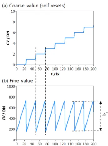
2.2 Conversion concept using the self-reset pixel The self-reset pixel with the analog and digital part was ex-plained in the previous section. For image capturing it oper-ates in four phases as depicted in Fig. 2. After an initial re-set to SVDD the floating diffusion (FD) charge storing node is discharged during the first phase due to the photo current generated by the light exposed photodiode while the transfer gate is switched on. If the node reaches the reference voltage
Vcompit will be reset to SVDD and the value of the counter in the digital part of this pixel is increased by one. This will continue until the end of the integration time of 10 ms. Thus after the end of phase 1 the value of the counter which con-tains the number of self-resets represents a coarse value of the measured light intensity. In phase 2 this counter value is read out and simultaneously the counter is reset to 0. At the end of phase 1 a residue charge remains on the floating diffu-sion node in the pixel, represented by the voltageVFDon this node. This voltage is converted as a fine value of the pixel in phase 3 using a ramp analog to digital conversion. In phase 4 this fine value is read out from the counter and the counter is reset again. The combination of the 10 bit coarse and 10 bit fine values results in a linear 20 bit value.
Figure 1.Schematics of the analog and digital parts of one pixel cell and a global control for all pixel cells.
Figure 2.Working principle of the self-reset pixel.
3 Realized CMOS test chip
The test chip in Fig. 4 was fabricated in an advanced 0.18 µm CMOS technology for optical sensors with low leakage cur-rents. The supply voltage of the analog parts is 3.3 V, the dig-ital parts work with 1.8 V. The following elements have been integrated on the chip: 23 variants of single pixel cells (i), two different 16×16 pixel clusters (ii) and one digital to analog converter (iii). The clusters are described more in detail in Sect. 5. The 23 variants of single pixel cells are composed of different types of photo diodes (differences in layout), tran-sistors (different threshold voltages), comparators (different topology), delay elements and counters/shift registers (static, dynamic, quasi static, static with latch). The reason of the
different pixel variants will be addressed in more detail in the next paragraph. In the final implementation the digital to analog converter shall create the variable reference volt-age (constant in phase 1, linear ramp in phase 3) at the node v_comp which is connected to the inverting input of the com-parator in the self-reset pixels and used in the phases 1 and 3. To be more flexible during evaluation of the pixel cells in this test chip the reference voltage v_comp is not generated with the on chip DAC but by means of an external arbitrary waveform generator.
242 S. Hirsch et al.: Linear Self-Reset Pixel Cells for a high dynamic CMOS Image Sensor
Figure 3. (a)Coarse and(b)fine value as a function of illumination.
Figure 4.Realized CMOS test chip:(a)photograph of the packaged chip,(b)screenshot of the layout.
lists the pixel differences of the photodiode related transistors pixTG and sRST, the floating diffusion (FD) capacitance, the photodiode (PD) area and fill factor (in respect to the analog area of 20×20 µm2). Regular (RVT) or low (LVT) threshold voltage of transistor sRST (during phase 1) and pixTG (at the end of phase 1) give rise to a voltage shift on FD node through channel charge injection and clock feedthrough of the switched transistor gate in relation to the capacitance of the FD node (Razavi, 2001). Since the FD node voltage de-termines the transition point in time of the comparator output this is a sensitive implementation criterion. Also the leakage currents of the FD node itself, the connected transistors and the photodiode have impact on the FD node voltage during the phases 1–3 and hence on functional and optical perfor-mance. Other differences between the pixels concern the de-lay element and the de-layout pattern of analog pixel circuits.
Table 1.Realized self-reset pixel variants with high gain compara-tor using different photodiode related transiscompara-tor types (RVT regular, LVT low threshold voltage) and design parameters of floating dif-fusion (FD) and photodiode (PD).
Pixel pixTG sRST FD PD PD
Variant Threshold Threshold Capacitance Area Fill Factor
Voltage Voltage (fF) (µm2) (%)
18 LVT LVT 3.7 52.5 13.1
19 RVT LVT 3.7 52.5 13.1
20 RVT LVT 3.8 54.5 13.6
21 RVT RVT 3.8 54.5 13.6
22 RVT RVT 3.7 52.5 13.1
23 RVT RVT 3.7 52.5 13.1
4 Measurement 4.1 Measurement setup
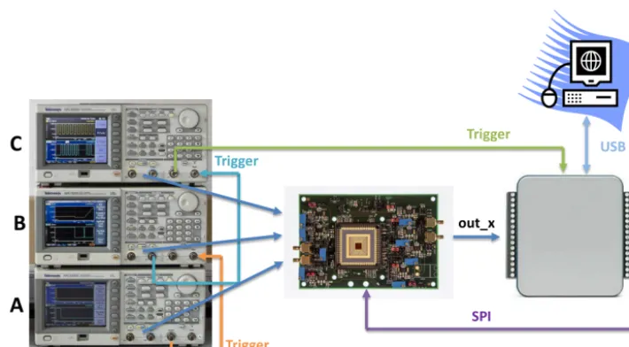
Figure 5 shows the principle of the measurement setup which was developed for the evaluation of the pixel cells variants shown in Fig. 4 part i. The time critical “analog” pixel sig-nals pixRST, pixTG, pixFB and also the signal v_comp (in-cluding the analog ramp for phase 3) are externally driven by three programmable (arbitrary) waveform generators. Ba-sically the pixel signals pixTG/RST/FB are digital signals with a high and low level only, but for the evaluation of the pixel cells the timing, the voltage levels and the rise and fall times are also important. Using the waveform generators here gives the required flexibility. The digital coarse and fine val-ues need to be transferred during the phases 2 and 4 from the counter/shift register in the pixel cells to the PC for a com-puter based analysis of the data. This transfer is done with a mixed signal I/O (input/output) measurement box connected via USB interface with the PC. Especially the readout in phase 2 has to be done quite fast in less than 0.1 ms to avoid too much loss of charge from the floating diffusion node due to parasitic leakage current during this readout time. The variable illumination of the pixel cells is done by a controlled light source with intensity between 1 lx and 13 klx including 0 lx (light source off). The test chip was bonded into an 84 pin ceramic package and inserted in an evaluation board. On this board several voltages to be applied to the chip can be generated by voltage regulators or by digital to analog con-verters. Furthermore the chip signals can be easily accessed for measurement and stimulation. The voltage swing1VFD of the node FD was set to 425 mV in phase 1 and the ramp of the signalVcompin phase 3 had a swing of 1.7 V.
4.2 Opto-electronic characterization
Figure 5.Measurement setup.
coarse values (number of self-resets during phase 1) and 16 fine values (representing the remaining voltage of the node FD at the end of phase 1) is available. For the analysis of the data the average (or median) of the 16 coarse and 16 fine values is calculated. The standard deviation of the 16 fine val-ues determines the temporal noise figure at each illumination level (note: exclusion of outliers at transitions between two adjacent coarse values and median filtering has to be applied to calculated noise curves).
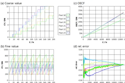
Figure 6a shows the measured (median) coarse values and Fig. 6b the fine values for low illuminations 0–200 lx of the total range 0–13 klx. Compared to Fig. 3 the principle be-havior is as expected but with differences in CV-slopes, FV-offsets and1FV-amplitudes for the six pixel variants which are due to different pixel design parameters shown in Table 1.
1FV-amplitudes are determined for each pixel individually (see Fig. 6b in comparison to Fig. 3) and are given in Ta-ble 2 together with the temporal dark noise SD0, noise SD1 at 100 lx, responsivity R and extracted sensitivityS. Addi-tionally the input offset voltage of the comparators, which is expected within the range of±100 mV, has impact on the CV-slopes and FV-offsets and will give rise to fixed-pattern noise (correctable static pixel-to-pixel variations) in an image sensor.
Combining the measured coarse and fine values for each il-lumination of the total range 0–13 klx results in a linear opto-electronic conversion function (OECF), given in Eq. (1):
OECF(E)=CV(E)·1FV+FV(E), (1)
where CV(E)means the number of coarse values at the illu-minationE, FV(E)is the number of fine values at the illu-minationEand1FV is the amplitude of the saw tooth like curve of the fine value as introduced in Fig. 3.
Figure 6c shows the calculated OECF using Eq. (1) for each pixel variant with fine-tuned amplitude1FV from
Ta-ble 2 over the measured illumination range 0–13 klx. Fine tuning of 1FV was done such, that the calculated OECF curve is continuous at transition points at illuminations where CV has a positive step (by 1) while FV has a negative step (by−1FV) as one can recognize in Fig. 6a and b.
The deviation from linearity of the OECF can be calcu-lated as given in Eq. (2):
rel Error(E)=OECF(E)−RSL(E)
RSL(E) , (2)
where RSL(E)is the reference straight line connecting the start and ending point of the OECF at minimum and maxi-mum illumination. With Eq. (2) Fig. 6d shows the rel. error with a deviation from linearity less than±5 % for all pixel variants over the measured illumination range 0–13 klx.
244 S. Hirsch et al.: Linear Self-Reset Pixel Cells for a high dynamic CMOS Image Sensor
Figure 6.Measured Coarse(a)and Fine Values(b)for 0–200 lx and the calculated OECF(c)with deviation from linearity(d)over the whole illumination range for the six different pixel cell variants 18–23.
Table 2.Measurement results of the opto-electronic characterization for the pixel variants with high gain comparator. Pixel variant 19 (bold font) is the favorite for being integrated in future work.
Pixel Amplitude Dark noise Noise Responsivity Sensitivity Dynamic range Variant 1FV SD0 @ 0 lx SD1 @ 100 lx R S=SD0/R DR
(DN) (DN) (DN) (DN per lx) (lx) (dB)
18 480 0.91 3.3 20.40 0.045 109
19 385 0.27 11.7 24.00 0.011 121
20 415 0.54 6.8 21.90 0.024 115
21 360 0.85 6.7 23.00 0.037 111
22 600 0.65 9.3 24.55 0.026 114
23 330 0.63 24.3 22.85 0.028 113
18 comes from a reduced 1FV value for that pixel due to non-linear distortion which can be seen in the green curve in Fig. 6b for FV>700. Most probably the input stage of the differential comparator is beyond the limit of its linear input voltage range.
The measurement results of major characteristic values for the pixel variants are summarized in Table 2. The pixel vari-ant 19 is the favorite for being integrated in future work. It has a very good sensitivity of 11 mlx @ SNR=1 (Signal-to-Noise Ratio) and tint=10 ms (integration time in phase 1) and a dynamic range of more than 121 dB (note: dynamic range was limited by the maximum possible illumination provided by the measurement setup).
5 Pixel cluster
Figure 7.Layout of the pixel cluster showing details of the pixel cell and the peripheral counter/shift register.
the first counter (SerIn1) to 0 during the readout all counters will be reset to 0 at the end of the readout phase. The one-to-one connection between the analog and digital parts of the pixel cells and the daisy chain connection of the counters is done in that way that the pixels of the cluster are read out line by line from bottom to top and within each line pixel by pixel from left to right. The size of the complete cluster is 960×960 µm2. The second cluster on the chip differs from the first one in such a way that it has an additional buffer be-tween the analog and the digital part to drive the long inter-connect line and to decouple the analog and the digital part to avoid potential crosstalk issues between long interconnecting lines of adjacent pixels. But the measurements have shown no crosstalk issues for both cases.
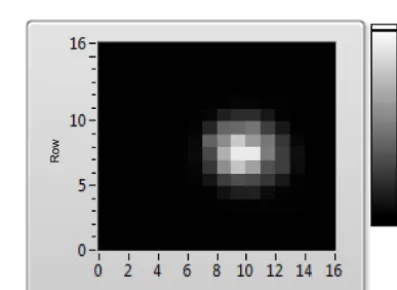
An optical lens with a focal length of 12.5 mm was mounted on top of one 16×16 pixel cluster to form a mini camera. A LED with a diameter of 3 mm in the distance of 40 cm from the lens tube was used as light source to be imaged by the cluster. With a reproduction scale on object side of 0.64 mm per pixel the size of the LED will be dis-played approximately to 5 pixels. Due to the comparator with a lower gain in the pixel cell variant which was used in the pixel cluster only the coarse values could be generated. The serial sequence of 256×10 bit has been read out and soft-ware processed to be displayed in a 2-D image with a 16×16 resolution (see Fig. 8).
6 Conclusion
Self-reset pixel cells with pinned photo diode for improved low light sensitivity in terms of 23 different variants of sin-gle pixel cells and two 16×16 pixel cell clusters have been realized on a test chip in a 0.18 µm CMOS image sensor tech-nology. For the measurement setup an evaluation board with flexible external generation of the pixel signals, optical il-lumination and computer aided data logging and processing was used. Six variants of pixel cells with a high gain com-parator have been characterized in detail. Also a pixel cluster
Figure 8.Image of a LED taken by a 16×16 pixel cluster.
with a serial readout scheme via shift registers was evaluated successfully.
The self-reset concept effectively extends the linear dy-namic range to more than 121 dB in our favorite pixel vari-ant which was limited in our case by the maximum possible illumination provided by the measurement setup. The maxi-mum deviation from linearity is below 3.6 %. We achieved a very good low light sensitivity of 11 mlx, equivalent to 0.037 mW m−2(for monochromatic irradiance at 633 nm), at a frame rate of 80 frames per second (fps) due to the use of a pinned photo diode with very low leakage current. Its floating diffusion is hereby used as charge storage node. The photo-diode size is 52.5 µm2while the non-optimized chip area per pixel of the pixel cluster consisting of the analog and digi-tal part is equivalent to a 49 µm quadratic pixel pitch. This could be decreased to 34.4 µm still using static flip-flops as indicated in our future work below, resulting in an overall fill factor (FF) of 4.4 %.
246 S. Hirsch et al.: Linear Self-Reset Pixel Cells for a high dynamic CMOS Image Sensor
is 23 µm with a photodiode area of 132 µm2 (25 % FF), 2.5 times larger than ours, by employing smaller size dy-namic flip-flops. To illustrate some other specification and trade-offs Kavusi et al. (2006) achieved a dynamic range of 138 dB with a larger pixel size of 30 µm×150 µm for ther-mal imaging with a frame rate of 1000 fps. Leñero-Bardallo et al. (2017) achieved a dynamic range of 105 and 125 dB at 30 and 3 fps respectively with a pixel pitch of 25 µm and a FF of 10 %.
Our future work will implement the most promising pixel (pixel variant 19 in Table 2) to an array sensor with a reso-lution greater than VGA. Some work on this already shows that a pixel pitch of 34.4 µm for the combination of the analog and digital part (Fig. 7 left and right respectively) into a sin-gle rectangular block can be achieved. Here an advantage is that the conversion results are already stored as digital values in each pixel cell and can be read out serially. To ensure safe operation under all operating conditions, especially a wide temperature range, the counter will be built up of static flip-flops using standard cell layout. Therefore the counter con-sumes a larger part of the total pixel area. A further reduction of this area could be done by replacing the static standard cell D-type flip-flop counter by a dynamic counter with fewer transistors or by replacing the digital counter by analog con-cepts (Peizerat et al., 2009; Kleinfelder et al., 2001). On the other hand the division of the self-reset pixel in an analog and a digital part with only one signal in between them also predestines it for die-stacking technology (3D IC). The dig-ital counter could be realized area efficiently using a CMOS technology node with smaller feature size and placed below the photosensitive analog sensor die (Suárez et al., 2010) thus achieving a smaller pixel size with increased fill factor of the photodiode of about 13 % (Table 1).
Data availability. The measurement results are shown in the dia-grams in the paper. More data can only be generated together with the measurement setup.
Author contributions. SH and MS worked on the overall chip idea and on the paper with feedback of the other authors. SH, WK, JDSS, ZY designed and simulated different parts of the chip and MS per-formed the measurements. Contributions of JNB included ideas, mentorship and critical feedback to the original manuscript.
Competing interests. The authors declare that they have no conflict of interest.
Special issue statement. This article is part of the special issue “Kleinheubacher Berichte 2018”. It is a result of the Klein-heubacher Tagung 2018, Miltenberg, Germany, 24–26 September 2018.
Financial support. This work has been supported by the German Federal Ministry of Education and Research (BMBF) as part of the projects MULTI-3D (grant no. 13N14227) in the funding program Photonic Research Germany and SITARA (grant no. 13N12996).
Review statement. This paper was edited by Dirk Killat and re-viewed by four anonymous referees.
References
Burghartz, J. N., Graf, H.-G., Harendt, C., Klingler, W., Richter, H., and Strobel, M.: HDR CMOS Imagers and Their Applications, Proc. 8th Int. Conf. on Solid-State and Integrated Circuit Tech-nology, 23–26 October 2006, Shanghai, China, 528–531, 2006. Decker, S., McGrath, D., Brehmer, K., and Sodini, C.: A 256 x
256 CMOS Imaging Array with Wide Dynamic Range Pixels and Column-Parallel Digital Output, IEEE J. Solid-St. Circ., 33, 2081–2091, 1998.
El Gamal, A. and Eltoukhy, H.: CMOS image sensors, IEEE Cir-cuits Devices Mag., 21, 6–20, 2005.
Hirsch, S., Strobel, M., Hainbucher, R., Schulze Spüntrup, J. D., Klingler, W., and Burghartz, J.: CMOS Bildsensor mit lin-earer hochdynamischer Pixelzelle mit Selbst-Reset und Pinned-Photodiode, MikroSystemTechnik Kongress, 23–25 October 2017, Munich, Germany, 135–138, 2017.
Höfflinger, B. (Ed.): High-Dynamic-Range (HDR) Vision, Springer Berlin Heidelberg, Germany, 2007.
Kavusi, S., Ghosh, K., Fife, K., and El Gamal, A.: A 0.18 µm CMOS 1000 frames/sec, 138dB Dynamic Range Readout Circuit for 3D-IC IR Focal Plane Arrays, Proc. of 28th IEEE Custom Inte-grated Circuits Conference, CICC 2006, 10–13 September 2006, San Jose, California, USA, 229–232, 2006.
Kim, D., Chae, Y., Cho, J., and Han, G.: A Dual-Capture Wide Dy-namic Range CMOS Image Sensor Using Floating-Diffusion Ca-pacitor, IEEE T. Electron. Dev., 55, 2590–2594, 2008.
Kleinfelder, S., Lim, S., Liu, X., and El Gamal, A.: A 10 000 Frames/s CMOS Digital Pixel Sensor, IEEE J. Solid-St. Circ., 36, 2049–2059, 2001.
Leñero-Bardallo, J. A., Carmona-Galán, R., and Rodríguez-Vázquez, Á.: A Wide Linear Dynamic Range Image Sensor Based on Asynchronous Self-Reset and Tagging of Saturation Events, IEEE J. Solid-St. Circ., 52, 1605–1617, 2017.
Peizerat, A. and Arques, M.: Pixel-level A/D conversion: compar-ison of two charge packets counting techniques, Proc. of Inter-national Image Sensor Workshop, 7–10 June 2007, Ogunquit, Maine, USA, 200–203, 2007.
Peizerat, A., Tchagaspanian, M., Mandier, C., and Dupond B.: An analog counter architecture for pixel-level ADC, Proc. of Interna-tional Image Sensor Workshop, 22–28 June 2009, Bergen, Nor-way, 2009.
Razavi, B.: Design of Analog CMOS Integrated Circuits, McGraw-Hill, New York, USA, 2001.
Suárez, M.,Brea, V. M., Matas, C. D., Carmona, R., Liñán, G., and Rodríguez-Vázquez, Á.: In-pixel ADC for a vision architec-ture on CMOS-3D technology, Proc. of IEEE International 3D Systems Integration Conference (3DIC), 16–18 November 2010, Munich, Germany, 1–7, 2010.
Sugawa, S., Akahane, N., Adachi, S., Mori, K, Ishiuchi, T., and Mizobuchi, K.: A 100dB Dynamic Range CMOS Image Sensor Using a Lateral Overflow Integration Capacitor, 52nd IEEE Int. Solid-State Circuits Conf., 6–10 February 2005, San Francisco, CA, USA, Dig. Tech. Papers, 48, 352–353, 2005.
Wang, X., Wong, W., and Hornsey, R.: A High Dynamic Range CMOS Image Sensor With Inpixel Light-to-Frequency Conver-sion, IEEE T. Electron. Dev., 53, 2988–2992, 2006.