A System-Level SOC Verification Method based
on Hardware Accelerator
Shi-Jun Li, Zheng Xie, and Xin-An Wang
The Key Lab of Integrated MicrosystemsPeking University Shenzhen Graduate School, Shenzhen, China E-mail: [email protected]; [email protected]
Abstract—A system-level SOC verification method based on
hardware accelerator is proposed in this paper. The storage mapping relationship is designed according to storage characteristics of the hardware accelerator, and the whole testbench is put into the accelerator directly, resulting in a quick migration to accelerator and an optimized memory area. In order to ensure the comprehensiveness, complexity and authenticity, the system feature description is extracted from different application scenarios, and the test cases are derived from the paths of data flow and control flow. Additionally, the system debugging is simplified by controlling the acceleration processing with the method of trigger-driver-based state transition diagram. By adopting the system-level verification method proposed in this paper, RTL design of a DSP chip is verified and the experiment results demonstrate an immense acceleration effect and a high accuracy in bug locating. Finally the DSP chip is implemented in 0.18um CMOS process and it works properly.
Index Terms—system-level SOC verification, hardware
accelerator, storage mapping, trigger
I. INTRODUCTION
Verification is essential throughout the IC design flow. With the development of IC technology and the change of market demand, the complexity and scale of SOC become more and more huge which results in the complexity and workload of verification growing exponentially. In this case, the SOC system-level simulation and verification become a bottleneck affecting the progress of the project, accounting for about 70% to 80% of the entire chip development cycle [1]-[3]. Therefore, how to detect errors in the design quickly, ensure the correctness of the design and shorten development cycles are essential to reduce development costs and shorten the Time to Market.
For the verification of the SOC, functional verification is not only the most important but also the most time-consuming. Especially for large-scale and complex SOC, the method of system-level function verification is a challenge. The method based on the software simulation and FPGA prototype verification cannot simultaneously satisfy the requirements of flexibility and the speed for large-scale design verification [4].
Manuscript received March 20, 2013; revised May 29, 2013.
The verification object is a DSP which is used for digital signal processing and system control in this paper. According to the verification platform based on Mentor Graphics Veloce Quattro and its storage characteristics, this article achieves rapid transplantation from the verification platform to the accelerator, and optimizes the mapping area of the memory models combining with the timing of the design requirements. Moreover, it also realizes the system-level verification acceleration and gets an immense acceleration effect based on the critical paths of data flow and control flow for different scenarios of SOC. Meanwhile, in the debugging period, this paper proposes flexible triggers which are used to control the system debugging and improve positioning capability rapidly, as well as error correction capability.
The article is structured as follows: The second section describes the structure of the SOC system. Section III gives the structure of the hardware accelerator platform. The next section provides SOC system-level verification method which is based on the hardware accelerator while Section V presents the final experimental results. The last section is conclusion.
II. SOCSYSTEM
A
RCHITECTUREPerpheral Bus High Speed Local Bus
Bridge
SPI 1 GPIO
INT
ctrl RTC WDT Timer PKU DSP II
I2C UART1
UART0 (for Boot)
SPI 0 (for Flash)
32 KB D-MEM SRAM
2 KB Boot ROM Debug
IF JTAG
DMA ctrl OSC
POR/ PDR
4KB I-Cache
1KB D-Cache
RISC 16 bits
SPI Flash
Figure 1. SOC system architecture
Figure 2. The microchip and the test circuit board
III. CREATE THE HARDWARE ACCELERATED
VERIFICATION PLATFORM
Verification platform consists of the hardware accelerator, PC terminal and Linux workstation, shown in Fig. 3.
Linux
Workstation Emualator
PC 3
PC 4
P
C
1
P
C
2
Figure 3. The verification platform of the hardware accelerator
Hardware Accelerator mentioned in this paper is Veloce Quattro platform of Mentor Graphics [5]. It is composed of software and hardware. The software is mainly responsible for the management and maintenance of the hardware, and also is used to communicate with hardware acceleration board. Hardware is mainly composed of specific FPGA array. The maximum capacity of the single board is 8,000,000 gates. Its performance parameters are given in table I.
PC terminal is a window to interact with the user. It is used to control the simulation process of the accelerator.
There are two ways for PC terminal to communicate with Linux workstation. One is BATCH mode, the other is GUI mode. Both ways can make the PC terminal send control commands to Linux workstation, and receive the information from the Linux workstation.
TABLE I. VELOCE QUATTRO PERFORMANCE PARAMETERS
Performance parameters index
Processing capacity 16M(Scalable)
Maximum number of IO 4096
(3.3V/24mA)
Maximum number of users 4
Support the number of synchronous clock
domains design 30
Typical real-time performance 1-1.5MHz
Linux workstation controls the entire emulation process by interacting with Veloce through the high-speed cable. At compiling phase, it compiles RTL code to generate net-list files and configuration files which can be recognized by the internal logic circuit of Veloce. During the emulation phase, it downloads the test vectors, memories and so on to the accelerator.
IV. THE SYSTEM LEVEL VERIFICATION OF SOC
A. The Partition of Software and Hardware for SOC Verification
The emulation time of hardware accelerator is mainly determined by three parts: 1) The running speed and the time Th required for the part in the hardware emulator; 2)
The running speed and the time Ts required for the part in
the software simulator; 3) The time Tt for signal and data
transmission between the software simulator and hardware emulator. So, the total time T of hardware accelerator emulation is:
h s t
T T T T (1)
because hardware accelerator board is based on FGPA array and its running speed ranges from tens of KHz to several MHz [6], [7]. Compared with T, the magnitude of Th is very small and negligible. So the emulation time
mainly depends on Ts and Tt. Noted that in the literature
time Ts of software simulation and the time Tt of
hardware emulation simultaneously. So, the entire emulation time T decreases.
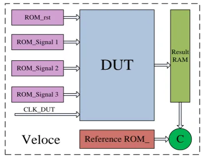
Verification of the design is based on the partition of the software and hardware by the principle mentioned above. In order to reduce the emulation time, the testbench is put into the hardware accelerator directly that makes the system emulation run in hardware entirely. The RISC of the design uses the custom instruction set of ZSP400. According to the instruction set, it proposes the assembler which converts the instruction set to a binary stream automatically. In the verification phase, we select different application scenarios and paths of data flow and control flow as the verification environment, and write the assembly language program at a high transaction-level which can be converted into binary data from the assembler as the test stimulus that are put into the accelerator. Thus, there is no time overhead of the software simulation and the data interaction between hardware and software because of putting the whole testbench into the hardware accelerator directly. At the same time, the result is stored in RAM and compared with the reference data stored in another ROM. The partition structure diagram between software and hardware is illustrated in Fig. 4.
C
DUT
Veloce
ROM_Signal 1
Result RAM
Reference ROM_
ROM_Signal 3 ROM_Signal 2 ROM_rst
CLK_DUT
Figure 4. The partition structure diagram between software and hardware
B. SOC System-Level Verification Scenario Analysis Application scenario for the SOC is extensive. SOC system-level functional verification is relatively complex and time-consuming. In order to ensure the comprehensiveness of verification and satisfy project schedule urgency request, the scenario analysis of SOC system-level verification becomes increasingly important. In this paper, combining with the design characteristics and the project requirements, according to dividing the different application scenarios, the system-level verification method based on the paths of data flow and control flow is proposed. Four paths of data flow and control flow based on different application scenarios are demonstrated in Fig. 5.
① RISC CPU--AXI high-speed bus--Protocol conversion bridge--APB low-speed bus--Peripheral
Interface UART0, UART1, SPI1, GPIO, IIC. This path is used for reading and writing data or transmitting signals to low-speed peripherals with the control of processor core.
② RISC CPU--AXI high-speed bus--SPI0. This pathway is used to read and write data or transmit signals
RISC CPU Core
A
P
B
B
U
S
DMA Control
Bridge JTAG
A
X
I
B
U
S
SPI0 Data Memory
UART0
IIC Timer WTC INTC RTC GPIO
SPI1 UART1
Figure 5. Paths of data flow and control flow in system
to the SPI0 high-speed peripheral interface under the control of processor core.
③ RISC CPU--AXI high-speed bus--Data Memory. This path is used to read and write data or transmit signals to on-chip memory with processor core.
④ Data Memory or SPI0--AXI high-speed bus--Data transmission channel DMA--APB low-speed bus--Peripheral Interface UART0, UART1, SPI1, GPIO, and IIC. This path is used to transfer large and continuous data between Data Memory or an external SPI Flash Memory connected with SPI0 and low-speed Peripheral Interface UART0, UART1, SPI1, GPIO, IIC etc.
C. Memory Mapping and Optimization
Based on the hardware and software partitioning method mentioned above, the whole testbench is put in accelerator. In order to improve the emulation speed, a lot of memories for storing design and test stimulus are needed. So, how to correctly design and optimize the memory model are very important. Designing the memory model requires to consider three aspects of the problem. 1) Whether meet the requirements of sequence and size for the design. 2) Whether can be synthesized. 3) Memory area optimization problem.
D. System Debugging Control
In order to increase the flexibility of the system debugging features and control the emulation process, the trigger state machines driven by state transition conditions are designed. They involve setting the states
module DROM1024X16M8 (CLK,CEN,DOUT, AD); parameter WORD_WIDTH=16;
parameter WORD_DEPTH=1024; parameter ADDR_WIDTH=10; input CLK;
input CEN;
input [ADDR_WIDTH-1:0] AD; output [WORD_WIDTH-1:0] DOUT; reg [WORD_WIDTH-1:0] DOUT;
reg [WORD_WIDTH-1:0] DROM1024X16M8[WORD_DEPTH-1:0]; // pragma attribute DROM1024X16M8 ram_block 1
always @ (posedge CLK) begin
if (!CEN)
DOUT <= DROM1024X16M8[AD]; end
endmodule
Figure 6. DROM model
names, start and end points of tracking data, the state transition conditions, the trigger points of states, the stop points of system and so on. The state machines can control the start and the stop of the system emulation, as well as the emulation tracking data. They also can be used to judge whether the expected states have been reached or not and observe the correctness of the design corresponding the arrivals of the states. The portions of triggers in the system are illustrated in Fig. 7.
S0
s
S1
s
S2
s
soc_veloce.u_soc_top. clk_25mh == 1
soc_veloce.u_soc_top. clk_1kh == 1
soc_veloce.u_soc_top. clK_1h == 1 10 times
S0
s
S1
s
S2
s
soc_veloce.resetdriver.re set == 1
soc_veloce.resetdriver.re set == 0
soc_veloce.u_soc_top.u_ris c_top.u_pipeline_top.u_for warding_logic.gp_reg_13[1 5:0]==16'h0001
S3
d
S3
d
Figure 7. The portions of triggers in the system
V. SIMULATION RESULTS ANALYSIS
To compare the system-level simulation speed and performance of software simulation with those of hardware accelerator, the data path ① and the data path
② are taken for examples.
For the data path ①, the running light program is used as a test case. RISC CPU writes data to the peripherals GPIO and drives LED to lit running lights. The pipelining interval of running lights mainly relies on the control of internal loop counter in RISC. The pipelining interval is larger, the emulation time is longer. During the emulation of the hardware accelerator, the running light program which is described by high transaction-level is converted to the test stimulus from the assembler mentioned above. After that, put it into the DROM of the RISC I_MEM module. Moreover, add the trigger which is designed above. Then, start the emulation. The waveform is given in Fig. 8 at the end of the emulation.
Figure 8. The waveform at the end of the emulation for running lights
For the data path ②, the bubbling program is used as a test case which procedures for the 5000 random numbers of 16 bits according to the order from the small to the large. When the hardware accelerator emulation starts, in addition to import test stimulus and trigger, it also should put 5000 random numbers of hexadecimal into SRAM. At the end of emulation, the part of waveform and the trigger point are shown in Fig. 9 and Fig. 10 respectively.
Figure 9. The waveform at the end of the emulation for bubbling
Figure 10. The log of the trigger
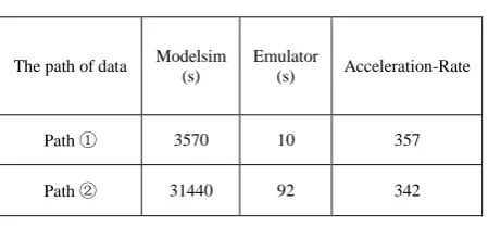
TABLE II. THE COMPARISON OF THE SPEED BETWEEN THE TWO SIMULATION METHODS
The path of data Modelsim (s)
Emulator
(s) Acceleration-Rate
Path ① 3570 10 357
Path ② 31440 92 342
From table II, for the system-level SOC verification, authentication method, mentioned in this article, wins an immense acceleration effect. As illustration in Fig. 8, 9 and 10, with the state machine transitions, the trigger technique has a strong performance in system emulation control and bug tracking.
VI. CONCLUSION
The system-level verification is critical in a SOC design process due to the IP cores passing certification. Directing at complicated applications and various function features, the SOC system-level verification is segmented into comprehensive test scenarios, according to the paths of data flow and control flow. The SW/ HW partition principle with overall hardware verification acquired an immense acceleration effect. The method of trigger-driver-based state transition diagram is adopted in system debugging to control emulation process, which improves the flexibility of debugging and the veracity of tracking on an emulator. The tape out of a DSP chip designed in a 0.18um CMOS process is successful in this method.
ACKNOWLEDGMENT
This work is supported by Science-Technology
Program of Shenzhen, China (Grate
NO.JCYJ20120614150044545). Thanks Teng Wang and Yin-Hui Wang in IMS lab of SZPKU for their discussion and advice on correcting errors at compiling and emulation phases.
REFERENCES
[1] Y. B. Liao, P. Li, A.W. Ruan, Y. W. Wang, W. C. Li, and W. Li, “Hierarchy communication channel in transaction-level hardware/software co-emulation system,” in Proc. Ninth International Workshop on Microprocessor Test and Verification, 2008, pp. 94-99, 8th-10th Dec.,
[2] W. Huang, X. A. Wang, P. Dai, and Z. Guo, “Implementation of high-speed verification platform based on emulator for ReDSP and ReMAP,” in Proc. IEEE 8th International Conference on ASIC, 20-23 Oct. 2009, pp. 682-685,
[3] T. Lins and E. Barros, “The development of a hardware abstraction layer generator for system-on-chip functional verification,” in Proc. 2010 VI Southern Programmable Logic Conference, March 2010, pp.41-46.
[4] S. Banerjee, T. Gupta, and S. Jain, “A scalable hybrid verification system based on HDL slicing,” 2011 IEEE International High
Level Design Validation and Test Workshop, pp. 41-48, 9th-11st Nov. 2011.
[5] Veloce User's Guide, Mentor Graphics, Software Version V1.2.3, 2007.
[6] C. Y. Huang, Y. F. Yin, C. J. Hsu, C. Y. Huang, T. M. Chang, “SOC HW/SW verification and validation,” 2011 16th Asia and South Pacific Design Automation Conference, pp. 297-300, 25th-28th Jan. 2011.
[7] J. Aylward, C. H. Crawford, K. Inoue, S. Lekuch, K. Muller, M. Nutter, H. Penner, K. Schleupen, and J. Xenidis, “Reconfigurable systems and flexible programming for hardware design, verification and software enablement for system-on-a-chip architectures,” in Proc. 2011 International Conference on Reconfigurable Computing and FPGAs, Nov.30th-Dec.2nd, 2011, pp. 351-356.
[8] S. Banerjee and T. Gupta, “Fast and scalable hybrid functional verification and debug with dynamically reconfigurable co-simulation,” in Proc. 2012 IEEE/ACM International Conference on Computer-Aided Design, 5-8 Nov.2012, pp. 115-122. [9] I. Mavroidis and I. Papaefstathiou, “Efficient testbench code
synthesis for a hardware emulator system,” Design, Automation & Test in Europe Conference & Exhibition, pp. 1-6, April.2007. [10] I. Mavroidis, I. Mavroidis, and I. Papaefstathiou, “Accelerating
emulation and providing full chip observability and controllability at run-time,” Design & Test, IEEE, vol. pp. no.99, pp. 1, Mar. 2013.
Shi-Jun Li received the B.S. degree in Electronic information engineering, Yunnan University, Yunnan, China. He is currently working toward the M.S. degree in integrated circuit and system at Peking University. He research interests include digital design and verification on SOC based on hardware accelerator.
Zheng Xie received the B.S. degree from Kunming University of Science and Technology, Kunming, Yunnan, in 2008. He is currently pursuing the Ph.D. degree in school of electronics engineering and computer science, Peking University. He is now engaged in the operator design and verification methodology and verification expert system (VES) at school of electronic and computer engineering, Shenzhen. His current research interests include IC design and verification, computer-aided design tool development.