Tunable Wide-Band Second-Order All-Pass
Filter-Based Time Delay Cell Using Active Inductor
Seyed Rasoul Aghazadeh, Alireza Saberkari
Microelectronics Research Lab.Department of Electronics Engineering, University of Guilan Rasht, Iran
Herminio Martinez, Eduard Alarcon
Department of Electronics EngineeringTechnical University of Catalunya (UPC), BarcelonaTech Barcelona, Spain
{herminio.martinez; eduard.alarcon}@upc.edu
Abstract—This paper presents a CMOS RF second-order voltage-mode all-pass filter (APF) as a time delay cell. The proposed filter benefits from a simple structure; consisting of one transistor, three resistors, and one grounded capacitor and inductor. The filter reaches a group delay of 60 ps over a 10 GHz bandwidth, while achieving maximum delay-bandwidth-product (DBW) and it consumes only 10.3 mW power. On the other hand, an active inductor is used in the APF instead of a passive RLC tank in order to control the time delay and improve the size. In this case, the power consumption increases while time delay can be tuned. The proposed APF is designed and simulated in a TSMC 180 nm CMOS process.
Keywords—all-pass filter; delay; wide-band; delay-bandwidth-product; active inductor
I. INTRODUCTION
All-pass filters (APFs) as delay stages are used for real-ization of delay structures in many different radio frequency (RF) circuits and phase shift applications like synchronizing ultra-wideband (UWB) impulse radios with locally generated reference pulses, equalizers, and analog beamformers [1]−[3]. All-pass-filter-based time delays provide better performance in terms of area-efficiency and loss than alternative methods based on transmission lines or lumped LC delay lines, which are area consuming and impractical for on-chip implemen-tations. Therefore, implementations of wideband analog RF beamformers using all-pass-filter-based delay approximations have recently received attention [4], [5].
In some circuits, the delay stage is usually realized by cascading first-order all-pass gm-(R)C filters. However, these circuit topologies suffer from limited bandwidths around low-GHz (up to 2.5low-GHz) [5], [6]. Generally, high-order rational APFs can be decomposed into several second-order APFs with complex-conjugate poles and first-order APFs. Therefore, a second-order APF is a key component for realization of a delay structure with nanosecond delay. There are several current-and voltage-mode APFs in the literature [7]−[9], most of them use one or more operational voltage or current amplifiers that suffer from low bandwidth due to the presence of high impedance nodes though. These filters are therefore limited to low frequencies of operation.
In this paper, a CMOS wide-band second-order APF using an active inductor to control time delay is proposed. The proposed circuit employs pad´e approximation, which provides
the best approximation of an ideal delay; because it achieves flatter group delay over a larger bandwidth than any other approximation [10], [11]. For achieving maximum delay-bandwidth-product (DBW), second-order APFs using Pad´e technique are better selections than the cascade of two first-order APFs to realize a second-first-order delay structure.
The structure of this paper is as follows. In Section II, the proposed APF is designed and analyzed. Section III presents the tunability of the proposed second-order APF. The results are given in Section IV and finally, Section V provides conclusions.
II. PROPOSEDSECOND-ORDERAPF
The ideal transfer function of a second-order APF utilizing Pad´e approximation is as follows:
H(s) = s 2−ωn Qs+ω 2 n s2+ωn Qs+ω2n (1) where ωn is the natural frequency of the APF and Q is
the quality factor, which determines the position of poles and zeros in the complex plane. Fig. 1 shows the proposed CMOS second-order APF as a time delay cell. If we neglect the parasitics of the transistors, the transfer function of the proposed second-order APF is defined as below:
Vout Vin(s) =− RL(gm1R1−1) RL+R1 · s2−1 C gm1 +gm2 −gm1gm2R1 gm1R1−1 s+ 1 LC s2+1 C(gm1+gm2)s+LC1 (2) wheregm1andgm2are the transconductances ofM1andM2,
respectively. In order to have an all-pass structure, we must have the DC gain equal to unity and the same coefficients for sin the nominator and denominator of (2), which yields to the following conditions: R1= 2 gm1 (3a) RL R1 (3b) gm1+gm2gm1gm2R1. (3c)
As a result, the transfer function in (2) can be rewritten as below: Vout Vin (s)∼=−s 2− 1 C(gm1+gm2)s+ 1 LC s2+ 1 C(gm1+gm2)s+ 1 LC . (4) 978-1-5386-5108-7/17/$31.00 c2017 IEEE
Fig. 1. The proposed second-order all-pass filter.
Therefore, natural frequency and quality factor of the proposed second-order APF become, respectively, as follows:
ωn= 1 √ LC (5) Q= 1 gm1+gm2 r C L. (6)
Given that transconductancesgm1,2 only affect the quality
factor, the circuit bandwidth and quality factor can be set, inde-pendently. The pole/zero frequencies, phase, and group delay responses of the second-order APF are given, respectively, as below: |ωp1,2|=|ωz1,2|= L(gm1+gm2)± p L2(g m1+gm2)2−4LC 2LC (7) ϕ(ω) =−2tan−1 L(gm1+gm2)· ω 1−LCω2 (8) τg(ω) =− ∂ϕ(ω) ∂ω =2L(gm1+gm2)· 1 +LCω2 (1−LCω2)2+ ((g m1+gm2)Lω) 2. (9) The group delay is2L(gm1+gm2)at DC. WhenQ <0.5,
the APF has two real poles in the left-half plane, while for Q > 0.5 a complex conjugate pole-pair appears. When Q= 1/√3, the maximum flat delay will be achieved and Pad´e approximation is matched. Therefore, the maximum delay-bandwidth-product (DBW) will be guaranteed. Note that, the circuit can achieve larger delay over a wider bandwidth by choosing gm, L, and C appropriately (low transconductance
and small values ofLandC) compared to the gm-(R)C filters, as the natural frequency of the proposed circuit is1/√LC.
In order to consider the effects of parasitic capacitors on the performance of the proposed APF, the effect of Cgd is
neglected due to the fact that its impedance is more thanR1at
high frequencies, corresponding to a very high frequency pole which does not affect the performance of the APF. Therefore,
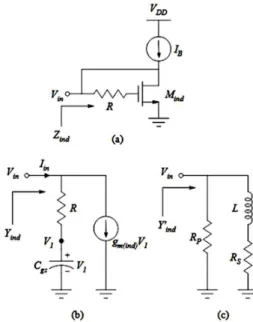
Fig. 2. (a) Active inductor and, (b) and (c) its equivalent models.
Cgs is just assessed for the evaluation. Considering finite
output impedance ofM1and theCgswhich affect the pole/zero
frequency and DC-gain, the transfer function of the second-order APF is as follows:
Vout Vin (s) =−CRL(gm1R1−1)−CgsRL(1 +R1gds) (C+Cgs)(R1+RL+gdsR1RL) · s2−h(gm1+gm2+gds)(1+R1gds)−(gm2+gds)(R1(gm1+gds)) C(gm1R1−1)−Cgs(1+R1gds) i s+ gm1R1−1 LC(gm1R1−1)−LCgs(1+R1gds) s2+h(gm1+gm2+gds)(R1+RL)+gm2gdsR1RL (C+Cgs)(R1+RL+gdsR1RL) i s+ 1 L(C+Cgs) (10) wheregds is the output conductance of M1. Ifgm1,2 gds
and the conditions in (3) are satisfied, the transfer function can be rewritten as below: Vout Vin (s)∼=−C−Cgs C+Cgs ·s 2−gm1+gm2 C−Cgs s+ 1 L(C−Cgs) s2+gm1+gm2 C+Cgs s+ 1 L(C+Cgs) . (11)
As it can be seen, for C Cgs, (4) and (11) will be the
same. Further analysis shows thatCgsmakes variations on the
gain and group delay responses at high frequencies. However, these variations can be adjusted by varying resistorR2 in the
proposed APF, which is assessed in Section IV.
III. THETUNABILITYOFTHEPROPOSED
SECOND-ORDERAPF
In order to control time delay in the proposed second-order APF, active inductors are good options as they offer a variety of advantages; e.g. small area, large and tunable inductance value and self-resonant frequency, and also compatibility with standard CMOS technology [12]. Fig. 2(a) shows a one-port grounded active inductor [13], [14], which is used in the proposed second-order APF. Assuming for simplicity that gm(ind)gds(ind), the input admittance of the active inductor,
Yind(= 1/Zind), can be easily obtained by using its small
Yind= sCgs+gm(ind) sRCgs+ 1 = 1 R + 1 s R2Cgs Rgm(ind)−1+ R Rgm(ind)−1 (12) where pole and zero frequencies of the input admittance of the active inductor are ωp=gm(ind)/Cgs andωz = 1/RCgs,
respectively. The circuit has an inductive behavior in the frequency range ofωz< ω < ωp.
The obtained input admittance in (12) can now be modeled by a parallelRLcircuit shown in Fig. 2(c) as below:
Yind0 =GP+
1
sL+RS
(13) whereGP = 1/RP is determined as parallel andRS as series
resistance with inductorL. From (12) and (13), the parameters of theRLequivalent circuit can be given as:
RP =R (14a) L= R 2C gs Rgm(ind)−1 (14b) RS = R Rgm(ind)−1 . (14c)
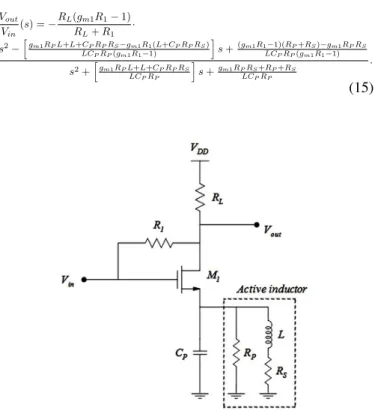
The circuit shown in Fig. 3 is designed to tune the delay of the proposed second-order APF. In this circuit, active inductor shown in Fig. 2(a) is replaced with parallel RLC circuit in Fig. 1. The value of resistor RS is very small and
therefore it can be neglected. CapacitorCP is the total parasitic
capacitances at the source terminal of the transistor M1, and
hence, there is no need to any additional capacitor at this node resulting in a smaller area. The transfer function of the proposed circuit in Fig. 3 is as follows:
Vout Vin (s) =−RL(gm1R1−1) RL+R1 · s2−hgm1RPL+L+CPRPRS−gm1R1(L+CPRPRS) LCPRP(gm1R1−1) i s+(gm1R1−1)(RP+RS)−gm1RPRS LCPRP(gm1R1−1) s2+hgm1RPL+L+CPRPRS LCPRP i s+gm1RPRS+RP+RS LCPRP . (15)
Fig. 3. The proposed second-order all-pass filter using an active inductor.
If gm1RP 1,gm1RS 1, and conditions in (3a)-(3b)
are satisfied, the transfer function can be rewritten as below: Vout Vin (s)∼=−s 2−(gm1 CP)s+ 1 LCP s2+ (gm1 CP)s+ 1 LCP (16) which is nearly the same as that in (4).
IV. RESULTS
The proposed second-order APF is designed in 180nm TSMC CMOS process and the results are obtained from HSPICE simulation with the supply voltage of1.8V. First, the proposed circuit shown in Fig. 1 is simulated with gm1 =
31.5mA/V, gm2 = 3.7mA/V, RL = 3KΩ, R1 = 65Ω, and
Q = 1/√3 (for maximum DBW). In addition, the values of capacitor and inductor are selected as 210fF and 0.85nH, respectively.
In Fig. 4 the gain and phase responses of the second-order APF are shown. The gain roll-off is due to the existence of parasitic effects of the transistors. The group delay response of the proposed APF is shown in Fig. 5, indicating a flat group delay equal to 59.8ps over 10GHz bandwidth, which is very close to the theoretical value in (9). Fig. 6 shows the gain and group delay responses of the second-order APF for different values of R2(= 1/gm2). It is obvious that by varying gm2,
Fig. 4. Gain and phase responses of the proposed second-order all-pass filter.
Fig. 6. Gain and group delay responses of the proposed second-order all-pass filter with different values ofR2= 1/gm2.
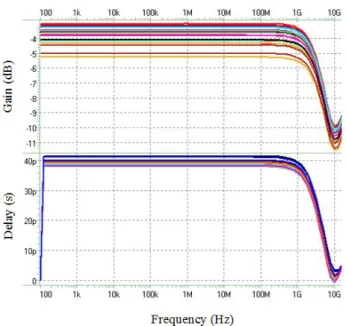
Fig. 7. Gain and group delay responses of the proposed second-order all-pass filter with active inductor for different values ofRP (50−850Ω).
flat gain and group delay responses are achieved at higher frequencies.
Table I indicates the performance comparison of the pro-posed second-order all-pass filter and some other reported wide-band second-order ones. As it can be seen, power con-sumption of the proposed APF is lower than the others. Fur-thermore, the proposed circuit demonstrates a larger bandwidth than the other second-order APFs having the same mode with the exception of the filter in [10] where two inductors were used, resulting in a larger area.
Finally, the proposed second-order APF using an active inductor shown in Fig. 3 is evaluated with gm1 = 18mA/V,
Fig. 8. Monte Carlo simulation results for gain and group delay responses of the proposed second-order all-pass filter with active inductor.
Fig. 9. Corner analysis results for group delay response of the proposed second-order all-pass filter with active inductor.
gm(ind) = 118mA/V, RL = 3KΩ, R1 = 115Ω, and RP =
450Ω. In this case, an inductance ofL= 1.48nH with RS =
8.6Ωis obtained, while the overall active inductor-based APF consumes 33.6mW power from a 1.8V supply voltage. The gain and group delay responses of the proposed APF are shown in Fig. 7. As it can be seen, the delay can be controlled over the frequency band by varying the resistor RP in the active
inductor. Tuning action can be easily performed by a binary weighted resistor bank instead ofR(=RP)in Fig. 2(a).
For further analysis, Monte Carlo and corner analyses are considered and the results are shown in Figs. 8 and 9 respectively, with RP = 250Ω. The Monte Carlo simulation
TABLE I. PERFORMANCECOMPARISONOFTHEPROPOSED
WIDE-BANDSECOND-ORDERALL-PASSFILTERANDOTHERWORKS.
ofM1in Fig. 3, with a Gaussian distribution and50iterations.
In this case, maximum variation on the group delay response of the proposed APF over the frequency band is9.5%.
V. CONCLUSION
This paper has presented a tunable wide-band second-order all-pass filter as a time delay cell. The proposed voltage-mode all-pass filter shows a flat group delay of 60ps over a bandwidth of 10GHz, achieving maximum delay-bandwidth-product (DBW). This filter consumes only 10.3mW and reaches a larger delay across the frequency band than other published second-order voltage-mode APFs using just one grounded inductor. Additionally, an active inductor is utilized in order to control the time delay of the proposed second-order APF and to decrease size. In this condition, the proposed filter consumes around 33.5 mW power, while its time delay is varied for different values of tunable resistor in the active inductor.
ACKNOWLEDGMENT
This work has been partially funded by the Spanish Min-istry of Science and Innovation (project DPI2013-47799- C2-2-R).
REFERENCES
[1] J. Schwartz, I. Arnedo, M. Laso, T. Lopetegi, J. Azana, and D. Plant, “An electronic UWB continuously tunable time-delay system with nanosecond delays,” IEEE Microw. Wireless Compon. Lett., vol. 18, no. 2, pp. 103-105, Feb. 2008.
[2] J. Buckwalter and A. Hajimiri, “An active analog delay and the delay reference loop,” in Proc. IEEE RFIC Symp. (RFIC04), Dig., Jun. 2004, pp. 17-20.
[3] G. Gurun, J. S. Zahorian, A. Sisman, M. Karaman, P. E. Hasler, and F. L. Degertekin, “An analog integrated circuit beamformer for high frequency medical ultrasound imaging,” IEEE Trans. Biomedical Circuits Syst., vol. 6, no. 5, pp. 454-467, Oct. 2012.
[4] C. Wijenayake, Y. Xu, A. Madanayake, L. Belostotski, and L. Bruton, “RF analog beamforming fan filters using CMOS all-pass time delay approximations,” IEEE Trans. Circuits Syst. I, vol. 59, no. 5, pp. 1061-1073, May 2012.
[5] S. K. Garakoui, E. A. M. Klumperink, B. Nauta, and F. E. van Vliet, “Compact cascadable gm-C all-pass true time delay cell with reduced delay variation over frequency,” IEEE J. Solid-State Circuits, vol. 50, no. 3, pp. 693-703, Mar. 2015.
[6] S. K. Garakoui, E. A. M. Klumperink, B. Nauta, and F. E. van Vliet, “Frequency limitations of first-order gm-RC all-pass delay circuits,” IEEE Trans. Circuits Syst. II, vol. 60, no. 9, pp. 572-576, Aug. 2013. [7] A. Toker, S. Ozoguz, O. Cicekoglu, and C. Acar, “Current-mode allpass
filters using current differencing buffered amplifier and a new high-Q bandpass filter configuration,” IEEE Trans. Circuits Syst. II, vol. 47, no. 9, pp. 949-954, Sept. 2000.
[8] C. Cakir, U. Cam, and O. Cicekoglu, “Novel allpass filter configuration employing single OTRA,” IEEE Trans. Circuits Syst. II, vol. 52, no. 3, pp. 122-125, Mar. 2005.
[9] C. M. Chang, “Current mode allpass/notch and bandpass filter using single CCII,” Electron. Lett., 27, no. 20, pp. 1812-1813, Sept. 1991. [10] L. Zhou, A. Safarian, and P. Heydari, “CMOS wideband analogue delay
stage,” Electron. Lett., vol. 42, no. 21, pp. 1213-1214, Oct. 2006. [11] P. Ahmadi, M. H. Taghavi, L. Belostotski, and A. Madanayake,
“10-GHz current-mode 1st-and 2nd-order allpass filters on 130nm CMOS,” in Proc. IEEE Int. Midwest Symp. Circuits Syst. (MWSCAS13), Aug. 2013, pp. 1-4.
[12] A. Saberkari, S. Ziabakhsh, H. Martinez, and E. Alarcon, “Active inductor-based tunable impedance matching network for RF power amplifier application,” Integration, the VLSI J., vol. 52, pp. 301-308, Jan. 2016.
[13] F. Carreto-Castro, J. Silva-Martinez, and R. Murphy-Arteaga, “RF low-noise amplifiers in BiCMOS technologies,” IEEE Trans. Circuits Syst. II, vol. 46, no. 7, pp. 974-977, Jul. 1999.
[14] A. Saberkari, Sh. Kazemi, V. Shirmohammadli, and M.C.E. Yagoub, “Gm-boosted flat gain UWB low noise amplifier with active inductor-based input matching network,” Integration, the VLSI J., vol. 52, pp. 323-333, Jan. 2016.
[15] A. Ulusoy, B. Schleicher, and H. Schumacher, “A tunable differential all-pass filter for uwb true time delay and phase shift applications,” IEEE Microw. Wireless Compon. Lett., vol. 21, no. 9, pp. 462-464, Sept. 2011.
[16] P. Ahmadi, B. Maundy, A. S. Elwakil, L. Belostotski, and A. Madanayake, “A new 2nd-order all-pass filter in 130-nm CMOS,” IEEE Trans. Circuits Syst. II: Express Briefs, vol. 63, no. 3, pp. 249-253, Mar. 2016.