/ LMV358 /
LMV324
— General-Purpose,
Lo
w V
o
lt
age,
Rail-to-Ra
il Output
Amplifiers
Frequency Response vs. CL Magnitude (1dB/div) Frequency (MHz) 0.01 0.1 1 10 CL = 200pF Rs = 0 CL = 20pF Rs = 0 CL = 200pF Rs = 225Ω CL = 100pF Rs = 0 CL = 10pF Rs = 0 CL = 2pF Rs = 0 CL = 50pF Rs = 0 + -10kΩ 10kΩ Rs CL 2kΩLMV321 / LMV358 / LMV324
General-Purpose, Low Voltage, Rail-to-Rail Output
Amplifiers
Features at +2.7V
• 80 μA Supply Current per Channel • 1.2 MHz Gain Bandwidth Product • Output Voltage Range: 0.01 V to 2.69 V • Input Voltage Range: -0.25 V to +1.5 V • 1.5 V/μs Slew Rate
• LMV321 Directly Replaces Other Industry Standard LMV321 Amplifiers: Available in SC70-5 and SOT23-5 Packages
• LMV358 Directly Replaces Other Industry Standard LMV358 Amplifiers: Available in MSOP-8 and SOIC-8 Packages
• LMV324 Directly Replaces Other Industry Standard LMV324 Amplifiers: Available in SOIC-14 Packages • Fully Specified at +2.7 V and +5 V Supplies • Operating Temperature Range: -40°C to +125°C
Applications
• Low Cost General-Purpose Applications • Cellular Phones
• Personal Data Assistants • A/D Buffer
• DSP Interface • Smart Card Readers • Portable Test Instruments • Keyless Entry
• Infrared Receivers for Remote Controls • Telephone Systems
• Audio Applications • Digital Still Cameras • Hard Disk Drives
Description
The LMV321 (single), LMV358 (dual), and LMV324 (quad) are a low cost, voltage feedback amplifiers that consume only 80 μA of supply current per amplifier. The LMV3XX family is designed to operate from 2.7 V (±1.35 V) to 5.5 V (±2.75 V) supplies. The common mode volt-age range extends below the negative rail and the output provides rail-to-rail performance.
The LMV3XX family is designed on a CMOS process and provides 1.2 MHz of bandwidth and 1.5 V/μs of slew rate at a low supply voltage of 2.7 V. The combination of low power, rail-to-rail performance, low voltage opera-tion, and tiny pack-age options make the LMV3XX family well suited for use in personal electronics equipment such as cellular handsets, pagers, PDAs, and other bat-tery powered applications.
Typical Application
6.8μF +Vs
/ LMV358 /
LMV324
— General-Purpose,
Lo
w V
o
lt
age,
Rail-to-Ra
il Output
Amplifiers
Ordering Information
Pin Assignments
LMV321
LMV358
LMV324
Product Number Package Packing Method Operating Temperature
LMV321AP5X SC70 5L Tape and Reel, 3000pcs
-40 to +125°C
LMV321AS5X SOT-23 5L Tape and Reel, 3000pcs
LMV358AM8X SOIC 8L (Narrow) Tape and Reel, 2500pcs
LMV358AMU8X MSOP 8L Tape and Reel, 3000pcs
LMV324AM14X SOIC 14L Tape and Reel, 2500pcs
– + 1 2 3 +In -Vs -In +Vs Out 5 4 – + 1 2 3 +In -Vs -In +Vs Out 5 4 SC70-5 SOT23-5 -+ -+ 1 2 3 4 Out1 -In1 +In1 -Vs +Vs Out2 -In2 +In2 8 7 6 5 MSOP-8 -+ -+ 1 2 3 4 Out1 -In1 +In1 -Vs +Vs Out2 -In2 +In2 8 7 6 5 SOIC-8 1 2 3 4 Out1 -In1 +In1 +Vs Out4 -In4 +In4 -Vs 14 13 12 11 5 6 7 +In2 -In2 Out2 +In3 -In3 Out3 10 9 8 -+ -+ -+ -+ SOIC-14
/ LMV358 /
LMV324
— General-Purpose,
Lo
w V
o
lt
age,
Rail-to-Ra
il Output
Amplifiers
Absolute Maximum Ratings
Stresses exceeding the absolute maximum ratings may damage the device. The device may not function or be opera-ble above the recommended operating conditions and stressing the parts to these levels is not recommended. In addi-tion, extended exposure to stresses above the recommended operating conditions may affect device reliability. The absolute maximum ratings are stress ratings only.
Recommended Operating Conditions
Package Thermal Resistance
Parameter Min. Max. Unit
Supply Voltage 0 +6 V
Maximum Junction Temperature - +175 °C
Storage Temperature Range -65 +150 °C
Lead Temperature, 10 Seconds - +260 °C
Input Voltage Range -VS -0.5 +VS +0.5 V
Parameter Min. Max. Unit
Operating Temperature Range -40 +125 °C
Power Supply Operating Range 2.5 5.5 V
Package θJA Unit 5 Lead SC70 331.4 °C/W 5 Lead SOT23 256 °C/W 8 Lead SOIC 152 °C/W 8 Lead MSOP 206 °C/W 14 Lead SOIC 88 °C/W
/ LMV358 /
LMV324
— General-Purpose,
Lo
w V
o
lt
age,
Rail-to-Ra
il Output
Amplifiers
Electrical Specifications
TC = 25°C, VS = +2.7 V, G = 2, RL = 10 kΩ to VS/2, Rf = 10 kΩ, VO(DC) = VCC/2, unless otherwise noted.
Min/max ratings are based on product characterization and simulation. Individual parameters are tested as noted. Outgoing quality levels are determined from tested parameters.
Notes:
1. Guaranteed by testing or statistical analysis at +25°C.
2. +IN and -IN are gates to CMOS transistors with typical input bias current of <1 nA. CMOS leakage is too small to practically measure.
Parameter Conditions Min. Typ. Max. Unit AC Performance
Gain Bandwidth Product CL= 50 pF, RL= 2 kΩ to VS/2 1.2 MHz
Phase Margin 52 deg
Gain Margin 17 dB
Slew Rate VO = 1VPP 1.5 V/μs
Input Voltage Noise >50 kHz 36 nV/√Hz
Crosstalk LMV358 100 kHz 91 dB
LMV324 100 kHz 80
DC Performance
Input Offset Voltage(1) 1.7 7.0 mV
Average Drift 8 μV/°C
Input Bias Current(2) <1 nA
Input Offset Current(2) <1 nA
Power Supply Rejection Ratio(1) DC 50 65 dB
Supply Current (Per Channel)(1) 80 120 μA
Input Characteristics
Input Common Mode Voltage Range(1) LO 0 -0.25 V
HI 1.5 1.3
Common Mode Rejection Ratio(1) 50 70 dB
Output Characteristics
Output Voltage Swing RL= 10 kΩ to VS/2; LO
(1) 0.01 0.10
V RL= 10 kΩ to VS/2; HI(1) 2.60 2.69
/ LMV358 /
LMV324
— General-Purpose,
Lo
w V
o
lt
age,
Rail-to-Ra
il Output
Amplifiers
Electrical Specifications (Continued)
TC = 25°C, VS = +5 V, G = 2, RL = 10 kΩ to VS/2, Rf = 10 kΩ, VO(DC) = VCC/2, unless otherwise noted.
Min/max ratings are based on product characterization and simulation. Individual parameters are tested as noted. Outgoing quality levels are determined from tested parameters.
Notes:
3. Guaranteed by testing or statistical analysis at +25°C.
4. +IN and -IN are gates to CMOS transistors with typical input bias current of <1 nA. CMOS leakage is too small to practically measure.
Parameter Conditions Min. Typ. Max. Unit AC Performance
Gain Bandwidth Product CL= 50 pF, RL= 2 kΩ to VS/2 1.4 MHz
Phase Margin 73 deg
Gain Margin 12 dB
Slew Rate 1.5 V/μs
Input Voltage Noise >50 kHz 33 nV/√Hz
Crosstalk LMV358 100 kHz 91 dB
LMV324 100 kHz 80 dB
DC Performance
Input Offset Voltage(3) 1 7 mV
Average Drift 6 μV/°C
Input Bias Current(4) <1 nA
Input Offset Current(4) <1 nA
Power Supply Rejection Ratio(3) DC 50 65 dB
Open Loop Gain(3) 50 70 dB
Supply Current (Per Channel)(3) 100 150 μA
Input Characteristics
Input Common Mode Voltage Range(3) LO 0 -0.4 V
HI 3.8 3.6 V
Common Mode Rejection Ratio(3) 50 75 dB
Output Characteristics
Output Voltage Swing
RL= 2 kΩ to VS/2; LO/HI 0.036 to
4.950 V
RL= 10 kΩ to VS/2; LO(3) 0.013 0.100 V
RL= 10 kΩ to VS/2; HI(3) 4.90 4.98 V
Short Circuit Output Current(3) Sourcing; VO = 0 V 5 +34 mA
/ LMV358 /
LMV324
— General-Purpose,
Lo
w V
o
lt
age,
Rail-to-Ra
il Output
Amplifiers
Typical Operating Characteristics
TC = 25°C, VS = +5 V, G = 2, RL = 10 kΩ to VS/2, Rf = 10 kΩ, VO(DC) = VCC/2, unless otherwise noted. Non-Inverting Freq. Response Vs = +5V
Normalized Magnitude (1dB/div)
Frequency (MHz) 0.01 0.1 G = 10 1 10 G = 5 G = 1 G = 2
Inverting Frequency Response Vs = +5V
Normalized Magnitude (1dB/div)
Frequency (MHz) 0.01 0.1 G = -10 1 10 G = -5 G = -1 G = -2
Non-Inverting Freq. Response Vs = +2.7V
Normalized Magnitude (1dB/div)
Frequency (MHz) 0.01 0.1 G = 10 1 10 G = 5 G = 1 G = 2
Inverting Freq. Response Vs = +2.7V
Normalized Magnitude (1dB/div)
Frequency (MHz) 0.01 0.1 G = -10 1 10 G = -5 G = -1 G = -2 Frequency Response vs. CL Magnitude (1dB/div) Frequency (MHz) 0.01 0.1 1 10 CL = 200pF Rs = 0 CL = 20pF Rs = 0 CL = 200pF Rs = 225Ω CL = 100pF Rs = 0 CL = 10pF Rs = 0 CL = 2pF Rs = 0 CL = 50pF Rs = 0 + -10kΩ 10kΩ Rs CL 2kΩ Frequency Response vs. RL Magnitude (1dB/div) Frequency (MHz) 0.01 0.1 1 10 RL = 1kΩ RL = 2kΩ RL = 100kΩ RL = 10kΩ
Small Signal Pulse Response
Output (V) Time (μs) 0 2 4 6 8 10 12 14 16 18 20 -0.05 0.1 0.25 0 0.05 0.2 0.15
Large Signal Pulse Response
Output (V) Time (μs) 0 2 4 6 8 10 12 14 16 18 20 -0.5 0.1 2.5 0 0.5 2 1.5
/ LMV358 /
LMV324
— General-Purpose,
Lo
w V
o
lt
age,
Rail-to-Ra
il Output
Amplifiers
Typical Operating Characteristics (Continued)
TC = 25°C, VS = +5 V, G = 2, RL = 10 kΩ to VS/2, Rf = 10 kΩ, VO(DC) = VCC/2, unless otherwise noted. Input Voltage Noise
nV/ √ Hz Frequency (kHz) 1 10 100 1000 20 30 40 50 60 70 80 100
Total Harmonic Distortion
THD (%) Frequency (kHz) 0.1 1 10 100 0 0.1 0.2 0.3 0.4 0.5 0.6 Vo = 1Vpp
Open Loop Gain & Phase vs. Frequency
Open Loop Phase (deg)
Frequency (Hz) 10M 10 100 1k 10k 100k 1M -270 -225 -180 0 -135 -45 -90 -20 0 20 100 40 80 60
Open Loop Gain (dB)
|Gain| Phase
RL= 2kΩ
/ LMV358 /
LMV324
— General-Purpose,
Lo
w V
o
lt
age,
Rail-to-Ra
il Output
Amplifiers
Application Information
General DescriptionThe LMV3XX family are single supply, general-purpose, voltage-feedback amplifiers that are pin-for-pin compati-ble and drop in replacements with other industry standard LMV321, LMV358, and LMV324 amplifiers. The LMV3XX family is fabricated on a CMOS process, features a rail-to-rail output, and is unity gain stable.
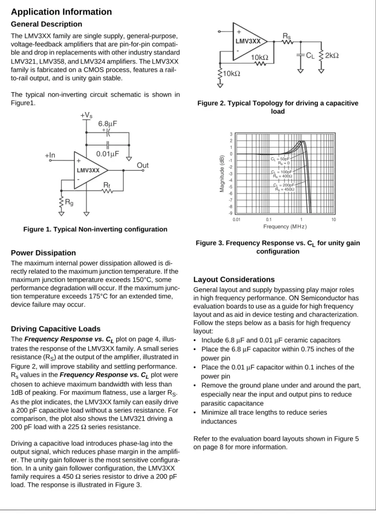
The typical non-inverting circuit schematic is shown in Figure1.
Figure 1. Typical Non-inverting configuration
Power Dissipation
The maximum internal power dissipation allowed is di-rectly related to the maximum junction temperature. If the maximum junction temperature exceeds 150°C, some performance degradation will occur. If the maximum junc-tion temperature exceeds 175°C for an extended time, device failure may occur.
Driving Capacitive Loads
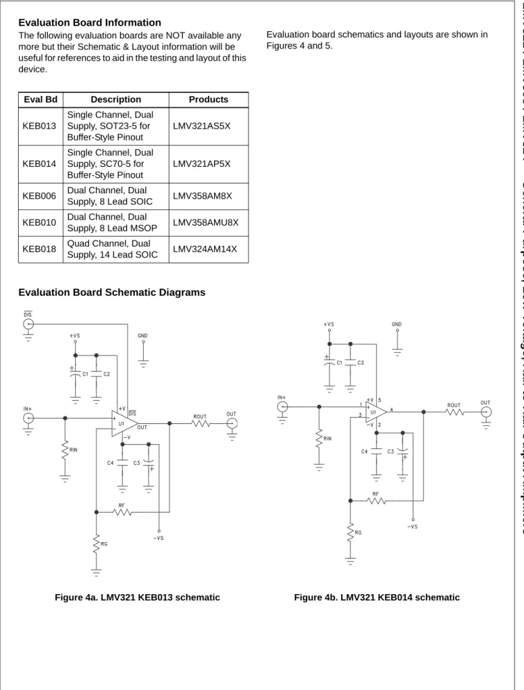
The Frequency Response vs. CL plot on page 4, illus-trates the response of the LMV3XX family. A small series resistance (RS) at the output of the amplifier, illustrated in Figure 2, will improve stability and settling performance. Rs values in the Frequency Response vs. CL plot were chosen to achieve maximum bandwidth with less than 1dB of peaking. For maximum flatness, use a larger RS. As the plot indicates, the LMV3XX family can easily drive a 200 pF capacitive load without a series resistance. For comparison, the plot also shows the LMV321 driving a 200 pF load with a 225 Ω series resistance.
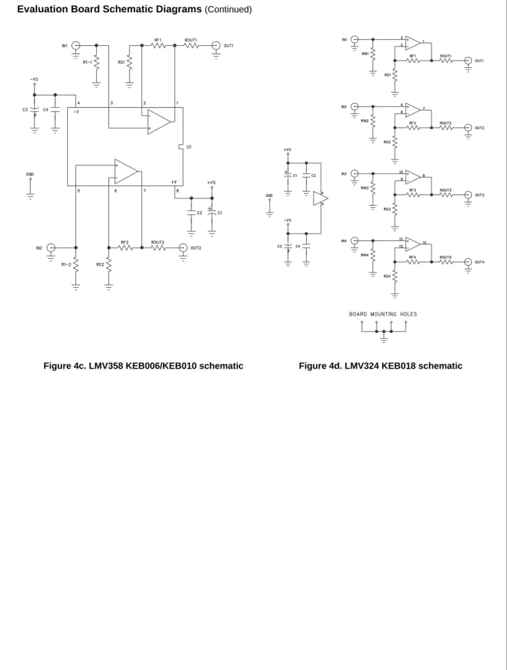
Driving a capacitive load introduces phase-lag into the output signal, which reduces phase margin in the amplifi-er. The unity gain follower is the most sensitive configura-tion. In a unity gain follower configuration, the LMV3XX family requires a 450 Ω series resistor to drive a 200 pF load. The response is illustrated in Figure 3.
Figure 2. Typical Topology for driving a capacitive load
Figure 3. Frequency Response vs. CL for unity gain configuration
Layout Considerations
General layout and supply bypassing play major roles in high frequency performance. ON Semiconductor has evaluation boards to use as a guide for high frequency layout and as aid in device testing and characterization. Follow the steps below as a basis for high frequency layout:
• Include 6.8 μF and 0.01 μF ceramic capacitors • Place the 6.8 μF capacitor within 0.75 inches of the
power pin
• Place the 0.01 μF capacitor within 0.1 inches of the power pin
• Remove the ground plane under and around the part, especially near the input and output pins to reduce parasitic capacitance
• Minimize all trace lengths to reduce series inductances
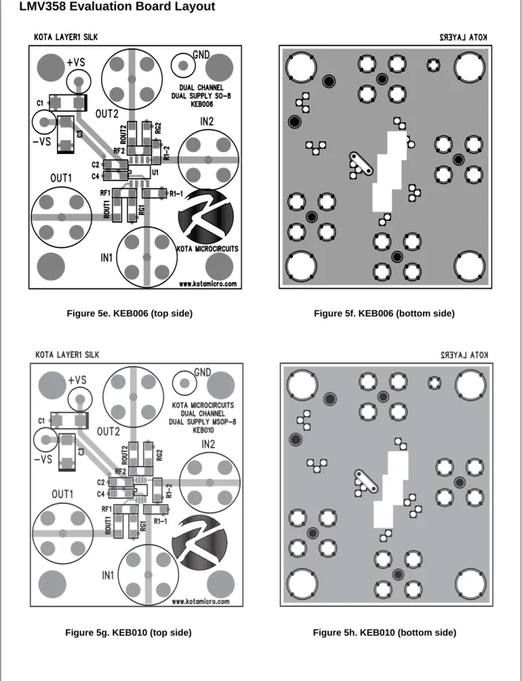
Refer to the evaluation board layouts shown in Figure 5 on page 8 for more information.
+ -LMV3XX Rf 0.01μF 6.8μF Out +In +Vs + Rg + -10kΩ 10kΩ Rs CL 2kΩ LMV3XX Magnitude (dB) Frequency (M H z ) 0.01 0.1 1 10 -9 -8 -7 -6 -5 -4 -3 -2 -1 0 1 2 3 CL= 50pF Rs= 0 CL= 100pF Rs= 400Ω CL= 200pF Rs= 450Ω
/ LMV358 /
LMV324
— General-Purpose,
Lo
w V
o
lt
age,
Rail-to-Ra
il Output
Amplifiers
Evaluation Board Schematic Diagrams
Figure 4a. LMV321 KEB013 schematic Figure 4b. LMV321 KEB014 schematic
Evaluation Board Information
The following evaluation boards are NOT available any more but their Schematic & Layout information will be useful for references to aid in the testing and layout of this device.
Evaluation board schematics and layouts are shown in Figures 4 and 5.
Eval Bd Description Products
KEB013
Single Channel, Dual Supply, SOT23-5 for Buffer-Style Pinout
LMV321AS5X
KEB014
Single Channel, Dual Supply, SC70-5 for Buffer-Style Pinout
LMV321AP5X
KEB006 Dual Channel, Dual
Supply, 8 Lead SOIC LMV358AM8X KEB010 Dual Channel, Dual
Supply, 8 Lead MSOP LMV358AMU8X KEB018 Quad Channel, Dual
/ LMV358 /
LMV324
— General-Purpose,
Lo
w V
o
lt
age,
Rail-to-Ra
il Output
Amplifiers
Evaluation Board Schematic Diagrams (Continued)
/ LMV358 /
LMV324
— General-Purpose,
Lo
w V
o
lt
age,
Rail-to-Ra
il Output
Amplifiers
LMV321 Evaluation Board Layout
Figure 5a. KEB013 (top side) Figure 5b. KEB013 (bottom side)
/ LMV358 /
LMV324
— General-Purpose,
Lo
w V
o
lt
age,
Rail-to-Ra
il Output
Amplifiers
LMV358 Evaluation Board Layout
Figure 5e. KEB006 (top side) Figure 5f. KEB006 (bottom side)
/ LMV358 /
LMV324
— General-Purpose,
Lo
w V
o
lt
age,
Rail-to-Ra
il Output
Amplifiers
LMV324 Evaluation Board Layout
/ LMV358 /
LMV324
— General-Purpose,
Lo
w V
o
lt
age,
Rail-to-Ra
il Output
Amplifiers
Physical Dimensions
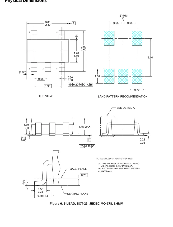
Figure 6. 5-LEAD, SOT-23, JEDEC MO-178, 1.6MM 5
1
4
3 2
LAND PATTERN RECOMMENDATION B A L C 0.10 C 0.20 C A B 0.60 REF 0.55 0.35 SEATING PLANE 0.25 GAGE PLANE 8° 0°
NOTES: UNLESS OTHEWISE SPECIFIED
A) THIS PACKAGE CONFORMS TO JEDEC MO-178, ISSUE B, VARIATION AA, B) ALL DIMENSIONS ARE IN MILLIMETERS. 1.45 MAX 1.30 0.90 0.15 0.05 1.90 0.95 0.500.30 3.00 2.60 1.70 1.50 3.00 2.80 SYMM C 0.95 0.95 2.60 0.70 1.00 SEE DETAIL A 0.22 0.08 C) MA05Brev5 TOP VIEW (0.30)
/ LMV358 /
LMV324
— General-Purpose,
Lo
w V
o
lt
age,
Rail-to-Ra
il Output
Amplifiers
/ LMV358 /
LMV324
— General-Purpose,
Lo
w V
o
lt
age,
Rail-to-Ra
il Output
Amplifiers
Physical Dimensions (Continued)
/ LMV358 /
LMV324
— General-Purpose,
Lo
w V
o
lt
age,
Rail-to-Ra
il Output
Amplifiers
Physical Dimensions (Continued)
Figure 9. 8-LEAD, MSOP, JEDEC MO-187, 3.0MM WIDE
0.45 0.65 1.30 MIN 0.65 4.20 5.50 3.00±0.10 3.00±0.10 4.90±0.15 0.34 PIN #1 ID QUADRANT A B 1.10 MAX 0.15 0.05 0.65 0.38 0.27 0.10M A B C C 0.230.13 A 12°
TOP & BOTTOM
0.95 0.25 0°-8 0.70 0.40 DETAIL A SCALE 20 : 1 GAUGE PLANE SEATING PLANE NOTES: UNLESS OTHERWISE SPECIFIED
A. THIS PACKAGE CONFORMS TO JEDEC MO-187. B. ALL DIMENSIONS ARE IN MILLIMETERS. C. DIMENSIONS ARE EXCLUSIVE OF BURRS,
MOLD FLASH AND TIE BAR EXTRUSIONS. D. DIMENSIONS AND TOLERANCES AS PER ASME
Y14.5-1994.
E. LAND PATTERN AS PER IPC7351#TSOP65P490X110-8BL F. FILE NAME: MKT-MUA08AREV4
4 1
LAND PATTERN RECOMMENDATION TOP VIEW
SIDE VIEW
/ LMV358 /
LMV324
— General-Purpose,
Lo
w V
o
lt
age,
Rail-to-Ra
il Output
Amplifiers
Physical Dimensions (Continued)
Figure 10. 14-LEAD, SOIC, JEDEC MS-012, 0.150 INCH NARROW BODY
LAND PATTERN RECOMMENDATION
NOTES: UNLESS OTHERWISE SPECIFIED A) THIS PACKAGE CONFORMS TO JEDEC
MS-012, VARIATION AB, ISSUE C, B) ALL DIMENSIONS ARE IN MILLIMETERS. C) DIMENSIONS DO NOT INCLUDE MOLD FLASH OR BURRS.
D) LANDPATTERN STANDARD: SOIC127P600X145-14M
E) DRAWING CONFORMS TO ASME Y14.5M-1994 F) DRAWING FILE NAME: M14AREV13
PIN ONE INDICATOR 8° 0° SEATING PLANE DETAIL A SCALE: 20:1 GAGE PLANE 0.25 X 45° 1 0.10 C C B C A 7 M 14 B A 8 SEE DETAIL A
5.60
0.65
1.70
1.27
8.75
8.50
7.62
6.00
4.00
3.80
(0.33)
1.27
0.51
0.35
1.75 MAX
1.50
1.25
0.25
0.10
0.25
0.19
(1.04)
0.90
0.50
0.36
R0.10
R0.10
0.50
0.25
ON Semiconductor makes no warranty, representation or guarantee regarding the suitability of its products for any particular purpose, nor does ON Semiconductor assume any liability arising out of the application or use of any product or circuit, and specifically disclaims any and all liability, including without limitation special, consequential or incidental damages. Buyer is responsible for its products and applications using ON Semiconductor products, including compliance with all laws, regulations and safety requirements or standards, regardless of any support or applications information provided by ON Semiconductor. “Typical” parameters which may be provided in ON Semiconductor data sheets and/or specifications can and do vary in different applications and actual performance may vary over time. All operating parameters, including “Typicals” must be validated for each customer application by customer’s technical experts. ON Semiconductor does not convey any license under its patent rights nor the rights of others. ON Semiconductor products are not designed, intended, or authorized for use as a critical component in life support systems or any FDA Class 3 medical devices or medical devices with a same or similar classification in a foreign jurisdiction or any devices intended for implantation in the human body. Should Buyer purchase or use ON Semiconductor products for any such unintended or unauthorized