Comparative Analysis of Pulsed Latch and Flip-Flop based
Shift Registers for High-Performance
and Low-Power Systems
1
P. Rajesh,
2D. Suresh Chandra,
3L. Sai Kumar,
4G. Kaushik
1,2,3,4Dept. of ECE, Raghu Engineering College, Visakhapatnam, India
Abstract
An optimized area-efficient shift register is proposed using pulsed latches. The area and power consumption are reduced by replacing flip-flops with pulsed latches. This method solves the timing problem between pulsed latches through the use of multiple non-overlap delayed pulsed clock signals instead of the conventional single pulsed clock signal. The shift register uses a small number of the pulsed clock signals by grouping the latches to several sub shifter registers and using additional temporary storage latches. A 64-bit shift register using pulsed latches was implemented by using an 180nm CMOS process with VDD = 1.8V at the clock frequency of 100MHz.
Keywords
Flip-Flop, Pulsed Latch, CMOS Process, Non-Overlap
I. Introduction
Low power circuit design has emerged as a principal theme in today’s electronics industry. In the past, major concerns among researchers and designers for designing integrated circuits were on area, speed, and cost; while secondary importance was paid to power dissipation. In recent years, however, this scenario has changed and now developing of different circuit techniques for low power circuit design is an important research area. On designing any combinational or sequential circuits, the power consumption, implementation area, speed, voltage leakage, and efficiency of the circuit are the important parameters to be considered initially. These parameters are inter related to each other so in order to obtain few parameters remain may have less preference. Shift register have several type of applications like data conversion between parallel to serial or serial to parallel, counters, parity generator, etc. Coming to the real time applications like image processing ICs [4]-[6], digital filters [1] and communication receivers [3] also we are using shift registers. Let consider the shift register application in image processing. As the size of the image data continues to increase due to the high demand for High quality image data, the word length of the shifter register increases to process large image data in image processing ICs [3]. As the word length of the shifter register increases, the area and power consumption of the shift register become important design considerations. Our proposed project is to reduce the power and area of the circuit by replacing the flip-flops with the latches in the shift register.
This paper is organized as follows. Section II provides an overview of the various types of Flip-Flops in terms of their advantages and drawbacks, and section III describes the analysis of proposed pulsed latch based shift register. Section IV provides schematics of Flip-Flop and Pulsed Latch based shift registers of various sizes and clock pulse generator which are drawn in S-Edit. Simulation results from HSPICE using 180nm PTM technology with VDD=1.8V and their comparisons are presented in Section V and conclusion is drawn in Section VI.
II. Conventional Methods
In conventional method shift register is designed by serial connection of the master-slave flip flops. The following figure shows the master slave flip flop.
Fig. 1: Master Slave Flip Flop
The PowerPC master–slave latch (Fig. 1), presented in [2], is one of the fastest classical structures. Its main advantages are a short direct path and low-power feedback. But one has to keep in mind another aspect of this structure is its large clock load [7], which greatly influences the total power consumption on-chip.
Fig. 2: PPCFF
Fig. 3: HLFF
Another interesting approach to hybrid design is the semi-dynamic flip-flop (SDFF) structure (Fig. 4) presented in [16].It is the fastest of all the presented structures. The significant advantage over HLFF [9] is that there is very little performance penalty for embedded logic functions. The disadvantages are bigger clock load and larger effective pre charge capacitance, which results in increased power consumption for data patterns with more “ones.” This is still the most convenient structure or applications where speed is of primary importance, without a big penalty in power consumption.
Fig. 4. SDFF
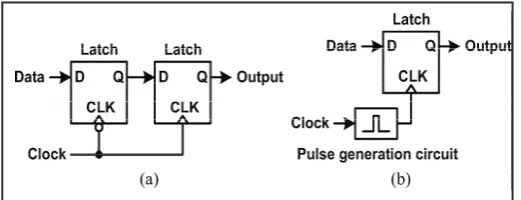
Optimized shift register designs are not achieved with the use of master-slave flip flops. Performance parameters such as area and power can be reduced with use of pulsed latches. Hence master-slave using two latches are can be replaced by pulsed latch consisting of latch with pulsed clock signal [7] which is shown in fig. 5.
Fig. 5: Pulsed Latch
III. Proposed Shift Register
Proposed work is a low-power and area-efficient shift register using pulsed latches. The shift register solves the timing problem using multiple non-overlap delayed pulsed clock signals instead of the conventional single pulsed clock signal. The shift register uses a small number of the pulsed clock signals by grouping the latches to several sub shifter registers and using additional
temporary storage latches. All pulsed latches share the pulse generation circuit for the pulsed clock signal. As a result, the area and power consumption of the pulsed latch become almost half of those of the master-slave flip-flop.
The pulsed latch cannot be used in shift registers due to the timing problem occurred in latch. The following figures show the timing problem in the shifter register. The output signal of the first latch (Q1) changes correctly because the inputs signal of the first latch (IN) is constant during the clock pulse width. But the second latch has an uncertain output signal (Q2) because its input signal (Q1) changes during the clock pulse width.
Fig. 6(a): Series Connection of Latches (Shift Register) (b) Timing Problem in Latches.
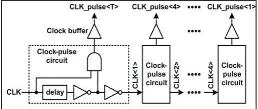
This timing problem can be overcome with the use of multiple non overlapped delayed pulsed clock signals. The delayed pulsed clock signals are generated when a pulsed clock signal goes through delay circuits. Each latch uses a pulsed clock signal which is delayed from the pulsed clock signal used in its next latch. Therefore, each latch updates the data after its next latch updates the data.
Fig. 7: Shift Register With Latches and Delayed Pulsed Clock Signals. (a) Schematic. (b) Waveforms.
to reduce the number of delayed pulsed clock signals. A 4-bit sub shifter register consists of five latches and it performs shift operations with five non-overlap delayed pulsed clock signals (CLK _pulse<1:4> and CLK _pulse<T>). In the 4-bit sub shift register #1, four latches store 4-bit data (Q1-Q4) and the last latch stores 1-bit temporary data (T1) which will be stored in the first latch (Q5) of the 4-bit sub shift register #2. Five non-overlap delayed pulsed clock signals are generated by the delayed pulsed clock generator. The operations of the other sub shift registers are the same as that of the sub shift register #1 except that the first latch receives data from the temporary storage latch in the previous sub shift register.
Fig. 8: Proposed Shift Register
When an N-bit shift register is divided into K-bit sub shift registers, the number of clock-pulse circuits is K+1 and the number of latches is N+N/K. A K-bit sub shift register consisting of K+1latches requires K+1 pulsed clock signals. The number of sub shift registers M becomes N/K, each sub shift register has a temporary storage latch. Therefore, N/K latches are added for the temporary storage latches. A 64-bit shift register with sub shift register size 4 (K=4) requires 16 sub shift registers. And each sub shift register consist of 5 latches.
Below figure is the pulse clock generator. Which gives the multiple non overlap delayed pulse clock signals for K-bit sub shift register.
Fig. 9: Non Overlap Clock Pulse Generator
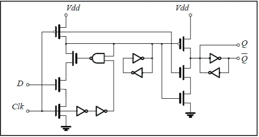
SSASPL (static differential sense amp shared pulse latch) is a smallest all pulsed latches [7]-[10]. The schematic of SSASPL is shown in below figure.
Fig. 10: Schematic of SSASPL [7]
PPCFF (power pc style flip flop) is a smallest flip flop [11]-[15] with the total number of transistors as 18. So in this paper we are compared the performance of shift register by using flip flop and pulsed latch that is PPCFF and SSASPL respectively.
IV. Schematics and Simulation Results
A. Schematics of Shift Registers
All the shift registers schematics are drawn in S-Edit of Tanner Tools and from which net lists are extracted, which are given as input files for the H-Spice. Simulations are carried out in H-Spice and wave forms are generated using Avan waves.
When counting the total number of transistors in pulsed latches and flip-flops, the transistors for generating the differential clock signals and pulsed clock signals are not included because they are shared in all latches and flip-flops. The SSASPL uses 7 transistors, which is the smallest number of transistors among the pulsed latches [7]–[9]. The PPCFF uses 16 transistors, which is the smallest number of transistors among the flip-flops [11]–[15]. Two 64-bit area-efficient shift registers using the SSASPL and PPCFF were implemented to show the effectiveness of the proposed shift register. Fig. 11 shows the schematic of the PPCFF, which is a typical master-slave flip-flop composed of two latches. The PPCFF consists of 16 transistors and has 8transistors driven by clock signals. For a fair comparison, it uses the minimum size of transistors.
Fig. 11: Schematic of PPCFF
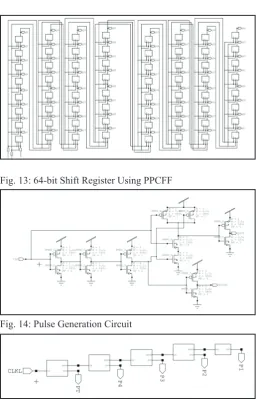
Fig. 13: 64-bit Shift Register Using PPCFF
Fig. 14: Pulse Generation Circuit
Fig. 15: Five Non-Overlapped Clock Pulses Generator
Fig. 16. Schematic of SSASPL latch
Fig. 17: 4-bit Shift Register Using SSASPL
Fig. 18: 64 Bit Shift Register Using SSASPL
B. Simulated Waveforms
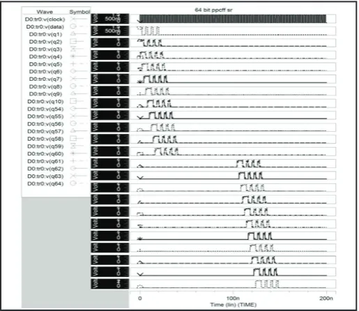
To compare the performances of the proposed shift register with the flip-flop based shift register, each circuit was designed using 180nm technology with VDD=1.8V, fCLK=100MHz, Temp=250Cand simulated with HSPICE. The Avan waves for the three comparators are shown below.
Fig. 20: Simulated Wave Forms for PPCFF 64-Bit Shift Register
Fig. 21. Simulated waveforms for SSASPL four bit shift register
Fig. 22. Simulated wave forms for SSASPL 64-bit shift register
V. PERFORMANCE COMPARISION
Table 1 shows the performance comparisons of shift registers. The conventional shift register using flip-flops was implemented with the PPCFFs. The proposed shift register using pulsed latches were implemented with the SSASPLs. The proposed shift register achieves a small area and low power consumption compared to the conventional shift register as the numbers of transistors are less.
Table 1:
Size of SR
Shift Register using
SSAPL (Pulsed Latch) Shift Register using PPCFF (Flip-Flop) Total No. of
transistors Power(mW) Total No. of transistors Power(mW) 4-BIT 103 0.227 64 0.140 8-BIT 138 0.241 128 0.224 16-BIT 208 0.274 256 0.343 32-BIT 348 0.311 512 0.373 64-BIT 628 0.313 1024 0.422
VI. Conclusion
The shift register reduces area and power consumption by replacing flip-flops with pulsed latches. A 64-bit shift register was implemented using a 0.18 um CMOS technology with vdd=1.8V at clock frequency of 100 MHz. which consumed the power and area compared to conventional method that is shift register using flip flops.
References
[1] P. Reyes, P. Reviriego, J. A. Maestro, O. Ruano,“New protection techniques against SEUs for moving average filters in a radiation environment,”IEEE Trans. Nucl. Sci., Vol. 54, No. 4, pp. 957–964, Aug.2007.
[2] V. Stojanovic, V. Oklobdzija,“Comparative analysis of masterslavelatches and flip-flops for high-performance and low-power systems”, IEEE J. Solid-State Circuits, Vol. 34, No. 4, pp. 536–548, Apr. 1999.
[3] M. Hatamianet al.,“Design considerations for gigabit ethernet 1000base-T twisted pair transceivers,” Proc. IEEE Custom Integr. CircuitsConf., pp. 335–342, 1998.
[4] H. Yamasaki, T. Shibata,“A real-time image-feature-extraction and vector-generation vlsi employing arrayed-shift-register architecture,” IEEE J. Solid-State Circuits, Vol. 42, No. 9, pp. 2046–2053, Sept. 2007.
[5] H.-S. Kim, J.-H.Yang, S.-H.Park, S.-T.Ryu, G.-H. Cho, “A 10-bitcolumn-driver IC with parasitic-insensitive iterative charge-sharing based capacitor-string interpolation for mobile active-matrix LCDs,” IEEE J. Solid-State Circuits, Vol. 49, No. 3, pp. 766–782, Mar. 2014.
[6] S.-H. W. Chiang, S. Kleinfelder,“Scaling and design of a 16-megapixelCMOS image sensor for electron microscopy,” in Proc. IEEE Nucl. Sci. Symp. Conf. Record (NSS/MIC), 2009, pp. 1249–1256.
[7] S. Heo, R. Krashinsky, K. Asanovic,“Activity-sensitive flip-flopand latch selection for reduced energy,” IEEE Trans. Very Large Scale Integr. (VLSI) Syst., Vol. 15, No. 9, pp. 1060–1064, Sep. 2007.
[9] H. Partoviet al.,“Flow-through latch and edge-triggered flip-flop hybrid elements,” IEEE Int. Solid-State Circuits Conf. (ISSCC) Dig. Tech.Papers, pp. 138–139, Feb. 1996. [10] E. Consoli, M. Alioto, G. Palumbo, J. Rabaey, “Conditional
push-pull pulsed latch with 726 flops energy delay product in 65 nm CMOS,” In IEEE Int. Solid-State Circuits Conf. (ISSCC) Dig. Tech. Papers, Feb. 2012, pp. 482–483. [11] J. Montanaroet al.,“A 160-MHz, 32-b, 0.5-W CMOS RISC
microprocessor,” IEEE J. Solid-State Circuits, vol. 31, no. 11, pp. 1703–1714,Nov. 1996.
[12] S. Nomura et al.,“A 9.7 mW AAC-decoding, 620 mW H.264 720p60fps decoding, 8-core media processor with embedded forward body-biasing and power-gating circuit in 65 nm CMOS technology,” In IEEE Int. Solid-State Circuits Conf. (ISSCC) Dig. Tech. Papers, Feb. 2008, pp. 262–264. [13] Y. Ueda et al.,“6.33 mW MPEG audio decoding on a
multimedia processor,” In IEEE Int. Solid-State Circuits Conf. (ISSCC) Dig. Tech. Papers, Feb. 2006, pp. 1636– 1637.
[14] B.-S. Kong, S.-S.Kim, Y.-H. Jun,“Conditional-capture flip-flop for statistical power reduction,” IEEE J. Solid-State Circuits, Vol. 36, pp. 1263–1271, Aug. 2001.
[15] C. K. Teh, T. Fujita, H. Hara, M. Hamada,“A 77% energy-saving22-transistor single-phase-clocking D-flip-flop with adaptive-coupling configuration in 40 nm CMOS,” In IEEE Int. Solid-State Circuits Conf.(ISSCC) Dig. Tech. Papers, Feb. 2011, pp. 338–339.
[16] 180nm Predictive Technology Model (PTM), [Online] Available: http://www.eas.asu.edu/~ptm/latest.htm [17] Philip E. Allen, Douglas R. Holberg,"CMOS Analog Circuit
Design", 2nd Ed. New York, NY: Oxford, 2002.
P. Rajesh received his B.Tech degree from Raghu Engineering College in the year 2011 and received M.Tech degree from MVGR College of Engineering in the year 2013. He is working as an Assistant Professor in the Department of Electronics and Communication Engineering at Raghu Engineering College. He has published three Papers in International Journals. His research activities are related to Low power VLSI Design.
D. Suresh Chandra presently pursuing his B.Tech in Electronics and Communication Engineering, Raghu Engineering College
L. Sai Kumar presently pursuing his B.Tech in Electronics and Communication Engineering,
Raghu Engineering College.