www.j-sens-sens-syst.net/4/25/2015/ doi:10.5194/jsss-4-25-2015
© Author(s) 2015. CC Attribution 3.0 License.
Defects and gas sensing properties of carbon
nanotube-based devices
S. Baldo1,2, V. Scuderi1, L. Tripodi1,2, A. La Magna1, S.G. Leonardi3, N. Donato3, G. Neri3, S. Filice4, and S. Scalese1
1Istituto per la Microelettronica e Microsistemi, CNR, VIII Strada 5, 95121, Catania, Italy
2Dipartimento di Fisica e Astronomia, Università degli Studi di Catania, Via S. Sofia, 95125, Catania, Italy 3Dipartimento di Ingegneria Elettronica, Chimica e Ingegneria Industriale, Università degli Studi di Messina,
Contrada di Dio, Salita Sperone 31, Messina, Italy
4Dipartimento di Chimica e Tecnologie Chimiche, Università della Calabria, Via P. Bucci, cubo 14/D, 87036,
Arcavacata di Rende (CS), Italy
Correspondence to: S. Baldo ([email protected]) and S. Scalese ([email protected])
Received: 30 July 2014 – Revised: 23 December 2014 – Accepted: 6 January 2015 – Published: 4 February 2015
Abstract. In this work we report on the development of back-gated carbon nanotube-field effect transistors (CNT-FETs), with CNT layers playing the role of the channel, and on their electrical characterisation for sensing applications. The CNTs have been deposited by electrophoresis on an interdigitated electrode region created on a SiO2/Si substrate. Different kinds of CNTs have been used (MWCNTs by arc discharge in liquid nitrogen and MWCNTs by chemical vapour deposition, CVD) and the electrical characterisation of the devices was performed in a NH3- and NO2-controlled environment. Preliminary data have shown an increase in the channel resistance under NH3 exposure, whereas a decrease is observed after exposure to NO2, and the sensitivity to each gas depends on the kind of CNTs used for the device.
Furthermore, the defect formation by Si ion implantation on CNTs was investigated by high-resolution trans-mission electron microscopy (TEM) and Raman analysis. The behaviour observed for the different devices can be explained in terms of the interaction between structural or chemical defects in CNTs and the gas molecules.
1 Introduction
Since their discovery, carbon nanotubes (CNTs) have aroused great interest due to their exceptional properties related to their one-dimensional character (Deretzis et al., 2006) like a high current-carrying capacity, high thermal conductivity and reduced charge carrier scattering. The use of both individual nanotubes and CNT networks has been explored, depending on the specific applications (Zhou et al., 2002). Currently they are used in various technological ap-plications, such as microelectronics or nanoelectronics, the automotive field, telecommunications, the aerospace indus-try, and the biomedical field.
Due to a very high surface-to-volume ratio, high electron mobility, great surface reactivity and high capability of gas adsorption, CNTs can be used as sensitive layers in gas sen-sors for environmental monitoring, industrial process
con-trol and non-invasive biomedical analysis, by exploiting the changes in their electrical characteristics induced by surface chemical modifications (Zhang et al., 2008).
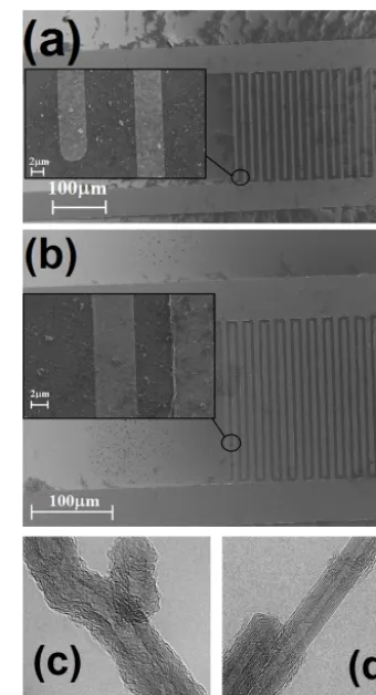
synthesised by the Sigma Aldrich CoMoCATr catalytic CVD process, hereafter called MWCNTs-CVD, and MWC-NTs synthesised by arc discharge in liquid nitrogen (LN2) and oxidised in H2O2 (diluted at 30 %) for 2 h in an ultra-sonic bath (Bagiante et al., 2010; Scalese et al., 2010), here-after called MWCNTs-LN2. The MWCNTs were deposited by the electrophoresis technique on an interdigitated elec-trode region created on a SiO2/Si n++type substrate (Baldo et al., 2014; Scuderi et al., 2012a), as reported in the scanning electron microscopy (SEM) image in Fig. 1a and b. In Fig. 1c and d, transmission electron microscopy (TEM) images are reported for both kinds of nanotubes, showing relevant dif-ferences in the structural order. The conductive Si substrate is used as a back-gate contact. The FET structure is useful in order to investigate any possible changes in the CNT elec-trical properties induced, for example, by ion implantation processes.
A complete electrical characterisation has been carried out, both in air and in controlled gaseous environments (NO2 and NH3), using two source meters (SMU) in a common source configuration, the Keithley 6487 for gate biasing and the Keithley 2400 for source and drain biasing (Fig. 2a). Both instruments, connected to a computer by the general purpose interface bus (GPIB), are totally controlled by MAT-LAB software. In this way a complete parameter analyser is obtained. The devices have been connected to the instru-ments with an appropriate test fixture (Fig. 2b) that gives the possibility of performing measurements in air and gaseous environments through an appropriate chamber connected to the gas system (Fig. 2c).
Understanding of the role of defects in the gas sensing properties of CNTs is of great relevance for the improve-ment of the sensitivity of CNT-based gas sensors. Defect for-mation by Si ion implantation on MWCNTs-LN2 was also investigated. The samples were implanted with Si+ ions at 180 keV. The used energy was fixed so that the silicon im-planted profile was fully contained in the SiO2/Si substrate. The ion doses were 1×10¹³, 5×10¹³and 1×1014cm−2.
The number of carboxyl groups has been determined by thermo-gravimetric analysis (TGA) using a Perkin Elmer Pyris 6 TGA thermo-gravimetric analyser. After reaching a thermal equilibrium at 30◦C for 5 min, the samples are heated up to 900◦C with a heating rate of 10◦min−1. The structural characterisation of the samples was performed by
Figure 1.SEM images of devices with MWCNTs-CVD (a) and MWCNTs-LN2(b). In (c) and (d), TEM images of CNTs produced, respectively, by CVD and arc discharge are reported; the latter were treated by H2O2.
SEM, using a ZEISS SUPRA 35 FE-SEM system with a field emission electron gun, and by TEM, using a JEM 2010F JEOL microscope operating with an acceleration voltage of 200 kV.
Raman scattering has been excited by a 514.5 nm radiation coming from an Ar ion laser and the scattered light has been analysed by a single 460 mm monochromator (Jobin–Yvon HR460). Laser power was always kept below 10 mW at the sample to avoid its degradation, and the accumulation time was in the range of a few minutes.
3 Results and discussion
Figure 2.(a) Measurement set-up scheme; (b) test fixture; (c) test fixture and chamber for gas exposure.
exposure to NH3 induces an increase in the channel resis-tance as the concentration of ammonia is increased, and vice versa, during the exposure to NO2, a decrease in the channel resistance is noted as the NO2concentration is increased. The response is attributed to the electrical charge transfer induced on the CNTs by the two kinds of molecules, which are elec-tron donors (NH3) or acceptors (NO2) (Donato et al., 2011). The device with MWCNTs-LN2shows a better sensitivity to NH3compared to the device with MWCNTs-CVD (Fig. 3a), while the device with MWCNTs-CVD shows a better sensi-tivity to NO2compared to the other one (Fig. 3b).
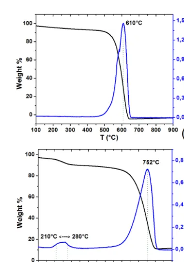
These results depend on the different interaction of the gaseous species with CNTs. In fact, the presence of the -COOH groups on the CNT walls, in the case of MWCNTs-LN2, favours an acid–base chemical interaction between the oxidised CNT and NH3molecules. NO2 molecules instead are generally adsorbed by structural defects like vacancies, which are more abundant in MWCNTs-CVD. TGA results are shown in Fig. 4, expressed as weight % or derivative
Figure 3. Sensitivity values (1R/R0) for MWCNT-CVD and MWCNT-LN2devices to NH3(a) and NO2(b).
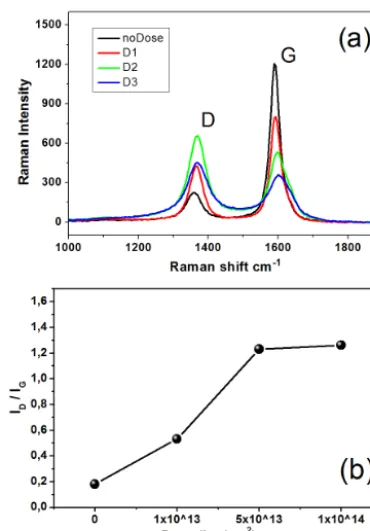
Figure 5.Raman spectra of the sample (a) not implanted (black line) and implanted with Si ion doses of 1×1013cm−2(red line), 5×1013cm−2(green line) and 1×1014cm−2(blue line); (b)ID/IG ratio vs. implant dose.
weight (left and right axes) as a function of temperature. A weight loss of 4 % between 210 and 280◦C (Fig. 4b) is ob-served in the case of MWCNTs-LN2, confirming the pres-ence of carboxyl groups (Datsyuk et al., 2008). Conversely, in MWCNTs-CVD, no weight loss is observed in that range of temperatures (Fig. 4a). In both materials, no hydroxyl functionalities, usually degrading in the temperature range 350–500◦C, are observed. Furthermore, the TGA shows that MWCNTs-LN2 are inherently less defective and therefore more stable than the other ones, since the total weight loss of carbon is obtained for higher temperatures with respect to the other kinds of nanotubes (752 vs. 610◦C).
In order to investigate the role of defects in the CNT sens-ing properties, we have introduced structural defects by ion implantation on the CNTs that show a better structural qual-ity (arc discharge synthesis). In particular, Si ion implanta-tion has been performed at 180 keV at room temperature with three doses: 1×1013cm−2(called D1), 5×1013cm−2(called D2) and 1×1014cm−2(called D3). The reference sample, not exposed to ion implantation, is called D0.
After the ion implantation, the samples were analysed by Raman spectroscopy, in order to evaluate the structural or-der of the nanotubes. The spectra were acquired at different points of each sample in order to verify the uniformity of the material deposited on the area between the electrodes. The obtained spectra showed a very similarID/IGratio for each
Figure 6.Typical CNT structures and defects observed by TEM for the samples (a) not implanted, (b) implanted with a Si ion dose of 1×1013cm−2, and (c) implanted with a Si ion dose of 1×1014cm−2.
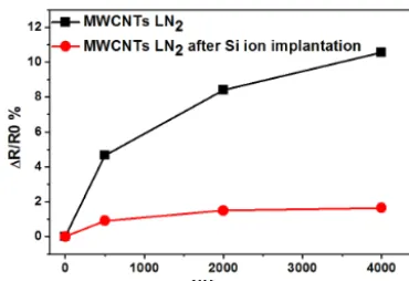
Figure 7. Comparison between 1R/R0 values obtained for MWCNTs-LN2 and MWCNTs-CVD in NH3 before (black line) and after (red line) Si implantation (Vgs=Vds=5V).
the nanotubes. Starting from the reference spectrum (black curve) related to sample D0, as the ion dose is increased, it is possible to observe an increase in the D peak intensity, a decrease in the G peak intensity and an enlargement of both. The ratio between the D and G band intensities (ID/IG) gives information on the graphitic order of C structures: in partic-ular, a lowerID/IGratio means a better structural order. The ID/IGratio calculated from Fig. 5a is reported as a function of the implant dose in Fig. 5b. As expected, the CNT struc-tural quality worsens for higher implant doses: the ID/IG value increases from 0.6 for the sample not implanted up to 1.5 for the sample implanted with a dose of 1×1014cm−2.
The samples D0, D1 and D3 were also investigated by transmission electron microscopy in order to compare the damage degrees. The TEM images, reported in Fig. 6, show the effects of ion implantation, like vacancy formation and coalescence, shell burning, and diffusion of carbon atoms inside the structure. In particular, the damage is more ev-ident for the sample implanted with the highest dose (1×
1014cm−2), shown in Fig. 6c, in agreement with the results obtained by Raman spectroscopy.
The silicon ions that arrive on carbon nanotubes with an energy of 180 keV can break the outer shell and induce mi-grations of carbon atoms on the structures. For the highest implant dose, the amorphous carbon arranges itself on the outer shell like a carbon overcoat (Fig. 6c).
The removal of carbon atoms from CNT walls leads to a rearrangement of the network from a hexagonal structure to a coherent structure also containing non-six-membered rings. In particular, the presence of pentagons and/or heptagons in the structure changes the curvature of graphene cylinders (Iijima et al., 1992; Scuderi et al., 2012b) and, furthermore, it is possible to see that external diameter shrink due to the continuous loss of atoms (Banhart et al, 2005).
In order to investigate the effect of defects induced by ion implantation (dose of 1×1013cm−2) on the sensing proper-ties, an electrical characterisation of the CNT network before and after ion implantation was done in an NH3gaseous
envi-Figure 8.Dependence ofIdsonVgsfor the CNT-FET device before and after implantation (Si ion dose: 1×1013cm−2), for a fixedVds value of 5V.
ronment. In Fig. 7, we compare the sensitivity of the device, before (black line) and after (red line) ion implantation, keep-ing the same biaskeep-ing conditions (Vgs=Vds=5V) in terms of 1R/R0. A worse response of the device is evidenced (red line) after ion implantation. Therefore, it looks like Si im-plantation has led to a deterioration in the CNT sensitivity to NH3molecules.
We guess that the removal of carbon atoms from CNT walls and the consequent rearrangement of the hexagonal lat-tice, due to ion implantation, in some way also involves the -COOH groups responsible for the NH3adsorption. In par-ticular, the removal of or the change in the -COOH groups causes a reduction in the molecules’ adsorption on the CNT walls and, therefore, a reduced sensitivity to NH3.
In Fig. 8 we report a comparison between theIds−Vgs trans-characteristics obtained for the same device before and after ion implantation (Si ion dose: 1×1013cm−2): the initial dependence ofIdsonVgsdisappears after implantation, thus indicating a transition of the electrical behaviour of CNTs from semiconducting to quasi-metallic. This behaviour is compatible with the removal of -COOH functionalities. Fur-ther experiments are still needed to understand these findings deeply.
4 Conclusions
observations, showing the presence of large holes (vacancy agglomerations) on the CNT outer walls and the presence of amorphous carbon layers on the outer surface of the CNTs.
Electrical characterisation indicates that the Si ion implan-tation has reduced the CNT sensitivity to NH3. We guess that ion implantation, in some way, removes or alters the -COOH groups responsible for the NH3adsorption.
Further studies have to be carried out in order to achieve the complete understanding of the observed behaviours and to tailor the structural properties of CNTs for the improve-ment of sensing properties of such CNT-based devices.
Acknowledgements. The authors acknowledge expert technical support by A. Marino for ion implantation processes, C. Bongiorno for TEM analysis, S. Di Franco for lithographic processes, N. God-bert for TGA analysis and the group of Prof. G. Compagnini for Raman spectroscopy.
This work has been funded by MIUR by means of the PON R&C 2007-2013 national programme, project “Hyppocrates – Sviluppo di Micro e Nano-Tecnologie e Sistemi Avanzati per la Salute dell’uomo” (PON02 00355).
Edited by: A. Romano-Rodriguez Reviewed by: two anonymous referees
References
Bagiante, S., Scalese, S., Scuderi, V., D’Urso, L., Messina, E., Com-pagnini, G., and Privitera, V.: Role of the growth parameters on the structural order of MWCNTs produced by arc discharge in liquid nitrogen, Phys. Stat. Sol. B, 247, 884–887, 2010. Baldo S., Scalese, S., Scuderi, V., Tripodi, L., La Magna, A.,
Ro-mano, L., Leonardi, S. G., and Donato, N.: Correlation between structural and sensing properties of carbon nanotube-based de-vices, Sensors – Proceedings of the Second National Conference on Sensors, Rome, Italy, 19–21 February, 2014.
otubes – From Research to Applications, 14, 229–242, 2011. Iijima, S., Ichihashi, T., and Ando, Y.: Pentagons, heptagons and
negative curvature in graphite microtubule growth, Nature, 356, 776–778, 1992.
Neophytou, N., Ahmed, S., and Klimeck, G.: Influence of vacancies on metallic nanotube transport properties, Appl. Phys. Lett. 90, 182119–182121, 2007.
Robinson, J. A., Snow, E. S., B˘adescu, ¸S. C., Reinecke, T. L., and Perkins, F. K.: Role of Defects in Single-Walled Carbon Nan-otube, Chemical Sensors. Nano Lett., 6, 1747–1751, 2006. Scalese, S., Scuderi, V., Bagiante, S., Gibilisco, S., Faraci, G., and
Privitera, V.: Order and disorder of carbon deposit produced by arc discharge in liquid nitrogen, J. Appl. Phys. 108, 064305– 064309, 2010.
Scuderi, V., La Magna, A., Pistone, A., Donato, N., Neri, G., and Scalese, S.: Use of the electric fields for the manipulation of MWCNTs, Carbon-Based Low Dimensional Materials – Pro-ceedings of the 2nd CARBOMAT Workshop ISBN 978-88-124-5, 86–89, 2012a.
Scuderi, V., Bongiorno, C., Faraci, G., and Scalese, S.: Effect of the liquid environment on the formation of carbon nanotubes and graphene layers by arcing processes, Carbon, 50, 2365–2369, 2012b.
Scuderi, V., Tripodi, L., Piluso, N., Bongiorno, C., Di Franco, S., and Scalese, S.: Current-induced defect formation in multi-walled carbon nanotubes, J. Nanopart. Res., 16, 2287–2292, 2014.
Zhang, T., Mubeen, S., Myung, N. V., and Deshusses M. A.: Recent progress in carbon nanotube-based gas sensors, Nanotech. 19, 332001–332014, 2008.