© 2017 IJSRST | Volume 3 | Issue 6 | Print ISSN: 2395-6011 | Online ISSN: 2395-602X Themed Section: Science and Technology
Phonon Controlled Temperature Dependence of Electron Mobility in 2DEG of
GaAs Surface Layer
A. K. Ghorai
Physics Department, Kalimpong College, Kalimpong, West Bengal, India
ABSTRACT
The acoustic phonon limited zero-field mobility of free electrons is estimated in a degenerate two dimensional elec-tron gas (2DEG) formed in semiconductor interface considering the effect of screening of the free carriers and the true phonon distribution which are indeed dominant characteristics of electron-phonon scattering at low lattice temperatures. Numerical calculations are made to observe the effect of screening on mobility values in GaAs surface layer and the result obtained here is compared with available experimental data and other theoretical result.
Keywords: Semiconductor, 2DEG, Mobility, Phonon, Screening.
I.
INTRODUCTION
A triangular quantum well is formed at the AlGaAs/GaAs interface and in the triangular well only the quantum mechanical ground state is populated by free electrons at low lattice temperatures ( ). Thus the system formed is regarded as one of the best experimental realizations of a two dimensional electron gas (2DEG) in nature. The transport characteristics in these systems are studied with great interest because of the very high mobility at low temperature [1-5].
Different theoretical models are adopted to study the transport properties in a 2DEG. The success of these models largely depends on a priori idea of different type of scattering mechanisms and one must know which type of scattering is predominant in a particular material under the prevalent condition of lattice temperature and free carrier concentration
At low temperatures the free carriers are dominantly scattered by the intravalley acoustic phonon and by impurity ions. The intravalley acoustic phonon scattering is the most important mechanism in controlling the electrical transport at low lattice temperatures ( ) if the impurity atoms in the system under study is relatively low [6-10]. The impurity scattering can be suppressed by dielectric engineering but the scattering by acoustic phonons is intrinsic to the semiconductor and cannot be eliminated. Thus the intrinsic mobility determined by acoustic
phonon scattering alone provides an important upper limit for the achievable mobility at low lattice temperatures. The free electrons in a covalent semiconductor interact dominantly only with acoustic phonons through deformation potential. On the other, if a semiconductor consists of dissimilar atoms such as GaAs, the bonds are partly ionic and the unit cell does not contain a center of symmetry and electrons interact with acoustic phonons due to both deformation potential as well as piezoelectric coupling [8,11,12].
Again with the lowering of lattice temperature a number of features arises which are different from those of higher lattice temperatures. To mention in particular, the effect of finite phonon energy on electron-phonon interactions, the non-equipartition energy distribution of phonons, the degeneracy of the free carrier ensemble, the electrostatic screening of the scattering potential by the electrons are dominant factors of electron-phonon scattering at low lattice temperatures. Taking all these features into account at a time it is very difficult to study the electrical transport in 2DEG and to perform the same one adopts theoretical models imparting reasonable approximations in respect of lattice temperature and carrier concentration. Some works on the study of electrical transport in 2DEG at low temperatures have already been reported by the present author [10, 13-17].
and Nakamura [19] developed a comprehensive theory of phonon limited electron mobility in a degenerate Si(100) inversion layer at low lattice temperature. Lei et al [20] have developed a non-Boltzmann theory of the steady state transport using the full phonon distribution at low temperatures and studied the transport properties in GaAs-GaxAl1-xAs heterojunctions. A theory of intravalley acoustic phonon scattering of the free carriers in a non-degenerate 2DEG has been developed by the present author [10] and the zero-field mobility of free electrons in Si inversion layers has been estimated with the help of Monte Carlo simulation of velocity autocorrelation function.
At low temperatures, the Fermi energy of the free electrons in a 2DEG is usually greater than their thermal energy and hence the electron system obeys the degenerate statistics. In degenerate 2DEG the Fermi energy is seen to be much higher than the intravalley acoustic phonon energy and hence the electron-phonon collisions are usually considered to be quasi-elastic. But unlike the traditional practice, the energy distribution of phonons cannot be approximated by the equipartition law of the Bose-Einstein distribution function in view of the low temperature range of interest here. Again with the lowering of lattice temperature the electronic system starts to be degenerate and then the effect of screening of the free carriers may significantly influence the electrical transport [3, 14, 22]. In the present article the scattering rates of the free electrons for their interaction with deformation potential as well as piezoelectric acoustic phonons are determined in a degenerate 2DEG system at low lattice temperature giving due account to the true phonon population and the effect of screening of the free electrons in the system. The scattering rates are then applied to calculate the acoustic phonon limited electron mobility as a function of lattice temperature in a degenerate 2DEG formed in GaAs inversion layer. The mobility results thus obtained in GaAs 2DEG are compared with the available experimental data and other theoretical result [23].
II.
THEORY
The electron mobility can be determined by solving Boltzmann equation in the relaxation time approximation as
〈 ( ⃗ )〉 ( )
where 〈 ( ⃗ )〉 is the average relaxation time over the
electron energies ⃗ , ⃗ is the component of the
electron wave vector parallel to the interface, is the electronic charge and is the mobility effective mass of the electron. If the electron distribution becomes degenerate the phonon-limited electron mobility in the surface inversion layer is given by [19]
( )
( )
with the Fermi energy , where
( ) is the Dirac constant, is the effective mass of the electron parallel to the interface and is the number of equivalent valleys at the surface. Now the phonon limited relaxation time of electron in III-V compound semiconductor is induced by both deformation potential and piezoelectric acoustic phonons and thus can be given by
well-known Mathiesen Rule as
( )
where is the electron mobility due to
deformation potential(DP) acoustic phonon and
is mobility due to piezoelectric coupling(PZ).
In an oxide-semiconductor interface the conduction electrons are free to propagate in the x-y plane parallel to the interface but are confined by the potential due to surface electric field in the z-direction perpendicular to the interface. For spherical constant energy surfaces the energy eigen values of the electrons in a surface channel of a triangular potential well can be expressed [5] as
⃗
* +
( )
mass perpendicular to the surface, and are the roots of the equation ( ) ( ) being Airy function.
The phonon-limited momentum relaxation time
( )( ⃗ ) of an electron induced either by
deformation potential or piezoelectric coupling with energy ⃗ in a degenerate 2DEG may be obtained
from the first order perturbation theory as[5]
( )( ⃗ )
∫
∫
( ) *|⟨ ⃗ | ( )| ⃗ ⟩| { ( ⃗ )} ( ⃗ ⃗ ⃗ )
|⟨ ⃗ | ( )| ⃗ ⟩| { ( ⃗ )}
( ⃗ ⃗ ⃗ )+ ( )
where the squared matrix element of the electron-lattice scattering due to deformation potential is given by
|⟨ ⃗ | | ⃗ ⟩|
(
) ( ) ( )
( )
The matrix element corresponding to the piezoelectric interaction of the free electrons is anisotropic because of the anisotropy of the piezoelectric tensor. However, the properly averaged squared matrix element can be given as [11,12]
|⟨ ⃗ | | ⃗ ⟩|
(
) ( ) (
) ( )
In Eq.(6) the parameter is the surface deformation potential constant given in terms of a bulk value of the deformation potential and concentration
( ) as [24]
The parameter is the surface area, is the width of the layer of lattice atoms with which the electrons can interact, is the mass density, is the component of the phonon wave vector parallel to interface and is the acoustic velocity. In Eq.(7) the parameter is the piezoelectric coupling constant of the material. is the phonon population.
( ⃗ ) is the probability of occupation of the final state ⃗ and is given by the Fermi function. The upper and lower sign corresponds respectively to the processes of absorption and emission. and are respectively, the lower and upper limits of . The screening factor ( ) can be given as [3, 21]
( )
where for degenerate 2DEG
In a degenerate 2DEG the electrons having the Fermi energy control the electron transport. The Fermi energy in degenerate 2DEG is usually much greater than the acoustic phonon energy. Thus the electron-phonon collisions may be considered to be quasi-elastic in these systems and the phonon energy
can be neglected in the energy balance equation of electron-phonon interaction. Consequently, the
distribution function ( ⃗ ) can be approximated to the Fermi distribution function ( ⃗ ) . Then integration over in Eq.(5) can be carried out yielding
( ⃗ )
[ ( ⃗ )] ( ) ( )
for deformation potential acoustic phonon scattering and for piezoelectric acoustic phonon scattering we get
( ⃗ )
[ ( ⃗ )] ( ) ( )
Here the integration
( ) ∫ ( ) ( )
[ ( ) ] ( )
At low lattice temperatures the non-equipartition of phonon distribution is approximated by the Laurent expansion as [6]
( ) ∑
̅
where , being the Boltzmann constant. are Bernoulli numbers and ̅ For the practical purpose ̅ may be taken to be 3.5.
The lower ( ) and upper ( ) limits of the integration in Eq.(10) can be deduced from the energy and momentum conservation equations for an electron
making transition from a state ⃗ to ⃗ in course of a collision accompanied by either absorption or emission of a phonon. The respective limits for both absorption and emission processes can be approximated to be and
for the electron-phonon system of interest here. Hence carrying out the integration in Eq.(10) one obtains
( ⃗ )
[ ( ⃗ )] ( ⃗ ) ( )
Here
(
√ ) ( ) ( )
, ,
√
And
( ⃗ )
⃗
[ ( ⃗ )] ( ⃗ ) ( )
Here
( )( ) √
The function ( ⃗ ) takes different forms in the
different range of electron energy. Thus when the screening effect and true phonon distribution are taken into account ( ⃗ ) takes the form
( ⃗ ) ∑
( ) [∑( ) (
)
{ ( ) (
)}
∑ ( ) ( )
{ ( ) (
)}]
̅
∑
( ) [∑( ) (
)
{ ( ) (
̅)}
∑ ( ) ( )
{ ( ) ( ̅)}]
∑( ) ( ) { (
̅) ( )}
∑( ) ( ) { ( ̅) ( )}
̅ ( )
Here
√ ⃗
( ) √ ( )
( )
( )
( ) ( ) ( )
( ) ( )
( )
√
(
√ ) ( )
√ ( )
( )
( )
( )
( )
( )
√ * √ ( ) +
√
(
√ ) ( )
( ) ( ) ( )
( )
When the screening effect is neglected one should put ( ) in Eq.(10) and then considering the true phonon distribution as given in Eq.(11) one obtains ( ⃗ ) as
( ⃗ ) ∑
( )
( ) ( )
∑
( ) ( ̅)
̅
̅ ( )
Here
( )
( )
( ) ̅ ( ̅ )
Under the condition of the equipartition law of phonon distribution, put in Eq.(11) and then if one considers the screening effect the function
( ⃗ ) takes the form as
( ⃗ ) [ ( ) (
)]
[ ( ) (
)]
[ ( ) (
)] ( )
and, under the same condition if the screening effect is neglected
( ⃗ ) ( )
III.
RESULT AND DISCUSSION
The Eqs. (12) and (13) represents respectively the scattering rates of the free electrons in a degenerate 2DEG due to deformation potential and piezoelectric interaction under different conditions prescribed by the function ( ⃗ ). It is seen that when the free carrier
screening factor and the full phonon distribution is taken into account, the dependence of scattering rates upon carrier energy and lattice temperature is very much complex. Using these scattering rates we may now calculate the mobility values of free electron in a degenerate 2DEG using Eq.(2). For an application of the above formulation, sample of GaAs is considered with the material parameter values given in Table-1.
Table-1. Material parameters of GaAs [11, 12]
Physical constants values
Deformation potential, (eV) 12.0
Effective mass ratio ( ⁄ ) 0.067
Acoustic velocity, ( ) 5.2
Density, ( ) 5.31
Piezoelectric coupling constant, 0.052
Static dielectric constant, 13.5
At low temperatures, considering the electrical quantum limit the electrons are populated in the lowest subband
[5] when the layer thickness
( ) and the number of
equivalent valleys in the present system.
For GaAs, .
In Fig.1 the effect of screening of the free electron ensemble on the electron mobility in 2DEG of GaAs surface layer controlled by the acoustic phonons at different temperatures is plotted. From the figure it is observed that the mobility values are slightly influenced by the screening effect whether the equipartition approximation of the phonon distribution is considered or not. On the other, with the lowering of lattice temperature the contribution from the true phonon distribution to the electron mobility is significant whether the screening effect is taken into account or not. At lower temperatures the mobility values obtained giving due regard to the true phonon distribution decrease sharply in comparison to those obtained under equipartition law.
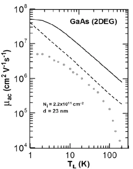
the full phonon spectrum and its equipartition approximation.
Figure 2: Lattice temperature dependence of electron mobility in GaAs 2DEG. The solid line is the result from the present theory. The dashed line and open circle ( ) symbols are respectively from the other theoretical result and the experimental data [23].
Fig.2 shows that none of the theoretical results agrees with experimental data. The reason behind the disagreement may be attributed a number of factors. At low temperatures, the electron mobility in 2DEG cannot be controlled by the surface phonon scattering only. The most dominant scattering mechanisms in 2DEG at very low temperature region are background impurity and remote impurity scattering. This apart, the information about the phonon parameters in the surface region is not properly known yet to explain the electron transport in 2DEG.
IV.
REFERENCES
[1] H. L. Stormer, Electron mobilities in modulation-doped GaAs-(AlGa)As heterostructure, Surf. Sci., 132(1-3), pp.519-526, 1983.
[2] F. Stern and W. E. Howard, Properties of semicon-ductor surface inversion layers in the electric quantum limit, Phys. Rev., 163(3), pp. 816-835, 1967.
[3] T. Ando, A. B. Fowler and F. Stern, Electronic properties of two-dimensional systems, Rev. Mod. Phys., 54(2), pp. 437-672, 1982.
[4] T. Sah, T. N. Ning and L. T. Tschopp, The scattering of electrons by surface oxide charges and by lattice vibrations at the silicon-silicon dioxide interface, Surf. Sci., 32(3), pp. 561- 575, 1972.
[5] Y. Wu and G. Thomas, Two-dimensional electron-lattice scattering in thermally oxidized silicon surface-inversion layers, Phys. Rev. B, 9(4), pp. 1724-1732, 1974.
[6] C. Jacoboni and L. Reggiani, The Monte Carlo method for the solution of charge transport in semiconductors with applications to covalent materials, Rev. Mod. Phys., 55(3), pp. 645-705, 1983.
[7] A. K. Ghorai and D. P. Bhattacharya, Effect of non-parabolic band on the scattering rates of free electrons in high purity semiconductors at low lattice temperatures, phys. stat. sol.(b), 163, pp. 247-258, 1991.
[8] A. K. Ghorai and D. P. Bhattacharya, Effect of finite-energy acoustic phonons on the zero-field mobility characteristics of high-purity semiconductors at low lattice temperatures, Phys. Rev. B, 47(20), pp.13858-13860, 1993.
[9] A. K. Ghorai and D. P. Bhattacharya, Electron transport in GaAs at low lattice temperatures, phys. stat. sol.(b), 197, pp. 125-136, 1996.
[10] A. K. Ghorai and D. P. Bhattacharya, Lattice-controlled electron transport characteristics in quantized surface layers at low temperature, Surf. Sci., 380(2-3), pp. 293-301, 1997.
[11] L. Reggiani, Hot-Electron Transport in
Semicon-ductors, Springer-Verlag, Berlin, 1985.
[12] B. R. Nag, Electron Transport in Compound
[13] A. K. Ghorai and D. P. Bhattacharya, Lattice-controlled mobility in quantized surface layers at low temperature, J. Appl. Phys., 80(5), pp.3130-3132, 1996.
[14] A. K. Ghorai, Effect of Screening on Acoustic Phonon
Limited Electron Mobility in Quantized Surface Layer in Semiconductor, IJSETR, 2(7), pp.1453-1457, 2013.
[15] A. K. Ghorai, Acoustic Phonon Limited Cross Section
for the Capture of an Electron by an Attractive Trap in Semiconductor Inversion Layer, IJSR, 4(2), pp. 1837-1840, 2015.
[16] A. K. Ghorai, Field-Dependent Electron Temperature
due to Electron–Phonon Interaction in a 2DEG at Low Lattice Temperature, J. Atoms and Molecules, 7(3), pp. 1056-1062, 2017.
[17] A. K. Ghorai, Lattice controlled hot electron mobility
in 2DEG at low temperature, IJSER, 5(7), pp.195-198, 2017.
[18] H. L. Stormer, L. N. Pfeiffer, K. W. Baldwin and K. W.
West, Observation of a Bloch-Grüneisen regime in two-dimensional electron transport, Phys. Rev. B, 41(2), pp.1278-1281, 1990.
[19] Y. Shinba and K. Nakamura, Phonon-limited electron
mobility in Si(100) inversion layer at low temperatures, J. Phys. Soc. Japan, 50(1), pp.114-120, 1981.
[20] X. L. Lei, J. L. Birman and C. S. Ting, Two
dimensional balance equations in nonlinear electronic transport and application to GaAs-GaAlAs hetero-junctions, J. Appl. Phys. 58(6), pp.2270-2279, 1985.
[21] J. Shah, Hot carriers in semiconductor nanostructures:
physics and applications, Academic Press Inc, New York, 1992.
[22] P. J. Price, Two-dimensional electron transport in
semi-conductor layers II: Screening, J. Vac. Sci. Technol., 19(3), pp.599-603, 1981.
[23] W. Walukiewicz, H. E. Ruda, J. Lagowski, and H. C. Gatos, Electron mobility in modulation doped hetero-structures, Phys. Rev. B, 30(8), pp. 4571, 1984.
[24] E. Vass, R. Lassnig, and E. Gormic, Proc of workshop
on IVth international conference of electronic
properties of 2D systems, New London, USA, 24-28
![Table-1. Material parameters of GaAs [11, 12]](https://thumb-us.123doks.com/thumbv2/123dok_us/9108216.1445164/5.595.306.545.453.685/table-material-parameters-gaas.webp)