Reconfigurable Reduced Delay Universal
Adder
MOHIT TYAGI
Electronics and Communication Department
Priyadarshini College of Computer Sciences, Greater Noida, India-201308
SAMENDER SINGH Computer Science Department
Priyadarshini College of Computer Sciences, Greater Noida, India-201308
KAVITA KHARE Electronics Department
Maulana Azad National Institute of Technology (MANIT)-Bhopal, India-462051
Abstract—This paper introduces a novel architecture for least latency universal adder using pipeline and parallel computing technique. The proposed architecture implemented in reconfigurable technology as a run time reconfigurable unit. The proposed 32-bit Universal adder design and compared with previously proposed adder designs in terms of area and delay after synthesis targeting on 4vfx60ff672-12 Xilinx virtex-4 FPGA and have high hardware resource sharing up to 42% for the binary and BCD arithmetic operations. Synthesis results show that the proposed design has the smallest delay (8.2ns) and throughput of 121.9 MOPS (at least 20% faster) with almost equivalent area-delay product when compared to other existing proposal.
Keywords –Universal adder, pipeline, parallel, hardware sharing.
1 Introduction
As we dealing with the era of electronics computing based commercial, financial, internet and industrial control applications, such type of applications needs preciseness of expression for different data representation notations and in format conversion between them. Mostly computing application based on Binary arithmetic, but the real problem is that binary approximation not creates correct results, if we use it in place of exact decimal fraction even subsequent arithmetic is correct. Therefore, in order to overcome and encounter from Binary approximation, we need a solution to avoid such incorrect approximation, binary Decimal Arithmetic is a possible solution for this position. Also, in most application Decimal software running on custom binary hardware in order to produce precise Decimal results, but the another problem is that excessive delays are encounter due to software implementation of Decimal Arithmetic is about 100 to 1000 times slower than the Binary implementation in hardware. Therefore, readily adaptable hardware solutions for both decimal and binary Arithmetic are considered in this paper. The architecture has been designed to have high hardware resources utilization and minimum delay achieved by pipelined & parallel computation, and capable of performing unsigned/signed magnitude operation by used the effective addition/subtraction approach for binary and BCD notations.
The remainder of this paper is organized as follows. Section 2 provides a brief mathematical background of BCD and the related work done regarding Binary and BCD addition on FPGAs. Section 3 gives the details of reconfigurable reduced delay universal Adder design. The experimental results analysis and comparisons to the existing design are given in section 4. Finally, a conclusion is presented in section 5.
2. Background for BCD arithmetic
11112) for decimal digit from 10 to 15 are left unused when decimal computing is considered. Assuming two decimal numbers are added using a 4-bit binary adder. The following steps are performing for BCD addition:
1. Add two 4-bit BCD numbers (equivalent to decimal digit) using binary addition.
2. If 4-bit sum is equal to or less then 9, the sum is valid BCD number and no correction is needed. 3. If the 4-bit sum is greater than or if a carry is generated from the sum is invalid BCD number. Then, the
digit 6 (01102) should be added to the sum to correct the invalid BCD representation.
In case of decimal subtraction, additional processing needed for 10’s complement of the subtrahend. As the BCD code do not include a code for decimal digit 10 and for this reason a nine’s complement representation is used and generate carry from the sum is again added to the sum.
2.1 Related work
In this section, an overview is given for five binary and decimal adder / subtractor that have already been designed. Some of the initial contribution were designed by Schmooklar et al.[1] and Adiletta et al. [2]. Later, combined of Binary and BCD adders were designed by Levine et al.[3] and Anderson[4], while first BCD sign-magnitude adder/subtractor was designed by Grupe [5]. An area efficient sign-sign-magnitude adder was later developed by Hwang [6] as shown in fig.1. Area occupied by this design was least amongst all the previous designs.
Figure 1. Hwang’s proposal [6]
Flora [7] followed the principle of carry select adders and came up with a design which concurrently process two results, one assuming the presence of an input carry and the other assuming in its absence. Fischer et al. [8] (Fig. 2) later came up with a compact design that employed only one adder but the latency was a problem as it had to use an additional correction block.
Figure 2. Fischer’s Proposal [8]
During the last decade various BCD adder/subtractordesigns have been developed for the IBM S/390, G4, G5, G6 and eServer Z900 microprocessorsbased on the design presented by Haller et al. [9].
obtain correct difference, hence increasing the latency. Recently, Haller et al.optimized the carry chain in the same architecture whichslightly reduced the delay but with an increased area of theunit.
Figure 3. Haller’s proposal (Z900)
The design of the Universal Adder (Fig. 4) proposed by D.R.Humberto et al. [10] uses effective addition/subtraction operations on unsigned/sign-magnitude, and various complement representations. This design has high latency, but overcomes thelimitations of previously reported approaches that producesome of the results in complement representation whenoperating on sign-magnitude numbers. This design proposed that the majordisadvantage of the previous designs i.e. having thesubtrahend the smaller number in magnitude, was eliminated by their approach.
Figure 4. Humberto’s Proposal [10]
Figure 5. Sreehari’s Proposal [11]
The pre-computation block consists of logic to compute propagate and generate signals for both BCD and Binary addition/subtraction. This employs a new method of subtraction unlike theexisting designs which mostly use 10’s complements, toobtain a much lower latency.
4. Reconfigurable Reduced Delay Universal Adder
The main objective of our design was to reduced delay of binary and BCD adder/subtrator operations using parallelizing and pipelining scheme. To achieve this we used the Humberto [10] design as a base. We kept its functionality as it is, with minimizing its delay. For unsigned and sign-magnitude addition/subtraction or effective addition/subtraction, we also use s/370 sign-magnitude adder [12] as a base.
Let us assume N1 and N2 being two n-bit sign-magnitude numbers, such that N1 = [N1n−1 N1n−2...N10] and N2 =
[N2n−1N2n−2...N20], with N1n−1 and N2n−1 used as sign bits of binary or BCD representations. The two modified sign bits are computed as follows:
N1S = N1n−1 · Sign (1.1)
N2S = N2n−1 · Sign (1.2)
Where input Sign = 0 signal, in the case of unsigned and complement representations. Otherwise signed representation will be performed.
Consider the operation SUM= N1 Add N2, with input signal Add indicates desirable addition/subtraction and
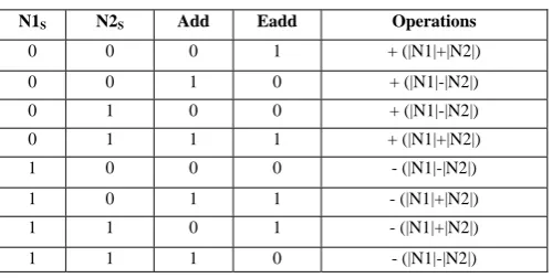
SUM being the result of the operation. The addition/subtraction operation of two unsigned-magnitude numbers decided by Add input signal (Add=0 for addition & Add=1 for subtraction), while for signed-magnitude numbers addition/subtraction operation performed by the sign bits and Add input signal. Conclusion is that the addition/subtraction of two unsigned/signed- magnitude numbers can be performed with the determination of effective operation.
Assuming the operation involves true value of the signed numbers. The effective operation can be computed by the following Boolean expression:
Eadd = (N1S ) (1.3)
Table 1. Effective operations
N1S N2S Add Eadd Operations
0 0 0 1 + (|N1|+|N2|)
0 0 1 0 + (|N1|-|N2|) 0 1 0 0 + (|N1|-|N2|) 0 1 1 1 + (|N1|+|N2|) 1 0 0 0 - (|N1|-|N2|)
1 0 1 1 - (|N1|+|N2|) 1 1 0 1 - (|N1|+|N2|)
1 1 1 0 - (|N1|-|N2|)
The computation of the magnitude of the SUM can be achieved by the following. Assume that the effective addition/subtraction operation is performed on the absolute values of N1 and N2, denoted by |N1| and |N2|
respectively, and assume that the operation produces no overflow.
Assume that the operation is binary effective addition. Then the following equation establishes binary effective addition:
SUM= |N1|+|N2|+ Co (1.4)
Where, Co is used to find whether |N1| is greater than |N2| or less than/equals to |N2|.Co should be equals to zero for effective addition. Boolean expression for Co can be defined as following:
Co= G0n-1 [|N1|, |N2|]
=Gn-1| (Pn-1.Gn-2)|...| (Pn-1.Pn-2…Pn-i.Gi)|…..
| (Pn-1.Pn-2……P1.G0) (1.5)
Where Gi = N1i.N2i and Pi=N1i|N2i are generate and propagate signals respectively.
Assume that the operation is binary effective subtraction and all possibilities can be defined as following:
Case 1: If |N1|>|N2| then SUM will be positive and the following equation establishes binary effective subtraction:
SUM= |N1|+|N2|+ Co (1.6)
Where Co =1 because |N1|>|N2| and performs 2’s complement subtraction.
Case 2: if |N1|<|N2| then SUM will be negative and the following equations establish binary effective subtraction:
SUM= |N1|+|N2|+ Co (1.7)
Where Co=0 because |N1|<|N2| and SUM itself in one’s complement representation to represent negative SUM.
Case 3: if |N1|=|N2| then sum will be zero and the following equations establish binary effective subtraction:
SUM= |N1|+|N2|+ Co (1.8)
Where Co=0 because |N1|=|N2|.
In order to generate a correct sign-magnitude result, an additional correction step is used. The final magnitude result becomes:
The SC is computed as follows:
SC= Co.Eadd (1.10)
Finally, the sign bit of the result is updated as shown equation 1.11 [12].
SUMn-1= [N1n-1 ] (1.12)
With SUM represents SUM equal to zero.
3.1 Decimal arithmetic addition
In this section we describe in more details of additional additions to the original binary adder needed for decimal addition/subtraction operations.
Assume that the operation is decimal effective addition. Then the following equation establishes decimal effective addition:
SUM= |N1|+|N2|+01102 + 0 (if DC=1) (1.13)
SUM= |N1|+|N2| + 0 + 0 (if DC=0) (1.14)
Assume that the operation is decimal effective subtraction and all possibilities can be defined as following: Case 1: If |N1|>|N2| then SUM will be positive and the following equation establishes decimal effective subtraction:
SUM= |N1|+|N2*|+ 01102+1 (if DC=1) (1.15)
SUM= |N1|+|N2*| + 0 + 0 (if DC=0) (1.16)
Where ‘*’ indicates nine’s complement of the operand.
Case 2: if |N1|<|N2| then SUM may be negative and the following equations establish decimal effective subtraction:
SUM= |N1|+|N2*|+ 11002 + 0 (if DC=1) (1.17)
SUM= |N1|+|N2*|+01102 + 0 (if DC=0) (1.18)
Case 3: if |N1|=|N2| then sum and DC signal will be zero and the following equations establish decimal effective subtraction:
SUM= |N1|+|N2*|+01102 + 0 (1.19)
The digital carry logic (DC) [13] signal for decimal operations are obtained as follows:
DC=A|B.Cin (1.20)
Where
A=G3|P3.P2|P3.P1|G2.P1
B=P3|G3|P2.G1
The final digital carry logic can be determined by the Boolean equation (1.21) which is a modified version of equation (1.20).
DC=A|B.Cin (1.21)
A=G3|P3.P2|P3.P1|G2.P1|P3.G0|G2.G0
B=P3|G3|P2.G1
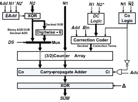
In the proposed adder illustrated in Figure 6, Eadd logic controls one’s complement operation of the subtrahend in binary and decimal operations. The nine’s complement computation for the subtrahend is performed using one’s complement then “DigitWise-6” (DW) hardwired logic, as used in many previous designs [9]. The DW value ND = N2−610 is obtained with the following equations that modify each bit of the BCD nibble as follows:
ND[3] = N2[3] · N2[2]|N2[3] · N2[1]|N2[3] · N2[2] · N2[1]
ND[2] = N2[2] N2[1]
ND[1] = N2[1]
ND[0] = N2[0]
Please note that when a binary operation is performed Bin = 1 the decimal correction term is not needed and left inactive, otherwise decimal operations are performed. The reduced delay binary and BCD adder is set up with the aforementioned logic, two carry-propagate-adder, some multiplexers and de-multiplexers, and a set of XOR gates. The final organization is depicted in Figure 6. Note that the input N2* for computing the digit carry logic is equal to nine’s complement when processing decimal subtraction. When processing decimal addition N2* is equal to N2 otherwise left inactive. The multiplexer signal control for decimal subtraction or any addition (DSS) is computed by:
DSS = Eadd · Bin (1.22)
The final complement operation is controlled by equation (1.10):
SC= (Co · Eadd)
Figure 6.Architecture for reduced delay universal adder
The whole architecture of the reduced delay universal adder sub- divided into six subunits. Sixth subunit is Carry in circuitry for both carry-propagate-adder including Co logic works parallel to the rest design. The first subunit of our proposal includes Eadd logic, XOR and Digitwise-6 logic while second subunit includes DC logic and decimal correction coder. Third and fourth subunits are carry-propagate-adder 1 and carry-propagate-adder 2 respectively. The SUM correction SC logic divides as a fifth subunit.
second and fourth subunits are left unused. And in order to perform decimal operation, first five subunit works together in pipelined manner while sixth subunit in parallel. Second subunit follows first subunit and fourth subunit follows third subunit.
When our proposed design mapped on partially reconfigurable hardware platform, the dark modules (shown in figure 6: the Carry-propagate-adder 1, the Eadd logic, the two XOR logic blocks for one’s complement of input subtrahend and output SUM and the carry in logic circuitry including Co logic) are reused in both binary and BCD operation modes.
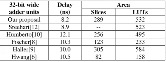
4. Experimental results analysis and comparisons
The proposed binary and BCD adder was implemented using Verilog HDL, synthesized, functionally tested, and evaluated using the ISE 9.2i Xilinx design tools targeting 4vfx60ff672-12 VIRTEX 4 FPGA device. Furthermore, the designs proposed by Fischer [8], Hwang [6], Haller [9], Humberto[10] and sreehari[12] were also implemented and synthesized using same methodology. Table 2, summarizes the latency and hardware utilization result for all of the considered designs.
Table 2.Adder Comparison in terms of Area & Delay
32-bit wide adder units
Delay (ns)
Area
Slices LUTs
Our proposal 8.2 289 532
Sreehari[12] 8.9 -- 523
Humberto[10] 12.1 256 495
Fischer[8] 10.3 123 233
Haller[9] 10.0 305 584
Hwang[6] 10.5 82 158
In terms of latency the Sreehari proposal is best so far. Compared to it, our proposal is 10% faster with using almost equal hardware resources (LUTs) and in terms of area Hwang’s proposal is best design so far, but has the deficiency to produce
“- -” not specified by author
Correct result in cases when N1< N2 for BCD subtraction operations as described by humberto[10] .
5. Conclusion
This paper presents a modified architecture for fast effective binary and BCD addition/subtraction with some additional hardware. The design is runtime reconfigurable or can be implemented in ASIC as a runtime configurable unit and low latency and maximum utilization of hardware resource are the feature of the proposed architecture. All the subunits have been designed to work with least delay. The modified unit and base unit were synthesized for 4vfx60ff672-12 Xilinx virtex 4 FPGA for comparison. Our design has 8.2ns delay and achieve throughput of 121.9 MOPS with similar area-delay product when compared to the other proposals.
References
[1] M.S.Schmookler and A. Weinderger. “Decimal Adder for Directly Implementing BCD Addition Utilizing Logic Circuitry”, InternationalBusiness Machines Corporation,US patent 3629565, pages 1 – 19, Dec 1971.
[2] M. J. Adiletta and V. C. Lamere. “BCD Adder Circuit”. DigitalEquipment Corporation, US patent 4805131, pages 1 – 18, Jul 1989. [3] S. R. Levine, S. Singh, and A. Weinberger. Integrated Binary-BCD Look-Ahead Adder. International Business Machines
Corporation, US patent 4118786, pages 1–13, Oct 1978.
[4] J. L. Anderson. Binary or BCD Adder with Precorrected Result. Motorola, Inc., US patent 4172288, pages 1–8, Oct 1979. [5] U. Grupe.“Decimal Adder“, Vereinigte Flugtechnische Werke-Fokker gmbH, US patent 3935438, pages 1 – 11, Jan 1976.
[6] S. Hwang. “High-Speed Binary and Decimal Arithmetic Logic Unit”, American Telephone and Telegraph Company, AT&T Bell Laboratories,US patent 4866656, pages 1-11, Sep 1989.
[7] Flora, Laurence P., “Fast BCD/Binary Adder”, US Patent 5007010.
[8] H. Fischer andW. Rohsaint. “Circuit Arrangement for Adding or Subtracting Operands Coded in BCD-Code or Binary-Code”, SiemensAktiengesellschaft, US patent 5146423, pages 1 – 9, Sep 1992.
[9] W. Haller, W. H. Li, M. R. Kelly, and H. Wetter. “Highly Parallel Structure for Fast Cycle Binary and Decimal Adder Unit”. InternationalBusiness Machines Corporation, US patent 2006/0031289, pages 1 – 8, Feb 2006.
[11] Sreehari Veeramachaneni, M, Kirthi Krishna; V, Prateek G, S. Subroto, S, Bharat, M.B.Srinivas, “A Novel Carry-Look Ahead Approach to a Unified BCD and Binary Adder/Subtractor”, 21st International Conference on VLSI Design 2008, pages 547-552, Jan 2008.
[12] S. Vassiliadis, D. Lemon, and M. Putrino. s/370 Sign-Magnitude Floating-Point Adder. IEEE Journal of Solid-State Circuits, pages 1062 – 1070, Aug 1989.
![Figure 1. Hwang’s proposal [6]](https://thumb-us.123doks.com/thumbv2/123dok_us/9653434.1493150/2.595.180.423.540.670/figure-hwang-s-proposal.webp)
![Figure 5. Sreehari’s Proposal [11]](https://thumb-us.123doks.com/thumbv2/123dok_us/9653434.1493150/4.595.178.402.71.243/figure-sreehari-s-proposal.webp)