NUMERICAL INVESTIGATION OF
JUNCTION TEMPERATURE EFFECT
ON DC PARAMETERS OF SILICON
IMPATT DEVICE
ARPAN DEYASI
Department of Electronics & Communication Engineering RCC Institute of information Technology, Canal South road, Beliaghata
Kolkata, West Bengal-700015, INDIA [email protected]
SWAPAN BHATTACHARYYA Department of Computer Science & Engineering Asansol Engineering College, Vivekananda Sarani, Asansol
Burdwan, West Bengal-713305 [email protected]
Abstract:
An extensive simulation is carried out to estimate the effect of junction temperature on electric field, avalanche width, breakdown voltage and efficiency based on a double iterative computer method developed on simultaneous numerical solution of Poisson’s equation, carrier diffusion equation, continuity equation in addition with the effect of mobile space charge subject to appropriate boundary conditions for electric field and normalized current density at depletion layer edges for Si DDR IMPATT structure designed at 94 GHz. Current density and junction temperature are varied for simulation purpose to obtain optimized device performance in continuous wave (CW) mode during steady state. It may be noted that with the increasing bias current density, space charge effect degrades performance of the device as far as breakdown voltage, avalanche width and efficiency are concerned. The simulation results presented will be useful to realize experimentally Si IMPATT’s for millimeter and sub-millimeter wave bands.
.
Keywords: Double-Iterative Method, Junction temperature, Space-Charge effect.
1. Introduction
Microwave and millimeter-wave transit-time devices offer a lot of advantages due to its smaller size, higher accuracy, lighter weight and lower cost, and an improved propagation characteristic at window frequencies. Thus solid-state CW and pulsed sources are designed as microwave sources associated with RADAR systems and guided missiles, as gigahertz and terahertz domain is now enriched with the immense application possibilities in the fields of Remote Sensing, Imaging and Spectroscopy. In last two decades, development of suitable reliable high-power sources in lower terahertz domain is extensively researched and new materials in various forms are explored for achieving those objectives.
efficiency, but with increase of bias current density, the problem of higher junction temperature come to the focus [15]-[16] where mobile space-charge effect and parasitic series resistance degradation are analyzed by generalized numerical algorithm. The workers studied the effect for InP material [15] which was previously carried out by & Mains etc. [17] with a different numerical method and Ray et. al. [18]. But extensive work is not yet performed on this physically establish problem, though design of heat sink are reported recently in some literatures [19]-[20].
The present paper deals with the effect of junction temperature on dc properties of symmetric DDR Si-IMPATT diode for optimized bias current density, which was numerically evaluated by double iterative computer technique involving simultaneous solution of Poisson’s equation with continuity equation [21] satisfying appropriate boundary conditions. Mobile space charge effect is also incorporated with the consideration of 1-D model where saturated carrier velocities [22] are assumed to be independent of electric field throughout the space-charge layer. Distortion of electric field at higher current density is established with simultaneous study about degradation of avalanche width and dc-to-rf conversion efficiency for different junction temperatures. Breakdown voltage also increases with current density and peak electric field enhances with junction temperature at optimized current density. Simulation results cover a wide range of temperature for better understanding of the physical effects.
2. Properties of DDR IMPATT
The frequency of operation of IMPATT diode essentially depends on transit time of charge carriers, which, in turn, is a function of depletion layer width and saturated drift velocities of carriers. For Ka-band simulation, operating frequency is considered
f
v
W
dep=
0
.
37
s (1)The prime action underlying IMPATT behavior is avalanche breakdown due to high electric field. Transit time of charged carriers is related to avalanche process as
[
]
dx
A
W
n
p
=
−
0
exp
α
β
τ
τ
(2)where α and β are ionization coefficients related with electric field and temperature by some empirical relations, and expressions are varied in different electric field ranges. For DDR IMPAATT, due to the presence of both types of carriers, transit time is given by
(
)
(
)
1 0exp
1
−
−
−
+
−
=
dx
A W n
eff
τ
κ
κ
α
β
τ
(3)where κ is the injection ratio, and WA is avalanche width. According to Scharfetter & Gummel, conversion efficiency can be computed using the approximated formula
dep A
V
V
+
=
1
1
1
π
η
(4)where breakdown voltage VB is the sum of voltage drop across avalanche region and voltage drop across drift region. It is calculated by integrating the spatial electric field over the total depletion layer width
=
2 1)
(
x xB
E
x
dx
V
(5)where boundaries are defined corresponding to the depletion layer widths of the sides.
3. Simulation Method
E
(
x
)
q
[
N
N
p
(
x
)
n
(
x
)]
x
=
D−
A+
−
∂
∂
ε
(6) Continuity equations for electron and hole current are given byn p
g
U
npx
J
q
p
n
t
,,
1
)
,
(
+
−
∂
∂
=
∂
∂
(7)In this analysis, we excluded the contribution of Un,p because the transit time of carriers in the depletion layer of the device is several orders of magnitude lower than the recombination time.
If the diffusion component of current caused by carrier concentration gradient in the space charge layer is considered, then expressions of Jn and Jp are given by-
,
(
,
)
, ,(
n
,
p
)
x
qD
v
p
n
q
J
n p n p n p∂
∂
+
=
(8)Considering contributions of both diffusion current and drift current, former has been considered as a perturbation term over the major drift current in the avalanche region. Using perturbation technique, the expressions for hole and electron concentration in the space charge layer (considering both diffusion and drift) can be written as-
.. ,
) )( ,
( 3,
3 4 , 3 , 2 , 2 3 , 2 , , 2 , , , + ∂ ∂ − ∂ ∂ + ∂ ∂ − = x J qv D x J qv D x J qv D qv J x p
n np
p n p n p n p n p n p n p n p n p n p n (9)
Hence the mobile space charge density due to both drift and diffusion components is obtained fro the equation-
.. ... )
( 2 2 +
∂ ∂ + ∂ ∂ + − = x J v D x J v D v J v J x n n n p p p n n p p
ρ
(10)Boundary conditions for the electric field in the depletion region can be written as
E
(
−
x
1)
=
E
(
x
2)
=
0
(11)where -x1 and x2 define the edges of p and n layers respectively. The boundary conditions for normalized current densities are given by
(
−
1)
=
2
−
1
pM
x
k
(12.1)and
n
M
x
k
(
2)
=
1
−
2
(12.2)where ps ns p n
J
J
M
. 0,
=
are computed consideringJ
p−
J
n=
0
.
95
J
0, extension of avalanche zone hasbeen defined as the distance between two points (x1, x2) on either side of avalanche center.
4. Numerical Results
Fig 1. Impact ionization coefficient for electron with electric field for different lattice temperature
Fig 2. Impact ionization coefficient for hole with electric field for different lattice temperature
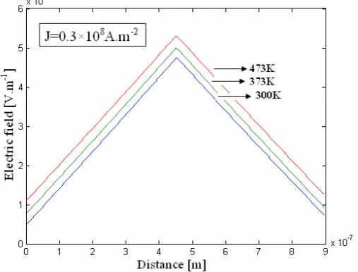
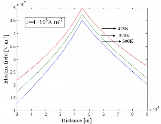
Spatial field distribution is one of the most important features for DDR structure which ultimately gives the position of metallurgical junction. With increasing junction temperature, electric field increases for specified current density, and profile indicates the fact that for lower current density, field distribution remains unperturbed. This is evident from fig 3, but fig 4 suggests that for higher current density, field distorted, and perturbation increases with increasing temperature. Comparative study also reveals the fact that for lower active area of the device, at a constant junction temperature, field becomes distorted.
Fig 4. Spatial electric field variation at different junction temperature at higher current density
Another interesting physical phenomenon can be noted from this study is with increase of current density at a specified temperature, peak electric field becomes less, but it can be increased by increasing junction temperature. Thus an optimization is required for better device performance, as evident from fig 5 & fig 6.
Fig 5. Variation of maximum electric field with current density for different junction temperature
Avalanche region extends itself with increasing current density. At higher junction temperature, avalanche region is wider than it’s counterpart at lower temperature for same current density. So it increases with both current density and junction temperature.
Fig 7. Profile of avalanche width with current density at different junction temperature
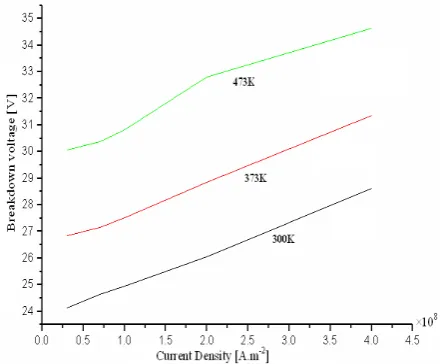
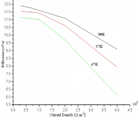
Increase of electric field will cause the increase of breakdown voltage, and since field increases with increasing temperature at a particular current density, so breakdown voltage increase due to the same physical effect. Also at a particular junction temperature, breakdown voltage slowly increases almost in a resistive fashion. Due to this combined factor, conversion efficiency drastically decreases with increasing current density, and ultimately becomes equal to the efficiency of SDR device designed with same doping concentration. Also increasing junction temperature has a profound effect on efficiency and it reduces with higher temperature, as evident from fig 9.
Fig 9. Profile of conversion efficiency with current density at different junction temperature
From the graph, it may be concluded that upto a specified current density for a particular junction temperature, conversion efficiency remains almost constant, and linearity of the profile may be extended more with reduction of junction temperature, which is very much essential from application point-of-view.
5. Conclusion
This analysis provides an insight about variation of several d.c parameters variation of different dc and ac parameters with junction temperature and current density required for small-signal analysis of the DDR device to extract the arc parameters, which will help to study the microwave performance of the device. Optimization of current density becomes essential to nullify the degradation of conversion efficiency, which is also a function of the junction temperature. Effect of mobile space charge is considered to make the analysis more realistic. Higher current density also causes a degradation of spatial electric field profile which affects performance of the device. It may be concluded that proper heat sink material is required to compensate the effect of elevated junction temperature so that device may be operated closer to terahertz region.
References
[1] Mukherjee,M; Banerjee,S; Banerjee,J.P. (2010). Dynamic Characteristics of III-V and IV-IV Semiconductor Based Transit Time Devices in the Terahertz Regime: A Comparative Analysis, Terahertz Science and Technology, 3, pp 97-109.
[2] Siedel,T.E; Davies,R.E; Iglesias,D.E. (1971). “Double-Drift-Region Ion-Implanted Millimeter-Wave IMPATT Diodes, Proceedings of the IEEE, 59, pp 1222-1228.
[3] Mukherjee,M; Banerjee,J.P. (2010). DDR Pulsed IMPATT Sources at MM-Wave Window Frequency: High-Power Operation Mode, International Journal of Advanced Science and Technology, 19, pp 1-11.
[4] Banerjee,S; Mukherjee,M; Banerjee,J.P. (2010). Bias current optimization of Wurtzite-GaN DDR IMPATT diode for high power operation at THz frequencies, International Journal of Advanced Science and Technology, 16, pp 11-20.
[5] Mukherjee,M; Banerjee,S; Banerjee,J.P. (2009). Mobile space-charge effect on Terahertz properties of Wz-GaN based DDR IMPATT oscillators, 4th CODEC.
[6] Mukherjee,M; Banerjee,S; Banerjee,J.P. (2009). MM-wave performance of DDR IMPATT’s based on cubic SiC, XVth IWPSD.
[7] Banerjee,S; Mukherjee,M; Banerjee,J.P. (2010). Studies on the performance of Wz-GaN DDR IMPATT diode at optimum bias current for THz frequencies, 3rd IEEE MiNDSS.
[8] Mukherjee,M. (2008). Prospects of α-SiC and β-SiC based p+pnn+ IMPATT devices as sub-millimeter wave high power sources,
Proceedings of International Conference on Microwave.
[9] Mukherjee,M; Roy,S.K. (2009). Wide band gap III-V Nitride based avalanche transit time diode in Terahertz regime: Studies on the effect of punch-through on high frequency characteristics and parasitic series resistance of the devices, Current Applied Physics, 10, pp 646-651.
[10] Mukherjee,M; Mazumder,N. (2008). Modeling of high power 0.3 THz IMPATT oscillator based on SiC and growth of 3C-SiC on Si <100> substrate for possible IMPATT fabrication, ICMMT.
[11] Bi,X; East,J.R; Ravaioli,U; Haddad,G.I. (2005). Analysis and Design of Si Terahertz Transit-Time Diodes, 16th International Symposium on Space Terahertz Technology, pp 271-275.
[12] Zemliak,A; Cabrera,S. (2006). Comparative Analysis of High Frequency Characteristics for DDR and DAR IMPATT Diodes, Journal of Computational Electronics, 5, pp 401-404.
[13] Xizeng,F; Wenmiao,S. (1987). Computer-aided analysis of double drift region IMPATT diode, Journal of Electronics (China), 4, pp-266-272.
of InP Terahertz IMPATT Oscillator Operating at Elevated Junction Temperature, Archives of Applied Science Research, 2, pp 42-52.
[16] Mukherjee,M; Mukherjee,J; Banerjee,J.P; Roy,S.K. (2008). MM-wave properties of photo-illuminated double drift Indium Phosphide IMPATT’s at elevated temperature, ICMMT.
[17] Mains,R.K; Haddad,G.I. (1983). Infrared and Millimeter Waves, Vol. 10, Book Chapter 3, pp 124-125.
[18] Ray,U.C; Gupta,A.K; Sen,M.N. (1989). Frequency response of W-band pulsed IMPATT’s operating over extended ambient temperature, International Journal of Infrared and Millimeter Waves, 10, pp 1165-1179.
[19] Acharyya,A; Banerjee,J.P. (2010). Heat Sink Temperature Profile of Ring Geometry DDR IMPATT Diode, Journal of Telecommunications, 6, pp 27-31.
[20] Acharyya,A; Pal,B; Banerjee,J.P. (2010). Temperature Distribution Inside Semi-Infinite Heat Sinks For IMPATT Sources, International Journal of Engineering Science and Technology, 2, pp 5142-5149.
[21] Roy,S.K; Banerjee,J.P; Pati,S.P. (1985). A Computer analysis of the distribution of high frequency negative resistance in the depletion layer of IMPATT Diodes, NASECODE-IV.