DIGITAL BASEBAND PROCESSOR DESIGN OF PASSIVE
RADIO FREQUENCY IDENTIFICATION TAG FOR ULTRA
WIDEBAND TRANSCEIVER
Nallapu Vasantha
1, S. Vidyarani
21
M. Tech Scholar (DECS),
2Associate Professor (DIP)
Nalanda Institute of Technology, Siddharth Nagar, Guntur, A.P., (India)
ABSTRACT
This paper presents a design of digital baseband processor for UWB transceiver on RFID tag. It has low power
and low voltage full digital ASIC in CMOS technology. The processor gets data and command signals as serial
signals from the RF receiver and based on receiver command, carries out some various and specific functions
send data, compare data, receive data and write to the memory, kill tag, set/reset tag and etc. The designed
structure of processor consists of Receive buffer, Random number generator, Slot counter, memory controller,
controller, reset counter, comparator and transmit buffer.
Keywords— Radio Frequency Identification Tag, Ultra Wideband, Buffer, Random Number
Generator And Slot Counter.
I. INTRODUCTION
The applications of RFID became more popular and playing key role in these modern days, including public
transportations, open air events, supplying management, airports, access control to buildings. This preferred
RFID has to meet some special features like low cost, long operation range, high rate and it has to develop on
small area and low power consumption. Passive RFID tags are better than active RFID tags because of the main
reason behind it are low cost and maintenance free. In passive RFID tags, power supply has taken from the
incident RF EM wave transmitted by readers. The power consumption for this particular type RFID constrains
extremely low. In present days, we need to achieve the specialization of ultra low power consumption system;
different wireless standards like Wi-Fi and Bluetooth will not achieve this criterion. Ultra Wideband Technique
with impulse radio has the possibility to achieve not only the criterion but also the long range, position location,
low cost, high throughput and etc. This is integrated in RFID. That’s the reason why this RFID is trending now.
This Ultra Wideband (UWB) technique offers short duration impulses; by this it overcomes the possibility of
jamming. So, this makes free and good for communication. Here we don’t need any cryptographic techniques.
From this we can understood that it takes less chip area and power consumption too. Also it proposes with the
low cost it covers wide range. Performance of multiple access has done at great extend in this UWB
communication. By this, we don’t need any anti-collision complex circuits. It can able to achieve more tags
within less period of time and also has special advantages of locating and ranging, which can additionally add to
the system. This has become the powerful and key factor for positioning and monitoring applications.
In this present article, we have explained about a novel digital base band processor for UWB – RFID system.
The processor gets the input serial signals including data and command signals from the radio frequency (RF)
functions. Framed Slotted ALOHA algorithm has employed in this processor as a anti-collision protocol. This
paper has designed in Verilog HDL and synthesized on XILINX tool.
II. DESCRIPTION OF THE SYSTEM
2.1 Architecture
The proposed architecture of a module has drawn below. It consists of power scavenging unit, RF (radio
frequency) receiver, a UWB transmitter of low power impulse, an embedded UWB antenna, a narrowband
receiver, a dipole antenna and a digital baseband.
Fig 1: Architecture of the Module
To provide power supply and to receive the data RF signal has used and this signal is transmitted by the reader
as same as the conventional passive RFIDs. Because of the usage of short pulses, gives additional and important
advantages to a system say more security, adaptive data rate, positioning capability, ranging capability and less
collision probability. It uses a ultra wideband low power impulse to back scatter the data to the receiver.
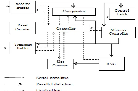
2.2. Block diagram of the Baseband Processor
First at the time of raising edge of the external clock 1, the processor receives serial signals from the RF receive;
these signals may commands or data. Depending on the commands received by the processor, it can performs
different functions like receive data and write into the memory, send data, compare data, kill tag, set/reset tag
and etc.,. The processor enters into HALT mode while it gets bad data or end of the each function. The
processor does nothing when it is in the mode of HALT, then the reset counter starts the count and the processor
resets when the count reaches to 96. To implement the Framed Slotted ALOHA anti-collision algorithm, RNG
and slot counters are used. The baseband processor consists of eight main sub modules. These are receive buffer,
reset counter, transmit buffer, comparator, and controller, slot counter, memory controller and random number
The block diagram of the baseband processor is drawn and shown in fig 2. To improve the efficiency of the
baseband processor, the data flow in between the sub modules has designed as parallel. It can able to improve
the efficiency as significant. The controller plays key role in the processor, it sends control signals to the sub
modules present in the whole processor to control their status. It has to start the sub module and stop it when it
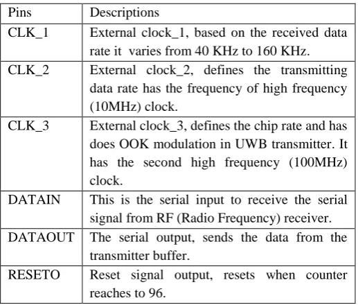
completes its task. It can able to reduce the power consumption to a great level. In table I, pins of the baseband
and description have displayed.
Table I: Pins and Its Desciption of the Baseband Processor
Pins Descriptions
CLK_1 External clock_1, based on the received data
rate it varies from 40 KHz to 160 KHz.
CLK_2 External clock_2, defines the transmitting
data rate has the frequency of high frequency (10MHz) clock.
CLK_3 External clock_3, defines the chip rate and has
does OOK modulation in UWB transmitter. It has the second high frequency (100MHz) clock.
DATAIN This is the serial input to receive the serial
signal from RF (Radio Frequency) receiver. DATAOUT The serial output, sends the data from the
transmitter buffer.
RESETO Reset signal output, resets when counter
reaches to 96.
2.3. Baseband Control Flow
The Framed Slotted ALOHA algorithm is as the anti-collision protocol employed by the baseband processor.
The each tag transmits its ID to the reader in a slot of a frame. The tag is identified by the reader when the
reader receives its ID. The ID can be without collision and the reader sends acknowledgement in the next slot
after receiving the ID. In order to decrease the collision, one special property has arranged that is after the reader
receives an acknowledgement, the identified tag goes to the sleep mode. Collided tags Ids are sends to the next
frame until all the tags are identified.
Table II: Commands Performed By the Processor Depending On the Bits Received
Bit Sequence
Commands and functions
0 Transmitting (data of send ID and CRC)
11 To reset tag
101 Receive data (ID, CRC and Pass data)
1001 Verify data (Send ID, CRC and Pass data)
1000 Checks incoming bit sequence with ID
10001 ACK (Acknowledgement to Set Tag)
100001 Receives Control and writes to the control
Latch
100000 Check incoming bit sequence with Pass
At first, total data contains 64-bit ID, 16-bit CRC, 8-bit Pass, Kill bit and flag bit stored in the memory unit.
Once we switch in the power the processor reads the total data including kill and flag bits. After that, it checks
when it finds the kill bit = 0 i.e., the tag is in active. The RNG continues the process of generation until the
process receives the first 0 bit. Then the process can able to perform the various functions depending on the bits
has received. These functions are tabulated as shown in below Table II.
The state diagram of the baseband process has drawn below in fig 3.
Fig 3: State Diagram of the Baseband Processor
2.4. Sub Modules and Its Description
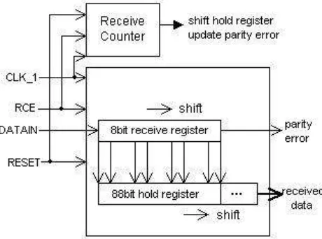
2.4.1 Receive Buffer
To receive the serial data i.e., ID, CRC, Pass and Control; and to check the parity for every 8 bits this buffer is
using. The architecture of this buffer has shown in below figure. It mainly consists of three parts. These are 8-bit
receive register, 88-bit hold register and receive counter. The 8-bit receive register is a 8-bit shift register, at the
time of rising edge of the CLK_1 it right shifts one bit in one shift location. As the same as the 88-bit shift
register i.e., 88-bit hold register can able to right shifts 8-bits at the same edge of CLK_1 i.e., rising edge. The
receiver register starts the operation when it going to receive the data from DATAIN and it sends the data to the
hold register. It shifts the data until total data has to move into the hold register. The RCE is disabled when the
total data has hold in hold register. Then the receiver stops working. The receiver counts the receiving. Already
we know that it has parity checker mechanism. Here it has done when it receives data.
2.4.2 Transmit Buffer
To modulate the data and to send the data, this buffer has used. The architecture of the transmit buffer is shown
in fig 5. It mainly consists of two parts namely 88-bit shift register and transmit counter. Here, the transmitting
cache is analysed by using the synchronous load parallel in-serial out register.
Fig 5: The Architecture Of Transmit Buffer
It has two clock signals i.e., CLK_2 and CLK_3. To transmission purpose, CLK_2 is used and to run the
process of ON/OFF keying modulation, CLK-3 is used. Same as in the receive buffer, here also the 88 bit shift
register has to do the same process and it send the data through the serial shift out. The transmitter counter
counts the transmitting and TRE is disabled when the total data has transmitted. Then the buffer stops working.
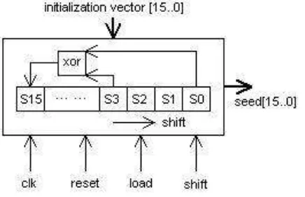
2.4.3 Random Number Generator and Slot Counter
This RNG is using as a 16-bit Linear Feedback Shift Register (LFSR) and the Slot counter is used as a 16-bit
synchronous load down counter. We are proposing a new method to generate the random number, used to
increase the randomness. The architecture of the RNG is shown in fig 6. To determine the initialization vector of
the RNG, we are using the data fetched from the memory i.e., 16-bit CRC data. The functioning period of the
RNG is resolve by using the ID of that tag.
The RNG works later than examination the kill bit and earlier than starting to receive the commands. It works in
the period when the most of modules have free. By this, the peak power of baseband processor can reduce.
The produced 16-bit random number is loaded into the Slot Counter, and the transmission process is awaiting up
to the Slot Counter counts to 0, for that reason different tag can able to transmit in different time slot.
Fig 6: The Architecture of RNG
2.4.4 Memory Controller
The memory controller is an I2C bus controller, while we are choosing I2C bus EEPROM as the memory unit.
CLK_2 is used to clock the memory controller and can able to produce a SCL of 100 KHz. The capability of
EEPROM is 400 KHz but we are using 100 KHz to reduce the power consumption. To connect the I2C bus
controller with the I2C bus we are using tri-state buffers.
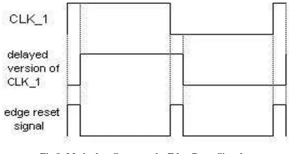
2.4.5 Reset Counter and System Reset Function
The process moves to the HALT mode stays calm when the function has completed or the bad data is entering.
At that moment the Reset Counter begins to count up to 96, and reset the circuit. CLK_2 generates one internal
clock which has 250 KHz used to clock the reset counter and can be reset by the rising and following edge of
the CLK_1. The counter starts the count when the processor enters into the HALT mode if the CLK_1 doesn’t
have rising and following edge.
One short pulse will produce at the output say RESETO to rest the circuit when the count reaches to 96. The
reset counter remains calm when the processor is in work. So, we can understand that it can reduce the power
consumption.
Fig 8: Method to Generate the Edge-Reset Signal
Fig 7 and fig 8 gives the architecture of Rest counter and the generation of reset edge signal respectively.
2.4.6 Controller
The Controller is called the control heart of the baseband processor. It is mostly a FSM; it should be based on
the state diagram of Fig.3. It can able to send control signals to the sub-modules and can also receives status
signals as of the sub-modules to organize their condition. It begins the sub-module when desired and brings to a
close when the sub-module has accomplished its task, this can also reduce the peaking power consumption of
III. SIMULATION AND RESULTS
This paper presents the design of base band processor which will work on the radio frequency identification
scheme. This design will reduce the power required to operate pit. The processor is designed using Verilog HDL
and synthesized in Xilinx ISE 13.2 I.
IV. CONCLUSION
The presented paper shows a novel digital baseband processor for UWB transceiver on RFID. The obtained
results are simulated and synthesized on XILINX tool. No other cryptographic coding is needed for this design
because of the UWB features. In the design, we have used some techniques to reduce the power consumption
V. REFERENCES
[1] Villard, P.; Bour, C.; Dallard, E.; Lattard, D.; de Pontchara, J; Robert, G.; Roux, S.; “A low-voltage
mixed-mode CMOS/SOI integrated circuit for 13.56 MHz RFID applications” SOI Conference, IEEE International
2002 7-10 Oct. 2002 Page(s):163-164.
[2] W. Hirt, “Ultra-wideband radio technology: overview and future research”, Computer Communications,
Vol. 26, pp. 46-52, 2003.
[3] M.B. Nejad, Zhuo Zou, H. Tenhunen, Li-rong Zheng, “A novel passive tag with asymmetric wireless link
for RFID and WSN applications”, To be appeared in proceeding of ISCAS2007 .
[4] R. Howes, A. Williams, M. Evans, “A read/write RFID tag for low cost applications”, RFID Technology
(Ref. No. 1999/123), IEEE Colloquium on 25 Oct. 1999 Page(s): 1/4-4/4.
[5] K. Finkenzeller, “RFID Handbook: Radio-Frequency Identification Fundamentals and Applications”,
Wiley, ISBN: 0471988510.
[6] M. Keating, R. J. Rickford, P. Bricaud, “Reuse Methodology Manual for System-on-a-Chip Designs”,
Springer, ISBN: 1402071418.
[7] M. Zwolinski, “Digital System Design with VHDL”, Prentice Hall, ISBN: 013039985X.
[8] Michael John Sebastian Smith, “Application-Specific Integrated Circuits”, Addison-Wesley Professional, ISBN: 0201500221.
AUTHOR DETAILS
NALLAPU VASANTHA, pursuing her M. Tech (DECS) from Nalanda institute of Engineering and
Technology (NIET), Siddharth Nagar, Kantepudi village, Satenepalli mandal, Guntur Dist., A.P, INDIA. Her
interest in digital communication concepts and is specialized in developing the algorithms.
S. VIDYARANI, has received her M.tech degree and currently working as an Associate professor (VLSI) from
Nalanda institute of Engineering and Technology (NIET), Siddharth Nagar, Kantepudi village, Satenepalli
mandal, Guntur Dist., A.P, INDIA. She has specialized in VLSI backend process and designing different designs