University of Pennsylvania
ScholarlyCommons
Publicly Accessible Penn Dissertations
Fall 12-22-2010
Field Effect and Magnetically Induced Capacitive
Tuning in Hole Doped La1-xSRXMnO3
Zsolt Marton
University of Pennsylvania, [email protected]
Follow this and additional works at:http://repository.upenn.edu/edissertations
Part of theCeramic Materials Commons,Condensed Matter Physics Commons,Nanoscience and Nanotechnology Commons, and theSemiconductor and Optical Materials Commons
This paper is posted at ScholarlyCommons.http://repository.upenn.edu/edissertations/278
For more information, please [email protected].
Recommended Citation
Marton, Zsolt, "Field Effect and Magnetically Induced Capacitive Tuning in Hole Doped La1-xSRXMnO3" (2010).Publicly Accessible Penn Dissertations. 278.
Abstract
Electrostatic modulation of interface conduction between semiconductors and insulating oxides is the foundation of semiconductor technology. This field effect concept can be applied on complex oxides, such as high temperature superconductors and colossal magnetoresistive manganites, in order to create new electronic and magnetic phases. Competition and coexistence of multiple nanoscale phases make them exciting to study around phase transitions. This study on hole doped La1-xSrxMnO3 systems has a two-fold purpose.
One is the demonstration of the field effect on La1-xSrxMnO3 (x = 0.125, 0.2, 0.3, 0.5) thin films. It is an important step towards electrostatic control of material properties; however, a challenging task because of their charge carrier densities of 0.01-1 hole/unit cell, a few orders of magnitude larger than in doped
semiconductors. Control by linear dielectrics needs huge, constantly applied bias. Energy efficient tuning with low voltages requires highly polar ferroelectric. Pb(Zr0.2Ti0.8)O3 was chosen, whose remanence provides 0.5 charge carrier/unit cell on the manganite/ferroelectric interface.
La1-xSrxMnO3/Pb(Zr0.2Ti0.8)O3 heterostructures were synthesized by pulsed laser epitaxy and remarkable conduction modifications were observed in the La1-xSrxMnO3. This can be a strong foundation of a new tool to research electronic oxides.
The second purpose of this work is to utilize the phase separation in manganites. There has been extensive research on multiferroic materials, in which dielectric and magnetic responses are controlled by magnetic and electric field, respectively. In order to demonstrate magnetically tuned capacitance, insulating La7/8Sr1/ 8MnO3 was studied. Drastic capacitance change in magnetic field was shown through a phase transitions and explained in the framework of electronic phase separation. It makes this material eligible for high frequency magnetoelectric applications.
Modulating charge carriers, mobility and magnetism in magnetic oxides, superconductors and superlattices has a great impact on the emerging field of oxide electronics. These compounds overcome the scaling limitations of conventional semiconductors; using low operation voltage oxide ferroelectrics lowers energy consumption. This thesis shows that changing fundamental physical properties of complex oxides on the atomic scale is possible by ferroelectric field effect. This technique is proposed as a tool to study thin films, artificially stacked structures and to induce and optimize novel phases and phenomena.
Degree Type Dissertation
Degree Name
Doctor of Philosophy (PhD)
Graduate Group
Materials Science & Engineering
First Advisor Takeshi Egami
Keywords
manganite, field effect, charge carrier modulation, oxide thin film, pulsed laser epitaxy, oxide electronics
Subject Categories
Ceramic Materials | Condensed Matter Physics | Nanoscience and Nanotechnology | Semiconductor and Optical Materials
CAPACITIVE TUNING IN HOLE DOPED La
1-xSr
xMnO
3Zsolt Marton
A DISSERTATION
in
Materials Science and Engineering
Presented to the Faculties of the University of Pennsylvania
in
Partial Fulfillment of the Requirements for the
Degree of Doctor of Philosophy
2010
Supervisor of Dissertation
________________________
Takeshi Egami Adjunct Professor
Graduate Group Chairperson
________________________
Ju Li
Associate Professor
Dissertation Committee
Charles Graham Professor Emeritus
I-Wei Chen Professor
ii
To my Mother
iii
First of all I would like to express my deepest appreciation to my adviser, Professor
Takeshi Egami, who has always supported me and my research. Valuable conversations
with him lifted me up and kept me going throughout all these years. Thank you for your
patience as well!
Dr. Ho Nyung Lee deserves many thanks for teaching me, among many things, the
essentials of quality oxide film growth, allowing me to work with him.
I would like to give thanks to my dissertation defense committee: Professors I-Wei
Chen ,. Charles Graham and Jay Kikkawa (in alphabethical order), for going through the
program with me and helping me grow an independent researcher.
I am grateful for the Egami group’s members for helpful opinions and the comfortable
atmosphere they provided during my research. I do not want to go “personal” but let me
highlight Dr. Wojtek Dmowski, Dr. Konstantin Lokshin I got to work with on some
projects. Dr. Rinat F. Mamin, visitor scientist with whom I worked on later published
projects, should be mentioned in this section.
My greatest gratitude to Dr. Hans M. Christen and his Thin Films and Nanostructures
Group at Oak Ridge National Laboratory. Let me name some of those with whom I
interacted on a daily basis which meant an incredible emotional support, more than they
would ever think: Dr. Gyula Eres, Dr. Charlee Bennett, Dr. Dae Ho Kim,
Dr. Hyunsik Kim, Dr. Sung-Suk Ambrose Seo, and Dr. Taekjib (TJ) Choi. The
iv
dissertation research, will always have an impact on my scientific growth. As “civilians”
they were always supportive friends outside the lab.
People from other groups in the same Laboratory need to be thanked for scientific
discussions and sometimes more than that: Dr. Brian C. Sales, Dr. Rongying Jin,
Dr.Shiliang Li and Dr. Thomas Zacharia Ward. I got to taste the world of oxide growth
by molecular beam epitaxy, which definitely broadened my knowledge and experience,
even if that work is not included. For this reason I would like to mention here Dr. Rodney
A. McKee as well as Frederick J. Walker. The two years I spent in their lab will always
be remembered.
Now that I am getting more and more emotional while thinking of my support
network, let me dedicate a paragraph to those people who used to shape me as a young
student and will always be a huge part of what I will become in Life: my Hungarian
professors in Debrecen - Dr. Gábor Erdélyi and Dr. Judit Darai - as well as my German
mentor in Kiel – Prof. Dr. Franz Faupel. They realized my eagerness and helped me to
start the quest for an international career.
The gratefullness I owe to the following people is anything but easy to describe.
Long-time friends of mine in no particular order – Tamás Gál, Rita and John Mathew, Cinzia
Metallo, Ferenc Stercel, Gabriella Kornberger, Zohreh Keshavarz and Annamária Nagy –
have seen me falling into the deep and getting back on the horse over and over again for
so many years. I am glad you stayed with me and hope for a way to return the sacrifice.
I appreciate the unmeasurable support, endless and kind conversations, daily coffee
breaks, and Saturday night get-togethers I have got with Lídia & Norbert Podhorszki,
v live, actually.
Sarah Seong Min Wu has stood by me ever since we met and put up with all the issues
I had as well as those she only thought I had, but I really did not :o). She supported me
with unconditional love and without her I would have been bored to death. Here it is,
documented! Mina C, you will always have a special place in my heart.
Last, but certainly not least I thank my Mother, the only person who has been there for
me from the very beginning and never lost faith in me even in the darkest moments. Ever
since I left Hungary, she has been living alone and patiently waiting for me to come and
visit her whenever I am able to. I can just guess how hard it was for her throughout all
these years and I will do everything in my power to ease her life in the future.
Research sponsored by the LDRD Program of ORNL, managed by UT-Battelle, LLC
vi
ABSTRACT
FIELD EFFECT AND MAGNETICALLY INDUCED
CAPACITIVE TUNING IN HOLE DOPED La
1-xSr
xMnO
3Zsolt Marton
Takeshi Egami
Electrostatic modulation of interface conduction between semiconductors and
insulating oxides is the foundation of semiconductor technology. This field effect concept
can be applied on complex oxides, such as high temperature superconductors and
colossal magnetoresistive manganites, in order to create new electronic and magnetic
phases. Competition and coexistence of multiple nanoscale phases make them exciting to
study around phase transitions. This study on hole doped La1-xSrxMnO3 systems has a
two-fold purpose.
One is the demonstration of the field effect on La1-xSrxMnO3 (x = 0.125, 0.2, 0.3,
0.5) thin films. It is an important step towards electrostatic control of material properties,
however, a challenging task because of their charge carrier densities of 0.01-1 hole/unit
cell, a few orders of magnitude larger than in doped semiconductors. Control by linear
dielectrics needs huge, constantly applied bias. Energy efficient tuning with low voltages
requires highly polar ferroelectric. Pb(Zr0.2Ti0.8)O3 was chosen, whose remanence
vii
be a strong foundation of a new tool to research electronic oxides.
The second purpose of this work is to utilize the phase separation in manganites.
There has been extensive research on multiferroic materials, in which dielectric and
magnetic responses are controlled by magnetic and electric field, respectively. In order to
demonstrate magnetically tuned capacitance, insulating La7/8Sr1/8MnO3 was studied.
Drastic capacitance change in magnetic field was shown through a phase transitions and
explained in the framework of electronic phase separation. It makes this material eligible
for high frequency magnetoelectric applications.
Modulating charge carriers, mobility and magnetism in magnetic oxides,
superconductors and superlattices has a great impact on the emerging field of oxide
electronics. These compounds overcome the scaling limitations of conventional
semiconductors; using low operation voltage oxide ferroelectrics lowers energy
consumption. This thesis shows that changing fundamental physical properties of
complex oxides on the atomic scale is possible by ferroelectric field effect. This
technique is proposed as a tool to study thin films, artificially stacked structures and to
viii
Table of Contents
1 Introduction………... 1
References………..………... 6
2 Background………... 8
2.1 Crystal Structure of Manganites………...… 9
2.2 Electronic Structure on Manganites……… 12
2.2.1 The parent compound: LaMnO3………... 12
2.2.2 Jahn-Teller Effect………..13
2.2.3 Exchange Mechanisms………..15
2.2.4 The Phase Diagram of La1−xSrxMnO3………... 21
2.2.5 Electronic Phase Separation……….. 23
2.3 Polarons………... 25
References………..………... 26
3 Methodology…..………. 29
3.1 Substrate Preparation……….. 30
3.2 Thin Film Deposition by Pulsed Laser Deposition (PLD)……….. 32
3.3 Thin Film Characterization………. 38
3.3.1 Structural characterization……… 38
3.3.2 Scanning Probe Microscopy………. 43
3.3.3 Magnetic and Transport Characterization………. 47
3.3.4 Photolithography, Etching and Metallization………... 50
ix
4.2 Pressure Dependent Study……….. 57
4.2.1 Sample Preparation and Crystal Structure……… 57
4.2.2 Magnetism and Electronic Transport……… 59
4.2.3 Conclusions...……… 62
4.3 Reduction by Post-Annealing………. 63
4.3.1 Sample Preparation and Crystal Structure……… 63
4.3.2 Magnetism and Electronic Transport……… 66
4.3.3 Optical Conductivity………. 68
4.3.4 Conclusions………...……… 71
4.4 Growth Control by Laser Fluence………... 71
4.4.1 Sample Preparation and Crystal Structure……… 72
4.4.2 Magnetism and Electronic Transport……… 75
4.4.3 Optical Conductivity………. 81
4.4.4 Conclusions………... 83
4.5 Summary………. 83
References………..………... 85
5 Ferroelectric Field Effect in Manganite Films……… 88
5.1 Introduction………. 88
5.2 Field Effect in Correlated Electron Systems………... 90
5.3 Heterostructure Synthesis………... 98
x
5.4.1 La0.8Sr0.2MnO3 / Pb(Zr0.2Ti0.8)O3 / SrRuO3 / SrTiO3……… 99
5.4.2 La0.8Sr0.2MnO3 / Pb(Zr0.2Ti0.8)O3 / La0.875Sr0.125MnO3 / SrTiO3... 107
5.4.3 La0.8Sr0.2MnO3 / Pb(Zr0.2Ti0.8)O3 / SrTiO3...111
5.5 Summary and Outlook……….120
References………..………. 124
6 Giant Dielectric Permittivity and Magnetocapacitance in La0.875Sr0.125MnO3 Single Crystals………...128
6.1 Introduction………... 128
6.2 Experimental Details………. 130
6.3 Results………... 132
6.4 Discussion………. 135
6.5 Conclusions………... 139
References………..………. 140
xi
Table 1-1 Alternative gate oxides……… 2
Table 3-1 The most common thin film deposition techniques………...……... 33
Table 3-2 X-ray generating anodes with the corresponding wavelengths………. 39
Table 3-3 Atomic force microscopy imaging modes………. 44
xii
List of Illustrations
Figure 1-1 Moore’s Law in terms of device density……… 1
Figure 1-2 Band gap of prospective gate oxides………... 3
Figure 2-3 Angular component of the manganese ionic orbitals……… 13
Figure 2-4 Energy level splitting of 3d electrons………... 15
Figure 2-5 Schematic of the superexchange……….. 17
Figure 2-6 Schematic presentation of the double exchange mechanism………... 19
Figure 2-7 Structural, magnetic and electronic phase diagram of La1-xSrxMnO3……….. 22
Figure 2-8 Electronic phase separation in manganites……….. 24
Figure 3-1 Multiple rocking curve peaks………... 31
Figure 3-2 Basic pulsed laser deposition setup……….. 35
Figure 3-3 Angular dependence of the plume assuming different ablation models…….. 36
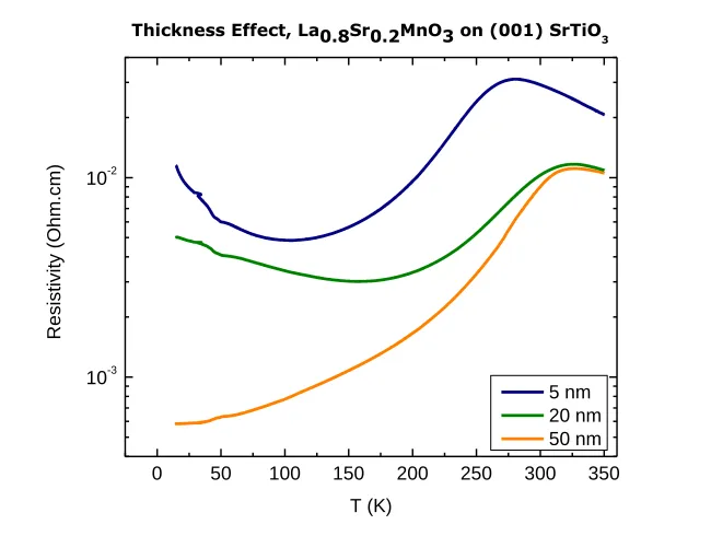
Figure 3-4 Thickness dependence of metal-insulator transition……… 37
Figure 3-5 Illustration of Bragg’s Law in real (a) and reciprocal space (b)……….. 40
Figure 3-6 Illustration of the four-circle diffraction setup……… 41
Figure 3-7 Reciprocal space maps of a thicker and thinner PZT films………. 42
Figure 3-8 Atomic force microscopy operating principles……… 43
Figure 3-9 Atomic force microscopy image of 60nm SrRuO3 on (001) SrTiO3………... 45
Figure 3-10 Basic setup of a piezoforce microscope………. 46
Figure 3-11 The concept of SQUID is based on a pair of Josephson junctions………… 48
Figure 3-12 Metal-insulator transition (MIT) by PPMS and SQUID……… 49
Figure 3-13 Basics of optical photolithography and some examples of devices………... 51
Figure 4-1 LaMnO3 is built of MnO6 corner-sharing and tilted octahedra……….. 56
Figure 4-2 -2 scans on 60 nm LMO films grown in various oxygen pressures………. 58
Figure 4-3 Magnetic transition temperatures of bulk LMO crystals………. 60
Figure 4-4 Magnetic data taken on 60 nm LMO thin films………... 61
Figure 4-5 Synchrotron scattering on the as-grown and annealed LMO………... 65
Figure 4-6 Electronic transport and dc magnetization data on LMO………... 66
Figure 4-7 σ(ω) for the as-grown LaMnO3 films……….….. 68
Figure 4-8 -2 scans of LaMnO3 thin films grown on (001) STO……….. 73
Figure 4-9 In-plane and out-of-plane lattice constants of LaMnO3………... 74
Figure 4-10 Temperature dependence of magnetization of LaMnO3……… 77
Figure 4-11 Critical fluence and Tc dependence on a scattering cross-section…………. 80
Figure 4-12 Optical absorbance spectra taken at room temperature……….. 81
Figure 5-1 Schematic LSMO phase diagram………. 91
Figure 5-2 Transport measurement results on low temperature conductivity…………... 92
Figure 5-3 Square-root type behavior is followed by Ga doped Ge……….. 93
Figure 5-4 The basic structure of a ferroelectric field effect transistor………. 95
Figure 5-5 Field effect works on various correlated electron systems……….. 97
Figure 5-6 Thickness dependent transport and magnetoresistance on thin SRO………. 100
Figure 5-7 Charge carrier sheet density of different correlated………... 101
Figure 5-8 Ferroelectric polarization loops measured at 100 Hz………. 103
Figure 5-9 Calculations in ultra thin BaTiO3………...… 103
xiii
Figure 5-14 Schematics of the PFM experimental setup………. 112 Figure 5-15 Resistivities of LSMO, LSMO/PZT/STO and PZT/LSMO/STO………… 113 Figure 5-16 Resistivities of pure LSMO, LSMO/PZT/STO and PZT/LSMO/STO…… 115 Figure 5-17 Magnetism and electronic transport data on LSMO……… 117 Figure 5-18 Magnetic data as a function of temperature and applied magnetic……….. 118
Figure 5-19 Visualization of doped holes in (La5/8-0.3Pr0.3)Ca3/8MnO3 thin……… 122
Figure 5-20 STO/LAO superlattices of different stacking on (001) NdGaO3…………. 123
Figure 6-1 Temperature dependence of the dielectric permittivity (T)……….. 131
1
1.
Introduction
In the year of 1965, a little while after integrated circuits became booming parts of
applied electronics Gordon Moore made his famous statement (Figure 1-1) that the
number of electronic devices integrated on unit area increased exponentially.1 He
believed this trend to continue leading to dramatic shrinkage in the device dimensions. In
fact, this tendency still holds even today and today’s integrated feature size hit the
sub-micron range. However, microelectronics industry faces a huge problem in following this
trend-line to the future. First, quantum effects in the semiconductor can come into play on
the nanometer scale. Furthermore, the insulation between devices breaks down when
reaching the thickness of a couple of nanometers degrading the circuit’s performance. In
order to overcome this problem, new kind of oxides must be deployed.
Figure 1-1 Moore’s Law in terms of device density
Recent computation technology’s most important parts are random access memories
(RAM). Their basic units are currently memory cells consisting of a field effect transistor
2
used to read out that information. Packing denser such double-element cells onto a silicon
wafer requires smaller lateral dimensions. In order for the capacitors to provide the
essential capacitance, the oxide thickness must be smaller. Eventually, it hits the limit of
a few nanometers beyond which it breaks down, either by quantum mechanical tunneling
or by forming ionic channels. One way to keep up with the same capacitance is to use
high-K insulators so that the thickness does not have to be small.
Prospective high-K insulators for this purpose are oxides such as amorphous HfSixOy,
La2O3, SrTiO3, SrZrO3 or SrHfO3 2,3,4,5,6,7,8. Although the dielectric properties of these
alternative oxides are superior to the conventional ones, they come with new problems.
Table 1-1 Alternative gate oxides from Ref. [9].
Their crystal structure is not compatible with that of silicon. Lattice mismatch defects
CHAPTER 1. INTRODUCTION
3
attempts have been made to engineer good electronic interface between crystalline
perovskite oxide and silicon, the procedure (molecular beam epitaxy) is time-consuming
and requires huge apparatus as well as sophisticated conditions.3 Furthermore, the
mobility in such devices – which determines the reading speed of the memory – is
reported to be below those in commercial ones.4 Other issues, when using linear
dielectrics, are destructive read-out, slowing down of the memory by the refreshing
process, as well as the constant power consumption to keep the memory from
discharging.
Figure 1-2 Band gap of prospective gate oxides as a function of dielectric constant K from Ref. [10].
Switching these dielectrics to ferroelectrics greatly improves the performance of a cell.
First, the reading process is not destructive; it can be done by measuring the channel’s
conducting state. One does not need extra power to keep the bit information when using
long retention time ferroelectric. Writing speed is significantly increased, and reading
4
modern dynamic RAMs of the same feature size. The main goal of the recent FE-RAM
research is to replace 1T/1C structures by 1T configuration. It requires the ferroelectric to
be integrated as a gate oxide. Many attempts have been made to achieve this goal, mostly
by using thin buffer oxides between the PZT and Si to prevent inter-diffusion.11
Another approach is to incorporate perovskite oxide semiconductors, already matching
the new insulators, as metal-oxide-semiconductor field effect transistor (MOSFET)
channels. The idea of doping perovskite transition metal oxides through the field effect
has been around for about four decades. In the early 60’s, ferroelectric oxides were
already used to change the critical temperature of superconductors.12,13,14 Functional
transition metal oxides, such as the high Tc superconductor cuprates and colossal
magnetoresistive manganites, have large charge carrier concentrations of ~1021-1023 cm-3.
To modulate their doping level significantly we need ferroelectrics with huge
polarization, such as Pb(Zr0.2Ti0.8)O3 (PZT). The concentration mentioned above
translates to a polarization of 10-100 μC/cm2.15 It is not easy to reach this upper limit but
some groups are now successful in synthesizing good films,16,17 which may provide
improved electronic interface quality. Since these correlated electron systems show
drastic change in the conduction state by chemical doping, they are promising candidates
for channel materials in ferroelectric memory devices.
Other than the functionality, the concept of field effect offers a flexible and efficient
template to map out material phases, explore fine details and discover new or enhanced
properties in phase transition regimes. Certain bulk materials segregate or decompose,
CHAPTER 1. INTRODUCTION
5
This dissertation focuses on such all-perovskite field effect structures and other
functionalities of manganites, in general. I summarized a set of works, which studied
electronic phase separated single crystalline bulk and thin film manganites. After the
introduction, I give a brief overview on the physics of mixed valent manganites, their
complex but very rich and useful properties in Chapter 2.
Chapter 3 is depicting the experimental facilities and methods I used to carry out the
sample synthesis and characterization of single crystalline thin films. It gives an overview
on pulsed laser epitaxy and several characterization techniques necessary to obtain high
quality samples and results.
Chapter 4 studies numerous pulsed laser ablation parameters and their impact on
material properties via the example of the undoped LaMnO3.This way of starting up was
necessary to get familiar with the sensitivity of thin film quality for the different growth
parameters such as growth pressure, laser energy density on the target etc. The
observation of how important fine-tuning of growth conditions was very important in
synthesizing highly epitaxial single crystalline thin films for field effect studies.
Chapter 5 describes the initial steps I made to demonstrate ferroelectric field effect in
doped manganite thin films, where charge carrier modulation is a real challenge due to
very short screening length. I tried various methods and compositions to overcome this
barrier and partially succeeded in showing significant change in the manganites
electronic and magnetic response presumably caused by field effect. Further experiments
to confirm it are still needed.
6
1
G.E. Moore, Electronics 38 (8), (1965).
2
C. Rossel, B. Mereu, C. Marchiori, D. Caimi, M. Sousa, A. Guiller, H. Siegwart, R.
Germann, J.P. Locquet, J. Fompeyrine, D.J. Webb, C. Dieker, and J.W. Seo, Appl. Phys.
Lett. 89, 053506 (2006).
3
R.A. McKee, F.J. Walker, and M.F. Chrisholm, Phys. Rev. Lett. 81, 3014 (1998).
4
K. Eisenbeiser, J.M. Finder, and Z. Yu, et al., Appl. Phys. Lett. 76 (10), 1324 (2000).
5
G. Wilk and R. Wallace, Appl. Phys. Lett. 74, 2854 (1999).
6
J.Q. He, C.L. Jia, V. Vaithyanathan, D.G. Schlom, J. Schubert, A. Gerber, H.H.
Kolhstedt, and R.H. Wang, J. Appl. Phys. 97, 104921 (2005).
7
B.J. Kennedy C.J. Howard, and B.C. Chakoumakos, Phys. Rev. B 60, 2972 (1999).
8
N. Jin-Aun, N. Sugii, K. Kakushima, P. Ahmet, K. Tsutsui, T. Hattori, and H. Iwai,
IEICE Electronics Express, 3 (13), 316 (2006).
9
J. Robertson, Eur. Phys. J. Appl. Phys. 28, 265–291 (2004).
10
J. Robertson, J. Vac. Sci. Technol. B 18, 1785 (2000).
11
D. Cai, P. Li, S. Zhang, Y. Zhai, A. Ruan, Y. Ou, Y. Chen, and D. Wu Appl. Phys.
Lett. 90, 153513 (2007); T.P. Juan, C. Chang, and Y. Lee, IEEE Electron Device Letters
27 (4), (2006).
12
R.E. Glover and M.D. Sherill, Phys. Rev. Lett. 5, 248 (1960)
13
T.G. Berlincourt, Phys. Lett. 29A, 308 (1969)
14
H.L. Stadler, Phys. Rev. Lett. 14, 979 (1965)
15
C.H. Ahn, A. Bhattacharya, M. Di Ventra, J.N. Eckstein, C. Daniel Frisbie, M.E.
Gershenson, A.M. Goldman, I.H. Inoue, J. Mannhart, A.J. Millis, A.F. Morpurgo, D.
CHAPTER 1. INTRODUCTION
7
16
M. Lisca, L. Pintilie, M. Alexe, and C.M. Teodorescu, Appl. Surf. Sci. 252, 4549
(2006)
17
H.N. Lee, S.M. Nakhmanson, M.F. Chisholm, H.M. Christen, K.M. Rabe, and D.
8
Doped manganites have been known since 1950 through Jonker’s and van Santen’s
work.1 They reported on ferromagnetism in chemically mixed crystals of LaMnO3
-CaMnO3, LaMnO3-SrMnO3 and LaMnO3-BaMnO3. This discovery led to numerous
experimental studies which led to the observation of a rich list of coexisting magnetic and
electronic phases in La1-xCaxMnO3 and La1-xSrxMnO3 in the entire doping level range.2
Later theoretical works tried to explain these unusual phenomena by introducing the
concept of double exchange by Zener3, as well as Anderson and Hasegawa4, de Gennes.5
Recently these materials have become the focus of intense research activities because
of reasons related to possible applications. External magnetic field influences the
electronic transport properties of most perovskite manganites. In certain doping and
temperature ranges, they exhibit colossal magnetoresistive (CMR) behavior: in applied
magnetic field the electronic resistivity changes by orders of magnitude, because
magnetic order seems to enhance conductivity. Furthermore, the CMR compounds
undergo a metal-to-insulator transition, which is a quite broad transition and will be
discussed later in terms of percolation theory.
Very large CMR constants were found in epitaxial thin films of chemically doped
manganites at room temperature, which also boosted active research on these materials.6
It makes them very attractive for industrial applications except that the CMR has to occur
at room temperature where magnetic detection is needed, whereas it is observed at the
CHAPTER 2. BACKGROUND
9
A clear and unified explanation of physical mechanisms leading to CMR effect has not
been given yet. One of the best descriptions recently proposed is based on nano- or
micron scale electronic phase separation. This picture involves the coexistence of at least
two different magnetic/electronic phases, such as paramagnetic insulator and
ferromagnetic metallic. Their competition and percolation determines the basic properties
of the compound.7,8,9,10,11,12,13 An exact physical picture of these physical phenomena
would be applicable onto other systems, such as high temperature superconductors,
where electron correlations and strong interactions between charge, spin, orbital and
lattice degrees of freedom play a significant role.14 The other phenomenon making
manganites fascinating is the almost complete spin polarization in the CMR composition
range.15
In this chapter I am giving a brief introduction on structural, magnetic and electronic
properties of manganites in general as well as the most contemporary description to
explain the physics behind the rich phase diagrams. Since it is a quite broad topic and
cannot be fully covered in this chapter, to learn more about correlated electron systems
the reader is advised to consult extensive reviews available today.16,17,18,19,20
2.1
Crystal Structure of Manganites
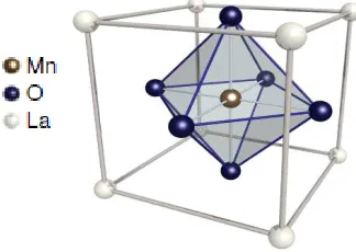
Manganites of chemical formula of AMnO3 form lattices, which are mostly slightly
modified perovskite structures (Figure 2-1). The A cation, which is Lanthanum in our
case, is located in the corners of a cube, while the manganese ion is surrounded by an
oxygen octahedron. These octahedra are usually sharing corners in the manganites this
10
Figure 2-1 Cubic perovskite structure of AMnO3 manganates.
These octahedra can undergo Jahn-Teller distortion, which perturb relative orientations of
electronic orbitals as well as the octahedra themselves. This way the lattice structure can
change from cubic to orthorhombic or rhombohedral. This perturbation in the crystal
structure is related to the sizes of the ions, and can be characterized through the tolerance
factor defined like this:
O A
O Mn
r r
r r f
2 1
(2-1)
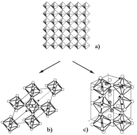
The tolerance factor determines the crystal structure in doped manganites as explained
in Figure 2-2.
For tolerance factor 1 we get a perfect cubic lattice with a Mn-O-Mn bond angle of
180º. When lowering f, the structure turns into rhombohedral. Tilting the octahedral also
leads to bending Mn-O-Mn bond angle, which plays a huge role in resulting magnetism
CHAPTER 2. BACKGROUND
11
Figure 2-2 Crystal structure for different tolerance factors. (a) Simple cubic in case there is no
distortion present in the crystal. For 0.96 < f < 1.00 the resulting crystal structure is rhombohedral
(b), while f < 0.96 gives orthorhombic lattice (adopted from Ref.[16]).
The tolerance factor can be easily changed by chemical doping. It has a great impact
on manganites’ physics. The normally La3+
ions are replaced by divalent ions such as
Ca2+, Ba2+ or Sr2+. The doping ions have different ionic radii influencing the tolerance
factor and so magnetic and electronic properties of the mixed valence systems. The lattice
distortion induced by doping is relatively small in the case of manganites under study in
this work, so I normally used the pseudo-cubic nomenclature for structural
12
2.2
Electronic Structure on Manganites
2.2.1
The parent compound: LaMnO
3In order to understand the electronic and magnetic correlation along the entire mixed
valent phase diagram, the parent compound needs fundamental understanding.
Lanthanum ions form a rather strong bond with the oxygen ions in the La-O plane due to
the huge electron affinity of the O2- species. That is why they can be treated as inert
spacer between the MnO6 octahedra and in most cases the La-O planes are irrelevant
when considering the electronic structure or magnetism in mixed valent manganites.
In the undoped composition, manganese ions have the [Ar]3d4 structure resulting in
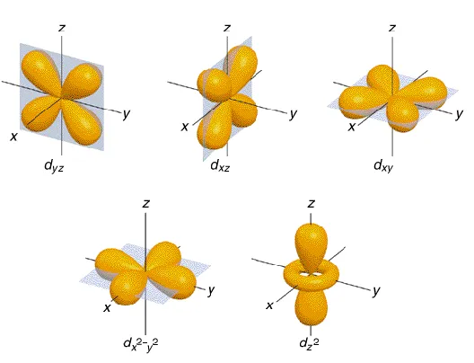
Mn3+ valence. Without any ligand shell around it, the Mn3+ ion has one electron and five
degenerate orbital states available (see Figure 2-3). As soon as it is surrounded by an
oxygen octahedron, the electrostatic field of the oxygen ions, so-called crystal field, splits
the degenerate states of the d electron. There are three lower energy degenerate orbitals
called t2g (dxy, dxz, dyz) pointing in-between the oxygen p orbitals, while the remaining two
higher energy orbitals (eg) have direct overlap with the oxygen 2p ones. They are marked
as dz2-r2 and dx2-y2. The energy difference is easy to understand, since the two eg orbitals
face the oxygen electronic orbitals and feel the strong Coulombic repulsion, making it
less desirable for electron on the manganese site. The energy difference between the t2g
and eg states is called the crystal field splitting energy (CF = 10Dq) and is about the
order of 1eV.16 The on-site Hund’s coupling energy, on the other hand, is more than the
CHAPTER 2. BACKGROUND
13
electrons and the eg electron and eventually spin polarized eg electrons mentioned above.
The situation is schematically shown later by Figure 2-4.
2.2.2
Jahn-Teller Effect
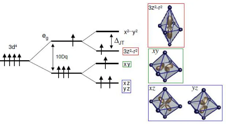
If an eg orbital is occupied by an electron, we observe a fascinating phenomenon
called Jahn-Teller distortion or effect. The degenerate 3d orbitals split when put in a
crystal field. In the case of octahedral coordination, the one orbital pointing to the
z-direction (dz2-r2) will be the lower energy choice. As soon as the electron occupies that
orbital, the eg electron interacts with the oxygen 2pz electrons and pushes the upper and
displaces the upper and lower oxygen ion like depicted in Figure 2-4. This way the
Coulombic energy is lowered by building up a strain field. This is called the Jahn-Teller
distortion.
14
The effect also influences the t2g levels because of obvious symmetry breaking
reasons. dxz and dyz levels have the same energy but lower than in the case of undisturbed
3d ion, while the dxy orbital is getting higher in terms of energy, since the oxygen ions in
the xy plane are getting closer. Interesting fact, though, that the net energy of the
Jahn-Teller distorted orbital configuration does not change.21
The resulting strain field cooperatively distorts the whole lattice. The distorted
octahedral self-organize in the xy plane in a zigzag way. This collective Jahn-Teller effect
can give rise to either rhombohedral or orthorhombic structure. This strongly localized
strain field realized by purely electronic reasons is called a Jahn-Teller polaron.22 The
explanation of the strong localization is easy to see. Once the eg electron wants to hop to
a neighboring site, the whole strain field has to be displaced, which costs tremendous
amount of energy.
It can be seen, that as soon as we dope the parent compound by 2+ valence ions, we
dope holes in the system and destroy the eg electrons as and the Jahn-Teller polaron. The
doped holes become delocalized as a result of missing strain field trapping them. Doping
CHAPTER 2. BACKGROUND
15
Figure 2-4 Energy level splitting of 3d electrons due to octahedral crystal field and Jahn-Teller
distortion.
2.2.3
Exchange Mechanisms
The parent LaMnO3 is an antiferromagnetic insulator below the Néel temperature of
about 140K. Above that it is paramagnetic. Ferromagnetic correlations can be induced by
chemical doping. When doping, the electron stoichiometry looks like this
2 3 4 3 1 2 3
1 Sr Mn Mn O
La x x x x (2-2)
The mixed valence feature has a great influence on magnetic and electronic conductive
properties of manganites, as mentioned before. After about 8 percent hole doping
ferromagnetic correlations set in and beyond x = 0.17 electronic conduction starts. To
qualitatively explain the rich phase diagram of doped manganites, the concept of
superexchange and double exchange needs introducing. Well detailed and quantitative
16
In order to explain the magnetic structure, we only need to consider the spin
alignments on the manganese ions. La3+, Sr2+ and O2- have the noble gas configuration
and that is why they exhibit no magnetic moment. Also, 3d transition metals in cubic
environment display zero net orbital moment. As a consequence, it is enough to discuss
the spin moments on the manganese ions to describe magnetism. These are composed of
S(Mn3+) = 2 and S(Mn4+) = 3/2.
For electronic conduction, only the eg electrons count since the t2g levels are way
below the Fermi level and they are strongly localized due to the crystal field splitting.
Indirect superexchange and double exchange interactions are necessary to explain the
magnetic correlations and conductions states in mixed valent manganites. Since the
manganese ions are fairly far away from each other, the oxygen 2p orbitals are necessary
to involve in the description. During the electronic transport the spins of the conduction
electrons are to be kept unchanged since spin flipping is energetically not favorable.
2.2.3.1
Superexchange
Superexchange models direct exchange interaction between Mn3+ ions disregarding
the O2- in between. In this picture kinetic energy, characterized by the hopping amplitude
t > 0 and potential energy (U) are used. The hopping integral says how delocalized the
electron is, while U > 0 is the Coulombic energy mostly depicting the repulsion between
two on-site electrons.
The superexchange relation can be derived from second order perturbation theory 21,
CHAPTER 2. BACKGROUND
17
U t J
2
(2-3)
Qualitatively, the oxygen ions can be disregarded, when discussing the superexchange
interaction (Figure 2-5). Two neighboring dz2-r2 orbitals pointing toward each other are
considered. The degenerate nature is already assumed due to Jahn-Teller effect. In case
the eg electrons’ spin orientation is antiparallel, then virtual hopping is forbidden by the
Pauli principle, so there is no energy gain. However, when spins are aligned parallel,
virtual hopping can occur and energy is gained via delocalization. It comes with
antiferromagnetic correlation due to strong Hund’s coupling to the t2g electrons on the
manganese ion the electron hops onto.
Figure 2-5 Schematic of the superexchange relation between two non-degenerate dz2-r2 orbitals with
parallel (a) and antiparallel (b) spin orientation.
Superexchange is, on the other hand, a really simple description and often not enough
to explain certain phenomena. A much more refined picture is provided by the so-called
Goodenough-Kanamori-Anderson (GKA) rules.24,25 It takes into account several orbital
18
easy-to-understand explanation for the parent compounds on both ends of the LaMnO3
-SrMnO3 phase diagram.
Applying these rules, one can easily explain the observed ferromagnetic coupling in
the ab plane of LaMnO3 as well as the out-of-plane anti-ferromagnetic interaction
(A-type antiferromagnet). The same way can be explained the G-(A-type anti-ferromagnetism in
SrMnO3, where every single neighboring manganese ion is anti-ferromagnetically
coupled to each other.
2.2.3.2
Double Exchange
When holes are introduced in the system by replacing La ions by Sr/Ca ions, the
magnetic interaction can be well described by the double exchange model. It explains the
appearance of ferromagnetism and the delocalization/conduction in doped compounds.
It also provides with a simple but effective explanation on how negative colossal
magnetoresistance occurs in certain composition regions.
The setup is very similar to that of the superexchange; however one starts out with
different valences: Mn4+-O-Mn3+. This fact clearly influences the hopping process, since
there is no repulsing on-site Coulombic interaction on the other ion. Now all the energy
terms should be taken into account.
The first I discuss is, where there is an eg electron on a Mn3+, whose spin is aligned
with the t2g spins. It can hop via the oxygen and arrive in an unoccupied eg orbital if the
CHAPTER 2. BACKGROUND
19
it net energy by the kinetic energy amount due to delocalization and also the lack of
on-site Coulombic interaction favors this exchange.
Figure 2-6 Schematic presentation of the double exchange mechanism. In the case of parallel core
spin alignment (a), electrons can hop between Mn ions via the O2-2p orbital. However, antiparallel
spins lead to localization (b).
Figure 2-6(b) shows the other possibility, when the Mn4+t2g spins are aligned antiparallel
with respect to those of the Mn3+. If the electron wanted to hop onto the neighboring Mn
site, it should overcome a relatively large Hund’s coupling energy. It is plain to see, that
in a mixed valent situation ferromagnetic and delocalized states are energetically
favorable and they eventually win over the localized anti-ferromagnetic order. It explains
the ferromagnetic metallic phase observed at certain doping levels in CMR manganites.
So one can see that the eg electrons form a band, whose width W is proportional to the
hopping integral t.22
From the double exchange model comes a really fascinating consequence. Since the
delocalized electron interacts with the t2g electrons via Hund’s coupling, the conduction
electrons turn out to be 100% spin polarized in the ground state. This was also confirmed
20
In case one is curious about thermal excitation, the hopping integral t becomes a
function of the angle ij between the nearest neighbor core spins.
2
ij eff t
t (2-4)
As it shows, a maximum conduction is gained when the core spins are
ferromagnetically aligned, while ideally zero, if the spins are antiparallel. At higher
temperatures, upon heating, the spins are randomly aligned due to thermal excitations.
This way the ferromagnetism as well as good electric conduction is suppressed. This
metal-to-insulator transition occurs at the Curie temperature; however it is a quite broad
transition on the temperature scale (a couple of tens of degrees). In this context, colossal
magnetoresistance can be explained by a fairly simple picture. An external magnetic field
forces local spins to align parallel to the external field and so increase the electron
hopping integral, i.e. conductivity, due to the double exchange mechanism. Since at low
temperature the spins are already aligned ferromagnetically, an external field does not
have a huge effect, ergo the magnetoresistance is lower. In the transition region, the
material is in a critical state, where ferromagnetism is all over the crystal, but no
percolation happens. Percolation is triggered by external magnetic field, which suddenly
flips the conduction state into metallic and so leads to insulator-to-metal transition. At
higher temperature the external field is not enough to overcome the thermal excitations,
CHAPTER 2. BACKGROUND
21
Even if the double exchange mechanism describes the correlation between magnetism
and electric conductivity very well, it has limitations, which should be resolved by
introducing a further concept of electronic phase separation.
2.2.4
The Phase Diagram of La
1−xSr
xMnO
3This subsection will introduce the fairly rich phase diagram of La1-xSrxMnO3 (see
Figure 2-7). The parent compound, LaMnO3, is an A-type antiferromagnetic insulator
below its Néel temperature of around 140K. It has orbital ordered, ferromagnetically
coupled ab planes coupled antiferromagnetically to the neighboring ab planes. It can be
described by the superexchange interaction discussed above.
When doped, a low temperature ferromagnetic but insulating phase sets in above x ~
0.1 doping level. This phase, which survives up to x ~ 0.17, cannot be modeled by a
simple double exchange interaction, since electronic conduction starts only above x =
0.17 despite the ferromagnetic correlation. This magnetic-electronic switching is
22
Figure 2-7 Part of the rich structural, magnetic and electronic phase diagram of La1-xSrxMnO3 on the
lanthanum rich side (x 0.5). Orthorhombic (O) and rhombohedral (R) crystal structures serve as
lattice basis for A-type antiferromagnetic and ferromagnetic insulator (AFI/FI), ferromagnetic
metallic (FM) as well as high temperature paramagnetic insulator(PI) and metallic (PM) phases [16].
After the critical 0.17 doping, Tc increases monotonically to 370K at x = 0.3.
Apparently, the number of Mn4+ ions grows and it lets the double exchange win over
superexchange. On the other hand, this low T ferromagnetic insulator-to-metal transition
coincides with a structural transition, so the abrupt change in the tolerance factor cannot
be excluded from the possible explanations.
Even if most parts of the phase diagram can be explained by the competition between
the two exchange mechanisms, some regions are still puzzling and cannot be fitted into
this schematic picture. Such question is why the CMR effect peaks in the rhombohedral
FM region at that particular doping, and not in the tetragonal range, where the doping is
even more and it is still FM.19 Obviously, the exchange mechanisms promoted above are
CHAPTER 2. BACKGROUND
23
behaviors at doping levels x > 0.5. Also paramagnetic insulator states were detected in the
FM doping region. There was transition temperature shift of about 20K observed due to
isotope-effect in La0.8Ca0.2MnO3+y, when 18O replaced the conventional oxygen isotope.26
In the following, the model of electronic phase separation will be introduced, which
will become relevant to explain certain experimental results in this thesis later such as
colossal magnetocapacitance in low doped manganite single crystals and the possibly
larger screening length in high charge carrier density LSMO films.
2.2.5
Electronic Phase Separation
In order to explain colossal magnetoresistance in electronically homogeneous doped
manganites seems to be impossible. Explanations of CMR based on pure exchange
mechanisms and Anderson localization, as well as the paramagnetic insulator state
described only by a gas of small polarons 27 should be further developed.
The missing part of the puzzle is the concept of electronic phase separation. In this
picture, coexistence and competition of two or more electronic and magnetic phases is
assumed. The size clusters of different electronic/magnetic nature is mostly on the
nanoscale 28, but can be even larger 29.
This model allows us to understand the phase diagram as well as the CMR effect 30
and is in good agreement with numerous experimental observations.7,8,9,10 That is why
scanning probe microscopy studies find regions with different conductivity under the
transition temperature, whose relative fractions can be varied by external magnetic field.
24
formation of a new phase upon cooling or applied magnetic field, such as metal-insulator
transition.
Electronic phase separation (see Figure 2-8) plays an important role in comprehending
not only manganites, but other correlated electron systems, such as high temperature
superconductivity.27 Nice reviews on this picture can be found in Ref. [31] and Ref. [27],
for example.
Figure 2-8 Electronic phase separation in manganites has been observed by several experimental
techniques, like scanning electron nano-diffraction (a), for example [28]. (b) This schematic concept
is a powerful tool for theoreticians as well [14] to study material properties of correlated electron
systems.
(a) (b)
CHAPTER 2. BACKGROUND
25
2.3
Polarons
Polarons are immobile electrons with the strain field they create around themselves.22
Polarons were always neglected when considering the metallic ground states of
manganites, since the mixed valent nature and the double exchange mechanism ensures
complete delocalization and polarons entirely disappear.16 However, above a certain Tc
polarons form again, and charge carriers form Jahn-Teller distortion, become localized
due to the polaron’s very high ~ 1 eV binding energy.
This effect is especially important for polaron hopping driven transport in narrow band
gap manganites like La1-xCaxMnO3 or Pr1-xCaxMnO3.32 Some experiments show that
polarons in metallic phases are not to neglect. For instance in charge ordered
compositions, like La0.75Ca0.25MnO3 in Ref. [33], which are free of elastic stress and
electronically completely homogeneous. Even in such a homogenous form they show a
big CMR effect.34 It means that in these cases, even electronic phase separation is not
satisfactory to explain the materials behavior. The important role played by polarons
were demonstrated through anisotropic charge density wave measurements done below
and above the Curie temperature of x = ¼ charge ordered composition.33 These
experiments show that polaronic effects are not only relevant for the high temperature
paramagnetic insulating states but also in the metallic phases. A quite wide overview is
26
References
1
G.H. Jonker and J.H. van Santen, Physica XVI, 599 (1950).
2
E. Wollan and W. Koehler, Phys. Rev. 100, 545 (1955).
3
C. Zener, Phys. Rev. 82, 403 (1951).
4
P.W. Anderson and H. Hasegawa, Phys. Rev. 100, 675 (1955).
5
P.-G. de Gennes, Phys. Rev. 118, 141 (1960).
6
R. von Helmolt, J. Wecker, B. Holzapfel, L. Schultz and K. Samwer, Phys. Rev. Lett.
71, 2331 (1993).
7
T. Becker, C. Streng, Y. Luo, V. Moshnyaga, B. Damaschke, N. Shannon and K.
Samwer, Phys. Rev. Lett. 89, 237203 (2002).
8
M. Fäth, S. Freisem, A.A. Menovsky, Y. Tomioka, J. Aarts and J. A. Mydosh, Science
285, 1540 (1999).
9
M. Uehara, S. Mori, C.H. Chen and S.-W. Cheong, Nature 399, 560 (1999).
10
Ch. Renner, G. Aeppli, B.-G. Kim, Yeong-Ah Soh and S.-W. Cheong, Nature 416, 518
(2002).
11
S. Yunoki, A. Moreo and E. Dagotto, Phys. Rev. Lett. 81, 5612 (1998).
12
M. Mayr, A. Moreo, J.A. Vergés, J. Arispe, A. Feiguin and E. Dagotto, Phys. Rev.
Lett. 86, 135 (2001).
13
J. Burgy, M. Mayr, V. Martin-Mayor, A. Moreo and E. Dagotto, Phys. Rev. Lett.
87, 277202 (2001).
14
CHAPTER 2. BACKGROUND
27
15
J.-H. Park, E. Vescovo, H.-J. Kim, C. Kwon, R. Ramesh and T. Venkatesan, Nature
392, 794 (1998)
16
Y. Tokura, Colossal Magnetoresistive Oxides (Advances in Condensed Matter
Science), Gordon and Breach Science Publishers, (2000).
17
J.M.D. Coey, M. Viret and S. v. Molnár,Adv. Phys. 48, 167 (1999).
18
E. Dagotto, Nanoscale Phase Separation and Colossal Magnetoresistance, Springer
Verlag, Berlin (2002).
19
E. Dagotto, T. Hotta and A. Moreo, Phys. Rep. 344, 1 (2001).
20
V. Moshnyaga and K. Samwer, Handbook of magnetism and advanced magnetic
materials, Volume 5: Spintronics and magnetoelectronics, John Wiley & sons (2007).
21
S. Blundell, Magnetism in Condensed Matter, Oxford University Press, (2003).
22
Ch. Kittel, Introduction to Solid State Physics, (2004).
23
J.B. Goodenough, Phys. Rev. 100, 564 (1955).
24
J.B. Goodenough, Magnetism and Chemical Bonds, Interscience Publishers, New
York (1963).
25
D.I. Khomskii and G.A. Sawatzky, Sol. State Comm. 102, 87 (1997).
26
G.-M. Zhao, K. Conder, H. Keller, K.H. Müller, Nature 381, 676 (1996).
27
E. Dagotto, New Journal of Physics 7, 67 (2005).
28
J. Tao, D. Niebieskikwiat, M. Varela, W. Luo, M. A. Schofield, Y. Zhu, M. B.
Salamon, J. M. Zuo, S. T. Pantelides, and S. J. Pennycook, Phys. Rev. Lett. 103, 097202
(2009).
29
T. Z. Ward, J. D. Budai, Z. Gai, J. Z. Tischler, Lifeng Yin and J. Shen, Nature Physics
28
30
A. Moreo, S. Yunoki and E. Dagotto, Science 283, 2034 (1999).
31
N. Mathur and P. Littlewood, Physics Today 56, 25 (2003).
32
W. Westhäuser, S. Schramm, J. Hoffmann and Ch. Jooss, Eur. Phy. J. B 53, 323
(2006).
33
L. Sudheendra, V. Moshnyaga, E. D. Mishina, B. Damaschke, Th. Rasing and K.
Samwer, Phys. Rev. B 75, 172407 (2007).
34
V. Moshnyaga, L. Sudheendra, O. I. Lebedev, S. A. Köster, K. Gehrke, O. Shapoval,
A. Belenchuk, B. Damaschke, G. van Tendeloo and K. Samwer, Phys. Rev. Lett. 97,
107205 (2006).
35
29
3.
Methodology
All the oxide thin films in this dissertation were synthesized on atomically flat (001)
SrTiO3 and NdGaO3 substrates by pulsed laser deposition. This chapter presents the
substrate preparation. Most of the samples went through a set of basic characterization
methods which will be introduced here as well. High resolution (minimum step size
0.0001°) four-circle X-ray diffraction was used to measure thickness by X-ray
reflectivity, in- and out of plane lattice constants which were translated into strain.
Rocking curves on substrate and film peaks delivered information about the degree of
crystallinity. Atomic force microscopy verified surface roughness or possibly the growth
mode (island, layer-by-layer) of the oxide layers. Piezoresponse force microscope, a
modified AFM, was used to image ferroelectric polarization.
Depending on the purpose of the samples, they underwent magnetic measurements as
a function of temperature and applied magnetic field in a superconducting quantum
interference device. Electronic transport properties were investigated by a physical
properties measurement system. In order to do the electric characterization, usually
device structures needed patterning by photolithography and etching, putting metallic
contacts onto samples by radio frequency (RF) sputtering (Pt electrodes), e-beam or
thermal evaporation (Cr/Ti + Au).
3.1
Substrate Preparation
One of the most frequently used substrates in this dissertation was (001) oriented
30
CrysTec GmbH or Sinkosha Co., Ltd. (miscut tolerance < 0.05°, grown by the Verneuil
process). Its cubic lattice constant a = 3.905 Å is close to most of the thin films’ I grew.
However one needs to keep in mind that STO undergoes a structural phase transition at
around 105 K. It sometimes showed up in electronic transport measurement as a small
kink.
STO is a series of SrO and TiO2 atomic planes. As received, the STO substrate
surfaces are quite rough (because of rough polishing agent grain size) and chemically
disordered due to SrO segregation.1 The chemically mixed and uneven surface needed to
be flat and single terminated in order to keep good mechanical and chemical interface
properties. The single TiO2 terminated, atomically flat STO surfaces were prepared
according to Ref. [2]. The substrates were etched in 1:10 aqueous solution of NH4F
buffered HF for 30seconds. This process is supposed to etch away the excess SrO from
the surface. Then they were rinsed in flowing de-ionized water for about 1 minute and
dried by pure, pressurized N2 gas flow. A typical annealing process takes 1 hour at
1050-1100C in air. This process offers quite reproducible results on substrate slides cut from
the same STO wafer; however it often happens that the preparation procedure needs to be
altered depending on preliminary surface images, as Figure 3-1 depicts.
Besides surface quality, crystallinity of the substrates has a big influence on the thin
film growth. One has to ensure that mosaicity (the rocking angle, in degrees, in both the
vertical and the horizontal directions) is kept as low as possible. I inspected every single
substrate by X-ray diffraction, e.g. rocking curve scans (see section 3.3.1 for more
CHAPTER 3. METHODOLOGY
31
Figure 3-1 Multiple rocking curve peaks imply bad [blue line on (a)] while single ones good [both
lines on (b)] crystallinity. The rocking curve scans were taken on STO (002) peak at the azimuth
angle = 0° (red) and = 90° (blue). Atomic force microscope (see section 3.3.2) images (5μm 5μm)
were recorded on previously etched then annealed (c) and re-annealed (d) substrates. The latter
showed improvement in surface quality.
21 .0 21 .5 22 .0 22 .5 23 .0 23 .5 24 .0 2 4.5 2 5.0 2 5.5
Ome ga (°)
0 .1 2 3 5 1 2 3 5 1 0 2 3 5 10 0 2 3 5 1 00 0 2 3 5 In te ns ity (c o un ts )
21 .0 2 1.5 2 2.0 22 .5 23 .0 2 3.5 2 4.0 24 .5 2 5 .0 2 5.5
Ome ga (°)
0 .1 2 5 1 2 5 1 0 2 5 10 0 2 5 1 00 0 2 5 10 00 0 2 5 1 00 00 0 2 5 In te ns ity (c o un ts ) 1150C/1h a) b) c) d)
21 22 23 24 25
10-1 100 101 102 103 104 105 106 In te n s it y ( a rb it ra ry u n it s )
2 (degrees) (b)
21 22 23 24 25
100 101 102 103 104 (a) In te n s it y ( a rb it ra ry u n it s )
2 (degrees)
21 .0 21 .5 22 .0 22 .5 23 .0 23 .5 24 .0 2 4.5 2 5.0 2 5.5
Ome ga (°)
0 .1 2 3 5 1 2 3 5 1 0 2 3 5 10 0 2 3 5 1 00 0 2 3 5 In te ns ity (c o un ts )
21 .0 2 1.5 2 2.0 22 .5 23 .0 2 3.5 2 4.0 24 .5 2 5 .0 2 5.5
Ome ga (°)
0 .1 2 5 1 2 5 1 0 2 5 10 0 2 5 1 00 0 2 5 10 00 0 2 5 1 00 00 0 2 5 In te ns ity (c o un ts ) 1150C/1h a) b) c) d)
21 22 23 24 25
10-1 100 101 102 103 104 105 106 In te n s it y ( a rb it ra ry u n it s )
2 (degrees) (b)
21 22 23 24 25
100 101 102 103 104 (a) In te n s it y ( a rb it ra ry u n it s )
32
3.2
Thin Film Deposition by Pulsed Laser Deposition (PLD)
Thin film form of materials has been the subject of intriguing research for almost a
half of a century. Integrated circuit technology boosted interest in inventing and
developing thin film deposition techniques which provide us with high crystalline quality
thin films on numerous substrates. Large scale and highly cost effective deposition
techniques are mainly used by academic research as well as private sector R&D
departments.
There are various methods out there aiming at supplying thin layers of materials. The
most widely used are thermal and electron-beam (E-beam) evaporation, sputtering
techniques, plasma-enhanced and low pressure chemical vapor deposition (PECVD,
LPCVD), molecular beam epitaxy (MBE) and pulsed laser deposition Table 3.1. In this
doctoral research, I used pulsed laser deposition as the tool to produce superior crystalline
quality functional oxide thin films, heterostructures, and multilayers on various oxide
substrates. This method is quite versatile: many materials can be grown in a number of
background gases and pressures. It is a fast, clean, highly energetic (eV) and relatively
inexpensive growth technique. In addition, it is easily scalable for potential mass
CHAPTER 3. METHODOLOGY
33
Table 3.1 The most common thin film deposition techniques and their typical parameters.
Process
Material Grain Size Deposition
Rate
Substrate
Temperature
Cost
Thermal
evaporation
Metals / low melting
point materials
10-100 nm 1-20 Å/s 50-100 ˚C Very low
E-beam
Evaporation
Metals / dielectrics 10-100 nm 10—100 Å/s 50-100 ˚C High
Sputtering Metals / dielectrics ~ 10 nm 1-100 Å/s ~ 200 ˚C High
PECVD Dielectrics 10-100 nm 10-100 Å/s 200-300 ˚C Very high
LPCVD Dielectrics 1-10 nm 10-100 Å/s 600-1200 ˚C Very high
MBE Metals / dielectrics 1nm- 1 cm 1-10 ML*/min 600-1000 ˚C Very High
PLD Metals / dielectrics 1 nm–1 cm 0.5-50 ML*/s 500-800 ˚C Low
*ML stands for monolayer
PLD has been around for quite some years. It is one of the leading techniques to
deposit highly epitaxial thin films. After Albert Einstein proposed the concept of
stimulated emission, it took more than 40 years to construct the first optical maser
utilizing ruby at that time. Early works on laser-solid interactions3 resulted in the first
solid thin film depositions in 1965.4 The initial films grown by PLD did not produce
significant break-through, since they were inferior to those obtained via other deposition
techniques, such as chemical vapor deposition (CVD) or molecular beam epitaxy (MBE).
After about twenty years PLD was used to grow the first film of the new high
temperature superconducting material YBa2Cu3O7+ (YBCO).5 This event started the
renaissance of PLD. Ever since, high quality metallic, ceramic oxide and oxide
multilayers (for a review see for example Ref. [6]), nitride films as well as carbon
34
In a nutshell, PLD basically shines energetic and focused laser beam onto a target
material which has exactly the composition as the demanded thin layer (for a nice review
see [8]). The substrate is mounted on a heater facing the target. As the laser pulses hit the
target, the ablated material flies onto the pre-heated substrate and crystallizes (Figure
3-2). In the case of oxide deposition, the cation stoichiometry is often secured by the
target; however oxygen has to be supplied externally. PLD is extremely sensitive to many
growth parameters such as laser energy density on the target (later referred to as
fluence)9, growth pressure, background gas, substrate temperature, target-substrate
distance, even the oxygen flow’s direction and relative position with respect to the target.
The basic setup of our PLD station starts out with a KrF (λ = 248 nm) excimer laser. It
is guided to the deposition chamber by using different laser lenses and mirrors. Where the
actual growth happens is a relatively small vacuum chamber with a quartz viewport on
one side allowing the laser beam to penetrate, since its transmission at this wavelength is
about 90-95%10 and it is transparent in the visible range as well. A rotating carousel
accommodates a maximum of 4 target holders. This feature allows us quick ability to
switch between targets and so to create heterostructures, superlattices or simply mix
multiple materials like a (quasi) co-deposition. Most of the substrates I used are
5mm×5mm which is small enough to keep the film thickness uniform as far as the
![Table 1-1 Alternative gate oxides from Ref. [9].](https://thumb-us.123doks.com/thumbv2/123dok_us/9259111.1463981/18.612.129.517.351.629/table-alternative-gate-oxides-ref.webp)

![Figure 3-1 Multiple rocking curve peaks imply bad [blue line on (a)] while single ones good [both](https://thumb-us.123doks.com/thumbv2/123dok_us/9259111.1463981/47.612.107.543.94.453/figure-multiple-rocking-curve-peaks-imply-blue-single.webp)