OPTICAL PHASE-LOCK LOOPS USING
SEMICONDUCTOR LASERS
by
ROGERIO TADEU RAMOS
Submitted to the University of London in fulfilment of the requirements for
the degree of Doctor of Philosophy
Supervised by Dr. A. J. Seeds
Department of Electronic and Electrical Engineering University College London
ProQuest Number: 10017266
All rights reserved
INFORMATION TO ALL USERS
The quality of this reproduction is dependent upon the quality of the copy submitted. In the unlikely event that the author did not send a complete manuscript and there are missing pages, these will be noted. Also, if material had to be removed,
a note will indicate the deletion.
uest.
ProQuest 10017266
Published by ProQuest LLC(2016). Copyright of the Dissertation is held by the Author. All rights reserved.
This work is protected against unauthorized copying under Title 17, United States Code. Microform Edition © ProQuest LLC.
ProQuest LLC
789 East Eisenhower Parkway P.O. Box 1346
A bstract
Optical Phase-Lock Loops using Semiconductor Lasers
This thesis demonstrates theoretically and experimentally that it is possible to use semiconductor lasers without external cavities or other linewidth narrowing devices in Optical Phase-Lock Loops (OFLLs).
A comprehensive analysis of OPLL theory is presented including the effect of loop delay time. A performance comparison is made between modified first order loops and second order loops revealing that modified first order loops are less sensitive to loop delay time. Stability conditions are set and the main loop performance parameters of phase error spectrum and variance are calculated. A cycle-slip criterion is fixed and the relationship between laser linewidth, loop bandwidth and loop delay time is discussed to guide the loop design.
Acknowledgem ents
My sincere thanks to Dr. A. J. Seeds for his expert supervision, for his support throughout the work and for his dedication and patience in reading and correcting the manuscript.
I would like to thank the many staff and students in this department who have helped during the course of this work, in particular the members of the antennas and radar group, the digital optics group and the workshop. I am also grateful to Northern Telecom (Europe) Opto-Electronic, Paignton, for supplying the lasers and to GEC- Marconi Ltd, Hirst Research Centre, for supplying the photodetector.
It is a pleasure to acknowledge my close association to all my fellow students, particularly B. Cai, I. Blanchflower, S. Hoskyns, P. N. Fernando and C. Zaglanikis. They have been a fertile source of ideas and comments.
I would like to acknowledge the support and encouragement from all my family and friends, mainly Suzanne, Renato and Regis. I also acknowledge the support form E. Conforti and all my former colleagues from Unicamp, Brazil.
CONTENTS:
1- Introduction
n
1.1- The Optical Phase Lock Loop 17
1.2- OPLL Applications 19
1.2.1- Coherent Communications 19
1.2.2- Carrier generation in dense FDM systems 21
1.2.3- Phase demodulator 22
1.2.4- Local Area Networks (LANs) 23
1.2.5- Phased array antennas 24
1.2.6- Optical sweep generator and optical measurements 25
1.3- Comparison with other technologies 25
1.3.1- Optical Frequency Lock Loop 25
1.3.2- Injection Locking 27
1.3.3-Other Technologies 28
1.4- OPLL critical parameters 29
1 .5 -Historical Background 29
1.5.1-Experimental work 29
1.5.2- Theoretical work 31
1 .6 -Structure of the Thesis 32
References 33
2 -
Optical Phase-Lock Loop Theory
372.1- Introduction 37
2.2- Block Diagram and Transfer Functions 37
2.2.1 - Homodyne case 37
2.2.2- Heterodyne case 40
2.3- Sources of Noise 41
2.3.1- Laser Phase Noise 42
2.3.2- Detector Shot Noise 45
2.4- The Loop Filter 46
2.4.1 - First order loop 46
2.4.2- Modified first order loop 47
2.4.4- Third order loop 51
2.4.5- Comparison of loop filters 51
2.5- Loop delay time and Stability 53
2.5.1- Loop delay time 53
2.5.2- Loop stability 54
Modified first order loop 54
Second order loop 56
2.6- Loop Performance 58
2.6.1-Phase error signal spectrum 59
2.6.2- Beat signal spectrum 62
2.6.3- Phase error variance 65
2.6.4- Cycle slipping criterion 70
2.7- Conclusion 78
2.7.1- Main conclusions 78
2.7.2- Discussion 79
References 79
3- Optical Design
82
3.1- Introduction 82
3.2- Optical combining 82
3.3- Optical isolation 84
3.4- Alignment 85
3.5- Quantum well lasers 90
3.5.1-The double quantum well laser 90
3.5.2- Spectral characteristics 92
3.5.3- Laser frequency modulation response measurement 94
Principle 95
High Birefringence Fibre Mach-Zehnder Interferometer 99
3.5.4- Discussion 105
References 106
4- Electrical Design
109
4.1- Introduction 109
4.2.- The Loop configuration 109
4.3- The phase detector 111
4.4.1- Introduction 114 4.4.2- Split path amplifier principle 115
4.4.3- Split path amplifier circuit 118
High frequency amplifier 118
DC and low frequency amplifier 119
Splitting circuit 119
Combining circuit 119
Total result 119
4.5- Temperature Control 122
4.5.1- Introduction 122
4.5.2- Transfer function 122
4.5.3- Thermal time constant measurement 124
4.5.4- Control Circuit 125
4.5.5- Results 126
References 129
5- OPLL Experiment
131
5.1- Introduction 131
5.2- Heterodyne System 131
5.3- Heterodyne Results 132
5.4- Closed Loop Measurements 134
5.5- Comparison with Theory 139
5.6- Discussion 143
References 144
6- Conclusions
i46
6 .1 -Main results 146
6.1.1- OPLL Theory 146
6.1.2- OPLL Experiment 146
6.2- Discussion 147
6.3- Suggestions for further work 149
6.3.1- Implementation of the system in OEIC form 149 6.3.2- Monolithic multi-quantum well tuned semiconductor lasers 150
6.3.3- Use of other loop filters 151
6.3.4- Other studies on OPLL performance 153
Appendices
155A l: Estimation of the beat signal spectrum using narrow band FM
approximation 155
A 2: Critical frequency for a second order loop 157
A3: Derivation of equation 3.4.9 161
A4: External cavity lasers and AR coatings 162
External cavity lasers 162
Anti reflection coatings 163
External cavity mounting 167
Heterodyning external cavity lasers 167
References 168
A5: Derivation of the photo current using Mach-Zehnder
interfreometer, equation (3.5.5). 171
A6: Temperature controller components 173
List of symbols
A amplitude of masteroscillator signal A illuminated photodetector active area AM amplitude modulation
AR anti-reflection
a(t) modulating signal
B amplitude of slave oscillator signal
BER bit error rate
BER^s cycle slip contribution to the bit error rate Bn loop noise bandwidth
C amplitude of the reference offset generator frequency
Ct thermal capacitance of the laser mounting
c speed of light in vacuum DQW double quantum well
DQW-SCH double quantum well separated confinement heterostructure
E maximum amplitude of the electrical field £2 calibration constant
e electronic charge electrical fields total electrical field
FWHM full width half maximum loop filter cut-off frequency modulating signal frequency /„ natural frequency
nominal laser frequency
fj^p resonance frequency
f(t) impulse response of the loop filter
G(j(û) open loop transfer function HF high frequency
Hi-Bi High Birefringence
H(s) loop transfer function IM intensity modulation / optical intensity
11 laser current
optical intensity of the master laser /j optical intensity of the slave laser
maximum amplitude of photocurrent dc component
iftf, intensity
photo current at the photodetector terminals
pj, ip2 photo currents
photocurrent signal component
J Jp ) Bessel function of first kind and order n
K constant which depends on the sensitivity of the temperature sensor
k total gain
critical gain for a stable system phase detector gain
kf modulation constant
kp frequency discriminator gain
k^ maximum gain
kg loop filter gain
kp photodetector gain
k^ slave oscillator gain
k^ frequency modulation constant
k^ frequency response of the slave laser at the frequency co^
kjsa ) frequency response of the slave laser
LAN local area network
LF low frequency
/ photodetector side
k M MOCVD MQW MZI m(t) K Nr Ns Nsn n n «m OBFN OEIC OFLL OPLL PI PLL PSK Pr. Po Ps Pui QW R R Pc P u
P s p
Rt n
Si
^FM
Hi-Bi fibre beat length
amplitude of the modulating signal metal organic chemical vapour deposition Multiple Quantum Well
Mach-Zehnder interferometer modulating signal
master phase fluctuation
off-set reference oscillator phase fluctuation slave laser phase fluctuation
phase translated fluctuation due to the detector shot noise an integer
fibre refractive index refractive index of the film refractive index of the material refractive index of the air Optical Beam forming Network opto-electronic integrated circuit Optical Frequency-lock Loop Optical Phase-lock Loop proportional integral Phase-lock Loop phase shift keying
optical power from the master laser optical power
optical power from the slave laser
power spectrum of the signal at the phase detector output quantum well
photodetector resposivity reflectivity
reflectivity of the coated facet reflectivity of the uncoated facet spontaneous rate
thermal resistance between the laser mounting and the ambient photodetector load resistance
spectrum of the phase error signal
double sided spectra of the master laser phase noise double sided spectra of the slave laser phase noise double sided spectra of the detector shot noise shot noise for heterodyne systems
Spff spectral densities of the phase noise coherence length
average time between cycle slips loop propagation delay time
Uj(t) signal after the phase detector
«
2^
t) convolution of m/
t)with f(t)u^(t) photo detector signal
u^(t) continuous single frequency reference
v jt ) error signal for the temperature controller
v^(t) step function
WDM wavelength division multiplex
y^(t) master signal
y g (t) slave oscillator signal
a linewidth enhancement factor p FM modulation index
pjj- phase constant in the x direction damping constant of the laser
At propagation time difference between the two optical path lengths Av^ difference between the final and initial value of v^(t)
ô( ) dirac function 6/ summed linewidth
5/^ maximum summed linewidth
FWHM linewidth of the master laser % FWHM linewidth of the slave laser
linewidth of the laser due to spontaneous emission Ç magnitude of the flicker noise
Tj characteristic impedance of the medium photo-efficiency of the coated facet T|„ photo-efficiency of the uncoated facet 0 misalignment angle
X wavelength
^ damping factor
Ço relative damping factor phase error variance
It rmal time constant of the system 0 s domain phase
0^(5) phase error
(j) time domain phase
<t>/o phase of the slave oscillator signal CO angular frequencie
critical angular frequency
CO, instantaneous frequency of the modulated signal % frequency of the modulating signal
angular frequency of the master oscillator loop natural frequency
^no relative loop natural frequency
centre optical frequency offset reference frequency
0), angular frequency of the slave oscillator
List of Figures
Figure 1.1.1: Block diagram of a homodyne Optical Phase-Lock Loop. Figure 1.1.2: Block diagram of a heterodyne Optical Phase-Lock Loop.
Figure 1.2.1: Diagram of the frequency response of a nominal 2nm bandwidth optical filter (equivalent to a frequency of 250GHz at the 1550nm region) compared with a 2GHz wide electrical filter.
Figure 1.2.2: Block diagram of a carrier generator system using OPLLs.
Figure 1.2.3: Block diagram of a optical phase modulation (PM) system using an OPLL as phase demodulator.
Figure 1.2.4: Block diagram of a LAN proposed by the European program ESPRIT 2054 Project UCOL.
Figure 1.2.5: Block diagram of an OBFN using coherent techniques. Figure 1.3.1: Block diagram of an optical frequency locked loop.
Figure 1.3.2: Examples of frequency discriminators: (a) using mixer and delay line; (b) using low pass filter.
Figure 1.3.3: Diagram of an injection locking experiment.
Figure 1.3.4: Diagram of a coherent receiver using injection locking.
Figure 2.2.1: Block diagram of a general phase-lock loop. Figure 2.2.2: Homodyne optical phase-lock loop.
Figure 2.2.3: Heterodyne optical phase-lock loop.
Figure 2.3.1: Block diagram of the OPLL indicating the main sources of noise.
Figure 2.4.1: Bode diagram of the open loop transfer function G(/co) of a first order loop.
Figure 2.4.2: Bode diagram of the open loop transfer function G(j(ù) of a modified first order loop.
Figure 2.4.3: Bode diagram of the open loop transfer function G(/co) of an ideal second order loop.
Figure 2.4.4: Bode diagram of the open loop transfer function G(j(û) of second order loop with an extra time constant.
Figure 2.4.5: Bode diagram of the open loop transfer function G(/co) of a third order loop.
Figure 2.5.1: Block diagram of a heterodyne OPLL including a propagation delay time.
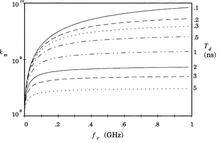
Figure 2.5.2: Maximum gain (given by equation 2.5.9) for different values of loop delay time against the loop filter cut-off frequency
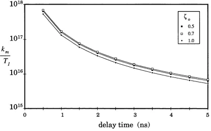
Figure 2.5.3: kJT^ with the loop delay time. Ço=0.707.
Figure 2.5.4: kJT-^ with the loop delay time for a second order loop for several values of relative damping factor.
Figure 2.6.1(a): Spectrum of the phase error signal for a modified first order loop for several values of loop gain. The summed spectrum of the phase noise of the lasers
Si is also shown.
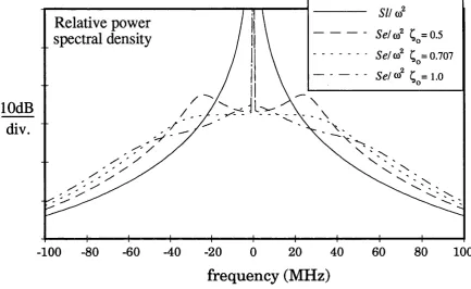
Figure 2.6.1(b): Spectrum of the phase error signal for a second order loop for several values of loop gain. The summed spectrum of the phase noise of the lasers 5/ is also shown. ^^=0.707.
Figure 2.6.2: Spectrum of the phase error signal for a second order loop for several values of relative damping factor. The summed spectrum of the phase noise of the lasers S, is also shown.
Figure 2.6.3: Estimation of the beat signal spectra for several values of loop gain. (a) for a modified first order loop and (b) for a second order loop, ^^=0.707.
Figure 2.6.4: Estimation of the beat signal spectra for several values of relative damping factor for a second order loop.
Figure 2.6.5: Phase error variance for a modified first order loop as function of the loop filter cut-off frequency for several values of loop delay time (maximum loop gain km for each point):
(a) Summed linewidth 5/= 5MHz; (b) Summed linewidth 5/= 2 and lOMHz.
Figure 2.6.6(a): Phase error variance for a modified first order loop as function of the loop delay time for several values of loop filter cut-off frequency (maximum loop gain
k^ for each point).
Figure 2.6.7: Phase error variance as function of Loop delay time 3ns, summed linewidth 5MHz, maximum loop gain is calculated for each point.
Figure 2.6.8: Response of an analogue phase detector.
Figure 2.6.9(a) : for a modified first order loop against the loop delay time for several values of loop filter cut-off frequency (summed linewidth = 5MHz).
Figure 2.6.9(b): for a second order loop against the loop delay time for several values of relative damping factor (summed linewidth = 5MHz).
Figure 2.6.10(a) : Maximum laser summed linewidth against the loop delay time for several values of loop filter cut-off frequency for a modified first order loop (T^^=10years).
Figure 2.6.10(b) : Maximum laser summed linewidth against the loop delay time for a second order loop for several values of relative damping factor =10 years).
Figure 2.6.11(a) : BER^^ against the loop delay time for several values of loop filter cut-off frequency for a modified first order loop when the laser summed linewidth is fixed at 5MHz.
Figure 2.6.11(b) : BER^^ against the loop delay time for a second order loop for several values of relative damping factor, when the summed linewidth is fixed at 5MHz.
Figure 2.6.12(a) : Maximum summed linewidth against the loop delay time for a modified first order loop, for several values of loop cut-off frequency, when BER^^ is given the value of 10'^°.
Figure 2.6.12(b) : Maximum summed linewidth 5/^ against the loop delay time for a second order loop for several values of relative damping factor, when BER^^ is given the value of 10"^®.
Figure 3.2.1: Block diagram of an OPLL using optical fibre. Figure 3.2.2: Block diagram of an OPLL using bulk optics. Figure 3.3.1: Faraday rotation isolator.
Figure 3.3.2: Isolator using quarter-wave plate and polariser.
Figure 3.4.1: Diagram of the wavefronts of two misaligned lasers inciding on a photodetector active region.
Figure 3.4.2: Degradation of the signal power with misalignment. Figure 3.4.3: Procedure for laser alignment.
Figure 3.5.1: Schematic diagram of a DQW-SCH metal-clad ridge waveguide laser. Figure 3.5.2: Output optical power as function of injected current
Figure 3.5.3: Spectrum of a DQW laser.
Figure 3.5.4: Diagram of the set up for the linewidth measurement using self homodyne techniques.
Figure 3.5.5: Linewidth of the DQW-SCH laser against the inverse of output optical power.
Figure 3.5.7: Graph of equation 3.5.5 as function of co Ar.
Figure 3.5.8: Diagram of the experiment used to measure the frequency response of the laser.
Figure 3.5.9: Magnitude (a) and phase (b) of ip for a HLP1400 laser, (proportional to its frequency response).
Figure 3.5.10: Magnitude (a) and phase (b) of a DQW-SCH laser FM response.
Figure 3.5.11: Spectrum of the heterodyne signal when one of the lasers is modulated. Figure 3.5.12: Normalised power spectrum of a frequency modulated signal.
Figure 3.5.13: Magnitude of a DQW-SCH laser FM response using heterodyne method.
Figure 4.2.1: Diagram of the loop configuration.
Figure 4.3.1a: Diagram of the set up for measuring the response of the phase detector. Figure 4.3.1b: Response of the phase detector.
Figure 4.3.2a: Diagram of the set up for measurement of the power levels at the phase detector ports.
Figure 4.3.2b: Plot of the power levels at the phase detector ports.
Figure 4.3.3: Plot of the phase detector gain (KJ against the power R for several values of L.
Figure 4.4.1: Block diagram of a split path amplifier.
Figure 4.4.2a: s plane plot of ideal operation of the low frequency and high frequency amplifiers near the crossover frequency.
Figure 4.4.2b: Frequency response plot of ideal operation of the low frequency and high frequency amplifiers near the crossover frequency.
Figure 4.4.3: Frequency response plot of the operation of the low frequency and high frequency amplifiers near the crossover frequency when they do not present the same cut-off frequency.
Figure 4.4.4: Diagram of the split path amplifier built.
Figure 4.4.5: Frequency response plot of the total split path amplifier. Figure 4.5.1: Laser mounting diagram.
Figure 4.5.2: Equivalent thermal circuit.
Figure 4.5.3: Diagram of the sensor and error signal amplifier circuit (components values in Appendix 6).
Figure 4.5.4: Step function response of the laser mounting. Figure 4.5.5: Basic circuit of a PI filter.
Figure 4.5.6: PI controller used (components values in Appendix 6).
Figure 5.2.1: Block diagram of the basic system assembled in the laboratory for mixing the master and slave laser signals.
Figure 5.3.1: Spectrum of the beat signal of two HLP1400 laser diodes. Figure 5.4.1: Block diagram of the heterodyne OPLL built.
Figure 5.4.2: Spectrum of the beat signal when locking is achieved. Reference -5dBm, 5dB/div, centre frequency 5.1GHz, lOMHz/div. Resolution bandwidth 300kHz.
Figure 5.4.3: Spectrum of the phase error signal in rad^/Hz. Frequency in MHz. Figure 5.4.4: Sequence of beat signal spectrum for several values of loop gain. Reference -30dBm, 5dB/div, centre frequency 6GHz, 5MHz/div.
Resolution bandwidth lOOkHz.
Figure 5.4.5: Spectrum of the beat signal under false locking condition. Reference -35dBm, 5dB/div, centre frequency 6GHz, 20MHz/div. Resolution bandwidth 300kHz.
Figure 5.5.1: Phase error variance against measurement bandwidth.
Figure 5.5.2: Calculated phase error spectrum including the FM response of the slave laser.
Figure 5.5.3: Approximation of the spectrum of the beat signal for several values of loop gain (vertical scale not calibrated).
Figure 5.5.4: Calculated and measured phase error spectrum in rad^/Hz, frequency in MHz.
Figure 6.3.1: Diagram of an OPLL in a planar OEIC structure.
Figure 6.3.2: Diagram of a monolithic multi-quantum well tuned semiconductor laser. Figure 6.3.3: Block diagram of a split path filter for a second order loop.
Figure 6.3.4: Block diagram of a heterodyne second order Optical Phase-Lock Loop using passive filter.
Figure A4.1: Schematic diagram of an external cavity laser. Figure A4.2: Diagram of an anti reflection coating.
Figure A4.3: Relative position of the laser and detector during evaporation.. Figure A4.4: Diagram of the coating thickness control circuit.
Figure A4.5: X-Y recorder plot during evaporation.
Figures A4.6: Characteristic curve after coating for both coated and uncoated facets for two different lasers.
Chapter 1
Introduction
This chapter introduces the optical phase-lock loop (OPLL) and its applications, considers alternative techniques, reviews previous work and describes the contents of the remainder of the thesis.
1.1- The Optical Phase Lock Loop
An optical phase-lock loop (OPLL) is a feedback system which controls an optical source in such a way that the phase of the light from this source follows the phase of an incoming optical signal. This is done by comparing the phase of the input signal to that of the internal source generating an error signal which is used to control the internal source. The internal source which will be controlled will be referred to as the slave laser, while the source of the incoming signal which provides the reference will be called the master laser.
Figure 1.1.1 gives the block diagram of a homodyne OPLL. This system is called homodyne because both master and slave lasers oscillate at the same frequency. Both signals are mixed at the surface of the photodetector, generating a photo-current proportional to the phase difference between the two signals. In the homodyne case the photodetector itself works as phase detector, producing the phase error signal necessary to close the loop. The phase error signal is then treated by the loop filter before being sent to the slave laser which is tuned by this signal in such a way that the phase of its emission is controlled to minimise the error.
master
laser
slave
laser
photo/
phase
detector
loop
filter
C h apter 1- Introduction
Figure 1.1.2 shows a block diagram of a heterodyne OPLL. In this case, master and slave lasers operate at two distinct optical frequencies. The signals from both lasers are mixed on the active area of the photodetector, producing a beat signal at a frequency corresponding to the frequency offset between the two lasers at the photodetector terminals. A phase detector compares the phase of the beat signal to that of an offset generator operating at the same frequency as the beat signal. A phase error signal is then produced at the output of the phase detector and treated by the loop filter. The slave laser is tuned by this signal in such a way that the phase of its emission is controlled to minimise the error.
phase detector
offset
generator
master
laser
slave
laser
photo
detector
loop
filter
Figure 1.1.2: Block diagram o f a heterodyne Optical Phase-Lock Loop.
In heterodyne OPLLs, the output of the slave laser tends to reproduce the whole spectrum of the master laser signal, translating its centre frequency to a new point different from the original one by the frequency of the offset generator. The linewidth of the slave laser is therefore altered by the action of the loop to be the same as the master laser, provided the performance of the loop is adequate. For this reason, heterodyne OPLLs are also known as translation loops [Gardner 79].
Heterodyne OPLLs present several advantages over the homodyne systems. The main advantages are:
-The slave laser frequency can be varied or even swept precisely by varying or sweeping the offset frequency generator.
-AC coupled filters and amplifiers can be used between the photodetector and the phase detector, rejecting DC drifts at the photodetector and improving the loop performance.
C h apter 1- Introduction
1.2- OPLL Applications
In this section, it is seen how the development of the OPLL technology is important for coherent optical communications, providing accurate channel selection, and how OPLLs can be used in these systems. Other more specific applications of OPLLs are also presented.
1.2.1- Coherent Communications
The most common transmission scheme used in optical fibre transmission systems is the intensity modulation (IM) of the optical source with respect to the input electrical signal. In this scheme no attention is paid to the frequency or the phase of the optical carrier, since a photodetector only responds to changes in the power level (the intensity) of an optical signal, and not to its frequency or phase content. Direct detection has been used at the receiving end to reconvert the optical signal into an electrical signal. In this respect a direct detection optical system is analogous to the way a primitive radio detects broadcast signals. This method offers system simplicity and relatively low cost, but suffers from limited sensitivity and does not take full advantage of the tremendous bandwidth capabilities of optical fibres.
Despite the theoretical possibilités, it was only at the end of the 70s that the spectral purity and frequency stability of semiconductor lasers had improved to the point where schemes using heterodyne or homodyne detection of the optical signal began to look feasible. In this technique the light is treated as a carrier medium which can be amplitude, frequency, or phase modulated similarly to the methods used in microwave radio systems.
The two main advantages of coherent optical communication schemes are a nearly ideal receiver sensitivity (up to 20dB improvement over direct detection) [Keiser 91] and a high degree of frequency selectivity. The selectivity of coherent systems is due to the fact that the selection of the channels is made by narrowband electronic filters rather than broad band optical filters.
C h a p ter 1- Introduction
Optical channels using frequency division multiplexing (FDM). This is a direct consequence of the higher selectivity achieved with the microwave filtering at the receiver. The optical channel spacing can now be reduced to frequencies of the order of a few GHz with a corresponding increase in the number of channels.
The advent of fibre amplifiers has diminished the importance of achieving high sensitivity, making the use of coherent techniques not as attractive as in the past for long distance communication links. However, the ability of providing effective demultiplexing for dense FDM systems is still very significant, making coherent systems a good option mainly for local area networks.
Figure 1.2.1 shows the diagram of the frequency response of a nominal 2nm wavelength optical filter, which is equivalent to a frequency bandwidth of 250GHz at the 1550nm region, compared with a 2GHz wide electrical filter. This illustrates that an electrical filter can provide several orders of magnitude more frequency selectivity than an optical one. Thus the channel density of a multichannel coherent system (that is, the number of channels per unit bandwidth) can be 100 times that for direct detection.
2GHz
electrical
. filter
250GHz
optical
filter
frequency
response
frequency
Figure 1.2.1: Diagram o f the frequency response of a nominal 2nm bandwidth optical filter (equivalent to a frequency of250GHz at the 1550nm region) compared with a
2GHz wide electrical filter.
C h apter 1- Introduction
The possibility of actually making such systems depends strongly on the ability to develop truly coherent semiconductor lasers that can be tuned over a significant portion of the 30,000 GHz bandwidth of a single mode optical fibre and the implementation of a proper coding method for inserting data on the optical carrier. Polarisation control of the local oscillator signal to match that of the received signal is also an obstacle to the use of coherent systems. However, several schemes have been proposed to overcome this problem.
Coherent optical detection is thus analogous to superheterodyne detection in modern radios, down converting the information from the optical carrier frequency to a much lower intermediate frequency, where it can be treated electrically. This down conversion is made by mixing the incoming signal with a local oscillator laser operating at a frequency equal to the received central frequency plus or minus the desired intermediate frequency. In the case of homodyne systems, the intermediate frequency is set to be OHz.
A key requirement for the realisation of a coherent lightwave system is the need for an electronically tunable optical source with a high degree of stability and temporal coherency. This is necessary since not only are the optical carriers spaced closely together in the frequency domain but also the modulation is typically encoded onto the frequency or phase of the carrier. The tunable capability of the laser allows the generation of both the optical transmitter channels and the local oscillators at the heterodyne receivers.
One technique to generate closely spaced optical channels is based on an optical frequency translation loop. This can take the form of either an optical phase-locked loop or an optical frequency-locked loop. The translation loop generates the channels by frequency off-setting the current controlled oscillator laser, within the loop, from a stable reference source, ideally to generate a large number of channels. This reference could be one frequency from an optical comb of frequencies.
1.2.2- Carrier generation in dense FDM systems
C h apter 1 - Introduction
Figure 1.2.2 shows a block diagram of a carrier generator system using heterodyne OPLLs. A stable narrow linewidth master laser is used as reference for a chain of OPLL sub-systems. As the OPLL makes the slave laser reproduce the spectrum of the master laser at an offset frequency, the carriers are synthesised by using a sample of the slave laser signal from each OPLL block as master signal for the following one. The spacing between the carriers can be adjusted individually by tuning each offset generator, while the whole comb of carriers can be tuned by tuning the master laser optical frequency. master laser stable reference photo detector phase detector — slave laser loop filter offset generator 1st carrier photo detector phase detector
— ®
- ©
slave laser V loop filter offset generator 2nd carrier1
to the next OPLLFigure 12.2: Block diagram of a carrier generator system using OPLLs.
1.2.3- Phase demodulator
If the phase of the master laser is modulated, the OPLL will see this modulation as phase error and it will try to modulate the slave laser equally in an attempt to cancel this "error". A signal proportional to the modulating signal becomes available at the phase detector output, as shown in Figure 1.2.3. Frequency demodulation can be achieved in the same way, as the frequency is given by the time derivative of the phase.
C h apter 1- Introduction
master
' coupler
photo laser
f
1
1 TTT detectordata in
transm itter
phase \ detector .
slave laser
\
loop filter
offset I generator
data p u t I
receiver
Figure 1.2.3: Block diagram of a optical phase modulation (PM) system using an OPLL as phase demodulator.
1.2.4- Local Area Networks (LANs)
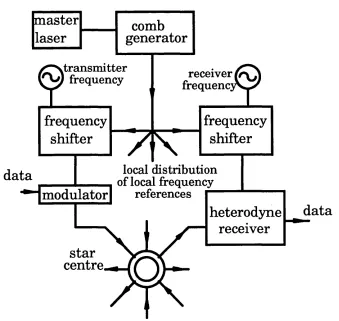
A good example of the application of OPLLs was the European program ESPRIT 2054 Project UCOL (Ultra-wideband Coherent Optical LAN) [Fioretti 89] [Fernando 90]. Figure 1.2.4 shows a diagram of this system.
master
comb
laser
generator
✓^^transmitter frequencyfrequency
shifter
receiverfrequencj^Y^
frequency
shifter
data
“^ m o d u la to r
local distribution of local frequency
references
heterodyne
receiver
c l n t r e ^ Q
data
C h a p te r 1- In trodu ction
A comb of optical signals is distributed to every station as frequency references to which frequency shifters would be locked^ to provide both an optical carrier for transmitting and a local oscillator for the coherent reception. Again heterodyne OPLLs could be used as frequency shifters.
This kind of system could be used in a metropolitan area network (MAN) to integrate data voice and video transmission. However, such a system would only be feasible if stable and reliable OPLLs were available. Optoelectronic integrated circuit (OEIC) techniques may provide this in the future, also helping to bring the costs down.
1.2.5- Phased array antennas
The amplitude and the phase of the current at each element of the array determine the pattern of the radiated beam, while the number of elements sets the resolution of the antenna. A beam forming network is necessary to feed each element individually with the proper amplitude and phase to achieve the required pattern. However, when the number of elements is high, it becomes difficult to construct these networks using conventional waveguides or coaxial cables due to their size, weight, loss and narrow bandwidth. The use of optical fibres comes as a solution to these problems, being small, flexible, lightweight and practically immune to electromagnetic interference. Also, they have negligible losses, good phase accuracy and very large bandwidths. The optical fibre distribution network can not only provide the beam control, but also the distribution and transmission of the communication signal and the distribution of the phase and frequency reference.
Optical beam forming networks (OBFNs) can be produced by direct detection methods [Benjamin 90] or by coherent methods [Ghese 91]. When direct detection techniques are used, the lasers employed need to have a modulation bandwidth corresponding to the microwave frequency of the communication signal carrier, which is very difficult to obtain especially when high phase accuracy is required. However, it is possible to obtain a better carrier to noise performance with coherent schemes than with direct detection schemes, resulting in a better power budget which allows for more arrays or fewer laser transmitter modules. Furthermore, the generated microwave frequency at the antenna can easily be tuned by simply tuning one of the two lasers employed. Coherent techniques also give more possibilities for optical control and optical processing [Gliese 91].
C h a p ter 1- Introduction
antenna transmitting frequency. The data to be transmitted modulates the master laser after a sample is taken for the phase locking of the salve laser. The beat signal is recreated at each element and amplified before being transmitted. A specific delay time is introduced using optical fibre delay lines for each element, providing the phase shift required for the individual element.
m o A t q r d a ta in
master laser
photo detector
fibre network At
detector amplifier antenna
\ r /
At
C H > -(
1
offset
....
n
g ) ^ generator
phase detector
C H > -(
Figure 1.2.5: Block diagram of an OBFN using coherent techniques.
1.2.6- Optical sweep generator and optical measurements
It is possible to see from the block diagram of the heterodyne OPLL (Figure 1.1.2) that, if the offset generator is swept in frequency, this sweep will be transfered to the optical frequency of the slave laser in relation to the master laser. An optical sweep generator can then be built using an heterodyne OPLL, with applications in spectroscopy and optical measurements.
1.3- Comparison with other technologies
1.3.1- Optical Frequency Lock Loop
C h apter 1- Introduction
filter arranges the error signal which tunes the slave laser in order to compensate for any fluctuation of the offset frequency.
master
photo
laser
detector
mixer
slave
loop
1
laser
filter
frequency
offset
generator
Figure 1.3.1: Block diagram o f an optical frequency locked loop.
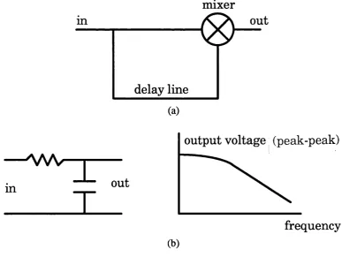
The frequency discriminator is basically a device whose frequency response presents a slope which can be approximated as linear. This can be achieved by a combination of a balanced mixer and a delay line in a kind of interferometer, as shown in Figure 1.3.2a. Alternatively, a low pass filter can be used, as in Figure 1.3.2b.
mixer
m
out
delay line
(a)
— ^ V W
in
T
I
out
output voltage (peak-peak)
frequency
(b)
C h a p te r 1- In trodu ction
In OFLLs, the centre frequency of the slave laser is controlled and kept stable in relation to the centre frequency of the master laser. Fluctuations of the central frequency of semiconductor lasers are usually slow (below lOOkHz) due to the Iff
noise component of the FM noise spectrum [Fernando 91]. Therefore, narrow band loops can be used and the loop delay time is not an important factor.
The advantage of using a heterodyne OPLL instead of an OFLL is that not only the centre frequency of the beat signal is fedback by the loop, but also the instantaneous phase. The whole spectrum of the slave laser is altered by the action of the loop, making the slave laser reproduce the line shape of the master laser at a new centre frequency. This feature becomes particularly important when several narrow linewidths signals are required at different frequencies. In this case, only one narrow linewidth laser is required, while the others have their linewidths narrowed when locked to this reference.
1.3.2- Injection Locking
Phase lock is also possible though injecting the signal from the master laser into the active region of the slave laser waveguide [Kobayashi 80] [Lidoyne 91]. Figure 1.3.3 gives a diagram of an injection locking experiment.
mirror
master
laser
lens
slave
optical isolator
laser
Figure 1.3.3: Diagram of an injection locking experiment.
C h apter 1 - Introduction
at different frequencies by modulating the master laser and locking the slave laser to one of the sidebands generated by the modulation of the master laser signal. The main disadvantage of this method is that the frequency offset is limited by the frequency response of the laser, while for the OPLL it is limited by the response of the photodetector, the phase detector and the offset generator, which are already well developed components and available for high frequencies.
Figure 1.3.4 shows a diagram of a coherent receiver using injection locking. A sample of the incoming signal is taken though an optical isolator to lock the slave laser to its frequency and phase. The output of the slave laser is then combined coherently to the incoming signal, producing a beat signal at the photodetector terminals. One disadvantage of this kind of system is that a part of the incoming optical signal has to be used to injection lock the slave laser before detection takes place, reducing sensitivity.
m aster
laser lens photo
detector
optical isolator slave
laser
Figure 1.3.4: Diagram of a coherent receiver using injection locking.
1.3.3- Other technologies
Direct modulation can be used for optical carrier generation by using mode-lock techniques to generate a comb of optical frequencies. However, it has the disadvantage of having the frequency offset between carriers fixed to the laser mode space of the laser.
Integrated-optic frequency translators can be used to introduce a frequency shift to an optical carrier. This can be done by using single side band (SSB) modulation techniques [Izutsu 81] [Culshaw 81], in which the side band becomes the new offset optical signal. Other devices are based on an electrooptic effect associated with a propagating microwave field to offset an incoming optical carrier by the frequency of the microwave signal used [Désormière 90].
C h a p ter 1- Introduction
1.4- OPLL critical parameters
Because most of the phase noise spectrum of the beat signal is used by the control loop, the loop bandwidth has to be wide enough to cover the main frequency range of this noise. The principal critical parameters in the OPLL design are:
- Laser linewidth: The main source of noise is the phase noise originated in the lasers used in the system. The extension of the spectrum of this noise is given by the laser linewidth, considering Lorezian lineshape.
- Loop bandwidth: When wide linewidth lasers are used, a wide bandwidth loop is required to track the phase noise.
- Loop delay time: The loop propagation delay time limits the bandwidth of the system and it is a particularly important factor when wide linewidth lasers and wide bandwidth loop filters are used.
These factors and the relationship between them will be studied quantitatively in Chapter 2 of the thesis.
The implementation of OPLLs in opto electronic integrated circuit OEIC form will only be possible in the future if semiconductor lasers are used. As these lasers normally possess wide linewidth, wide bandwidth loops need to be used. The effect of the loop delay time is expected to be minimised by its decrease due to the reduction in size brought about by integration.
1.5- Historical Background
1.5.1- Experimental work
The use of phase-lock techniques at optical frequencies has been limited in the past by a series of technological problems. The most important factor has been the unavailability of suitable optical sources. Problems of wideband phase noise, frequency instability and tunablity were the main obstacles to the use of laser sources as slave lasers in OPLLs. In this introduction a brief review of the OPLL experiments reported is presented.
C h apter 1- Introduction
mirror. The use of semiconductor laser diodes would make the tuning system simpler and faster, as they could be directly tuned by current. Nevertheless, wideband phase noise prevented their use. The first experiment using semiconductor lasers [Steele 83] applied weakly coupled external cavities to the laser diodes in order to narrow then- line widths. In this heterodyne system, locking was obtained only for short periods due to acoustic frequency jitter and thermal drift affecting the external cavities. The same kind of experiment was done without intentional optical feedback [Richards 85]. However, the loop was not completely stable due to the large amount of phase noise and operation was only obtained over a short period of time.
Homodyne OPLLs were reported later using piezoelectric tuned HeNe lasers [Malyon 84] and LiNbO^ modulator tuned external cavity semiconductor lasers locked to a HeNe laser [Malyon 86]. Heterodyne systems with an offset frequency of 5MHz using HeNe lasers were also achieved [Hall 87]. Solid state Nd:YAG ring lasers operating at 1320nm pumped by laser diodes were used in a homodyne OPLL presenting a natural frequency/^=36kHz [Kazovsky 89 and 90] and/„=10kHz [Schdpflin 90]. The same technique was also used for heterodyne loops [Williams 89], with/^=36kHz and offset frequency of 4GHz [Atlas 90], and/„=50-100kHz and offset frequency of 12GHz [Wale 91].
Improved external cavity semiconductor lasers were used in a heterodyne OPLL at a 250MHz offset, presenting a natural frequency/„ of the order of 300kHz [Harrison 89] and in a homodyne system with/„ of about lOOkHz [Kahn 89]. External cavity three electrode DFB lasers were also used in a homodyne system with 22ns loop delay time and /„=605kHz [Noiiamtsu 90]. Another way of narrowing the linewidth of semiconductor lasers was to employ optical feedback from external high finesse resonators. This technique was used in heterodyne OPLLs with 25MHz offset frequency and/„=263kHz [Shin 90] and with 20ns loop delay [Telle 90].
C h a p ter 1- Introduction
In Chapter 5, the first heterodyne OPLL experiment using semiconductor lasers without external cavities or other linewidth narrowing methods is described. This is also the heterodyne OPLL with the widest natural frequency (20MHz) and lowest delay time (3ns) [Ramos 92].
1.5.2- Theoretical work
As previous experimental work was done using very narrow linewidth lasers, it was not clear what the maximum value of phase noise was which would still allow the loop to lock. This limit depends strongly on the value of the loop bandwidth, as the phase noise suppression effect within the loop bandwidth is affected. Another important factor is the propagation delay time of the loop, which has great influence on the loop performance and stability, as it also limits the loop bandwidth. There was then the need for developing a theoretical study in order to understand better the influence of the adverse noise characteristics of lasers on OPLL systems.
The first step was to identify the main sources of noise in the system and relate the phase noise to a parameter of quality of locking, such as the phase error variance [Armor 79]. Following this analysis, attempts were made to optimise the design of OPLLs [Hodgkinson 85]. The same approach for optimisation was used and linewidth limits were set for a given bit error rate (BER) [Kazovsky 86]. The influence of the loop propagation delay time was then considered [Grant 87]. A modified first order loop was shown to be more suitable for OPLLs with large phase noise [Steele 88].
C h apter 1- Introduction
between cycle slips is also introduced, together with a full discussion on the loop performance.
1.6- Structure of the Thesis
The first objective of this thesis is to demonstrate that commercial OPLLs can be feasible in the future by understanding their limitations, modelling the system and setting design guide lines. The second objective is to build an OPLL in the laboratory.
Chapter 2 presents the theoretical analysis of the OPLL. The block diagram and transfer functions of both homodyne and heterodyne OPLLs are presented and the main sources of noise are identified. Then discussions on the loop filter design and the loop stability are introduced for a non zero loop propagation delay time. Methods of evaluating the loop performance are shown and a cycle slip criterion is established to determine loop parameters during design.
Chapter 3 concentrates on the design of the optical section of the OPLL experiment. Some comments are made on how the optical mixing is carried out, followed by a discussion on optical isolation and an evaluation of the amount of optical misalignment tolerable in order to obtain effective optical mixing. The main characteristics of the double quantum well lasers (DQW) used in the final experiment are presented. As part of this characterisation, the FM response of a DQW laser is measured
Chapter 4 discusses the design of the electrical part of the OPLL, starting by giving an overview of the loop circuit, followed by a description of the phase detector. A design of the phase error amplifier (which is the loop filter) is presented, showing how a split path technique is used to reduce delay time effects. Finally, the temperature control system design is described.
Chapter 5 shows the final OPLL experiment, using the ideas and techniques detailed in the previous chapters. The measured performance is presented, followed by the parameters calculated from the measurements and a comparison to the theoretical predictions. This experiment demonstrates for the first time a stable heterodyne OPLL using semiconductor lasers without external cavities or any other linewidth narrowing process.
C h a p ter 1- Introduction
References:
Armor, J.B., Robinson, S., "Phase-lock control considerations for coherently combined lasers", Appl. Opt., 1979,18(18), pp. 3165-3175.
Atlas, D.A., Kazovsky, L.G., "2 Gbit/s PSK heterodyne communication system using optical phase-locked loop". Electronics Letters, 1990, 26(14), pp. 1030-1032.
Benjamin, R., Zaglanikis, C. D. and Seeds, J. A., "Optical Beam Former for Phased Arrays with Independent Control of Radiated Frequency and Phase", Electronics Letters, vol. 26, n. 22, 1990, pp. 1853-1855.
Culshaw, B. and Wilson, M. G. F., "Integrated Optic Frequency Shifter Modulator", Electronics Letters, vol. 17, 1981, pp. 135-136.
Désormière, B., Maerfeld, C. and Desbois, J., " An Integrated Optic Frequency Translator for Microwave Lightwave Systems", Journal of Lightwave Technology, vol. 8, n. 4, April 1990, pp. 506-513.
Fernando, P. N., Fake, M. and Seeds, A. J., "A Novel Approach to Optical Frequency Synthesis in Coherent Lightwave Systems", Proceedings of SPIE, O/E Fibres, vol.
1372, 1990, pp. 152-163.
Fernando, P. N., Ramos, R. T. and Seeds, A. J., "Optical Carrier Synthesis in Coherent Lightwave Systems", lEE Colloquium on Sources for Coherent Optical Communication, digest n. 1991/013, London, 18 January 1991, pp. 12/1-12/7.
Fioretti, A., Neri, E., Forcesi, S., Gree, A., E., Fernando, P. N., Labrujere, A. C., Koning, O. J., BekooiJ, J. P., Veith, G., Shmuck, H., "Technology Aspects of a Coherent Optical M.A.N.", Proceedings of SPIE, vol. 1175,1989, pp. 182-195.
Gardner, F.M.: Phaselock Techniques, (Wiley, New York, 2nd Ed., 1979).
C h apter 1- Introduction
Grant, M.A., Michie, W.C., Fletcher, M.J.: "The performance of optical phase locked loops in the presence of nonnegligible loop propagation delay", J. Lightwave Tech., 1987, LT5, pp. 592-597.
Harrison, J. and Mooradian, A., "Linwidth and Offset Frequency Locking of External Cavity GaAlAs Lasers", Journal of Quantum Electronics, vol. QE-25, n. 6, June, 1989, pp. 1152-1155.
Hall, J. L., Sheng, M. L., Kramer, G., "Principles of Phase-Locking: Application to Internal Mirror He-Ne Lasers Phase-Locked via Fast Control of the Discharge Current", Journal of Quantum Electronics, vol. QE-23, n. 4, April, 1987, pp.427-437.
Hodgkinson, T.G.: "Phase locked loop analysis for pilot carrier coherent optical receivers". Electronics Letters, 1985, 21, pp. 1202-1203.
Izutsu, M., Shikama, S. and Sueta, T., "Integrated Optical SSB Modulator/Frequency Shifter", IEEE Journal of Quantum Electronics, vol. QE-17, n. 11, November, 1981, pp. 2225-2227.
Kahn, J.M., Kasper, B. L. and Pollock, K. J., "Optical Phaselock Receiver with Multigigahertz Signal Bandwidth", Elect. Lett., 1989, vol. 25, n. 10, pp. 626-628.
Kahn, J.M., "1 Gbit/s PSK homodyne transmission system using phase-locked semiconductor lasers", Photonics Tech. Lett., 1989, vol. 1(10), pp.340-342.
Kazovsky, L. G., "Performance Analysis and Laser Linewidth Requhements for Optical PSK Heterodyne Communications Systems", J. Lightwave Tech., vol. LT-4, n. 4, April 1986, pp. 415-425.
Kazovsky, L.G., Atlas, D.A., "A 1320 nm experimental optical phase-locked loop", Photonics Tech. Lett., 1989, vol. 1(11), pp.395-397.
Kazovsky, L.G., Atlas, D.A., "A 1320 nm experimental optical phase-locked loop: performance investigation and PSK homodyne experiments at 140 Mb/s and 2 Gb/s", J. of Lightwave Tech, 1990, 8(9), pp. 1414-1425.
C h apter 1- Introduction
Kobayashi, S. and Kimmura, T., "Injection Locking Characteristics of an AlGaAs Semiconductor Laser", IEEE Journal of Quantum Electronics, vol. QE-16, n. 9, September 1980, pp. 915-917.
Kourogi, M., Shin, C.H., Ohtsu, M., "A 134MHz bandwidth homodyne optical phase- locked-loop of semiconductor laser diodes", Photonics Tech. Lett., 1991, vol. 3(3), pp.270-272.
Leeb, W.R., Philip, H.K., Scholtz, A.L., Bonek, E.: "Frequency synchronization and phase locking of COj lasers", Appl. Phys. Lett.,1982, vol. 41(7), pp.592-594.
Lidoyne, O., "Bruit de Phase et Modulation d'un Laser a Semi-Conduteur Synchronise; Applications aux Telecommunications", Doctor degree thesis. Ecole Nationale Supérieure des Télécommunications, Paris, France, 1991.
Malyon, D.J., "Digital fibre transmission using optical homodyne detection". Elect. Lett., 1984, vol. 20(7), pp.281-283.
Malyon, D.J., Smith, D.W., Wyatt, R.: "Semiconductor laser homodyne optical phase locked loop". Elect. Lett, 1986, 22(8), pp.421-422.
Norimatsu, S., Iwashita, K., Noguchi, K., "10 Gbit/s optical PSK homodyne transmission experiments using external cavity DFB LDs", Elect. Lett., 1990, vol. 26(10), pp.648-649.
Norimatsu, S., Iwashita, K., Sato, K., "PSK optical homodyne transmission detection using external cavity lasers diodes in Costas loop", Photonics Tech. Lett., 1990, 2(5), pp.374-376.
Ramos, R.T., Seeds, A.J., "Delay, linewidth and bandwidth limitations in optical phase-locked loop design". Elect. Lett., 1990, vol. 26(6), pp.389-391.
Ramos, R.T., Seeds, A.J., "Fast Heterodyne Optical Phase-Lock Loop Using Double Quantum Well Laser Diodes", Elect. Lett., 1992, vol. 28, n.l, pp.82-83.
C h apter 1- Introduction
Shin, C.H., Ohtsu, M., "Optical Phase-Locking Expeirments by Confocal Fabry-Perot Cavity Coupled Semiconductor Lasers", Third Optoelectronics Conference (OEC90) Technical Digest, July, 1990, Makuhari Messe.
Scholtz, A.L., Leeb, W.R., Flatscher, R. and Philip, H.K., "Realization of a lO-p-m Homodyne Receiver", Journal of Lightwave Technology, vol. LT-5, n. 4 April, 1987, pp. 625-632.
Schopflin, A., Kugelmeier, S., Gottwald, E., Ffelicio, D., Fischer, G., "PSK optical homodyne system with nonlinear phase-locked loop". Elect. Lett., 1990, 26(6), pp.395-396.
Steele, R.C., "Optical phase locked loop using semiconductor laser diodes", Elect. Lett., 1983, vol. 19, pp.69-71.
Steele, R.C., Creaner, M.J., Walker, G.R., Walker, N.G.: "Optical PSK transmission experiment at 565Mbit/s incorporating an endless polarization control system". Proceedings of SPIE Components for Fiber Optics Applications and Coherent Lightwave Communications, Boston, 1988, vol. 988, pp. 302-309.
Telle, H.R., Li, H., "Phase-Locking of Laser Diodes", Electronics Letters, 1990, vol. 26, n. 13, pp.858-859.
Wagner, S. S. and Kobrinski, "WDM Applications in Broadband Telecommunication Networks", IEEE Communications, March 1989, pp. 22-30.
Wale, M.J., Holliday, M.G., "Microwave signal generation using optical phase locked loops". Workshop A Proceedings, European Microwave Conference, Stuttgart, 1991, pp. 77-82.
Chapter 2
Optical Phase-Lock Loop Theory
2.1- Introduction
As the ability to obtain stable single mode laser radiation developed during the early 1980s, the translation of phase lock techniques in use at microwave frequencies to optical frequencies was slowly made possible. Some OPLL experiments started to be reported, all using very narrow linewidth lasers (order of lOOkHz or less). This was achieved using gas lasers like CO2 and HeNe, solid state lasers like YAG lasers and semiconductor lasers using external cavity optical feedback or electrical feedback. A full review of the OPLL experiments and theoretical work was presented in Chapter 1.
In this Chapter we extend previous analysis [Grant 87] [Steele 88] to include finite loop propagation delay together with photodetector shot noise, and derive design criteria for OPLLs as a function of the loop parameters. First, the block diagram and transfer functions of both homodyne and heterodyne OPLLs are presented and the main sources of noise are identified. Then discussions on the loop filter design and the loop stability are introduced for a non zero loop propagation delay time. Methods of evaluating the loop performance are shown and a cycle slipping criterion is established to determine loop parameters during design. Finally, the conclusions are summarised.
2.2- Block Diagram and Transfer Functions
2.2.1- Homodyne case:
The block diagram of a basic Phase-Locked Loop (PLL) is shown in Figure 2.2.1. The master signal y j t ) and the slave oscillator signal yj(t) are given by:
y ^ n i t ) = A sin(co^/ + 4)^(0) 2.2.1
C h apter 2: O ptica l P h a se -L o c k L o o p Theory
phase
detector
loop
filter
slave
oscillator
Figure 2.2.1: Block diagram o f a general phase-lock loop.
Where A and B are the amplitudes, co^ and O)^ are the angular frequencies and and (|)/rj are the phases of master and slave oscillator signals respectively.
Considering first that the master and slave signals have the same frequency, the signal after the phase detector Uj(t), for a sinusoidal phase detector, would be:
Uj(t) = ka
sin[(|)„(0-
2.2.3Where k^ is the phase detector gain. \îf(t) is the impulse response of the loop filter and
kg represents the gain of this filter, U2(t) will be given by the convolution of Uj(t) with f(t) as follow:
« 2 (0 = 4 2.2.4
Using a tunable slave oscillator which has its output frequency dependent on the amplitude of the input signal, the output phase ^Jt) will be:
_
d t — ^2 (^) 2.2.5
Where k^ is the slave oscillator gain. Using equations (2.2.4) and (2.2.5):
C h apter 2: O ptica l P h a se -L o c k L o o p Theory
Where k is the total gain, given by:
k — kg kg 2.2.7
For small amounts of phase error (phase error variance lower than 7i/2rad^), it is possible to use a linearised model of the phase detector:
= 2.2.8
a t
Using Laplace transformation in order to pass to the frequency domain:
j 4)j(s) = ^ :[ 3 ) „ (î) - O j(j) ] F (j) 2.2.9
The loop transfer function is defined as:
O m W S + K F { S )
For the phase error given by:
2.2.11
One can write:
= ^ = = ^ 2.2.12
< D „ W s + K F { s )
Figure 2.2.2 shows the block diagram of a homodyne optical phase-locked loop. The master laser and the slave laser operate at the same optical frequency while the photodetector works as a phase detector. In this case the phase detector gain has the same value of the photodetector gain kp , given by:
kp = 2 R ^ P ^ P, 2.2.13
C h apter 2: O ptica l P h a se -L o c k L o o p Theory
coupler
slave
laser
master
laser
photo
detector
loop
filter
Figure 2.2.2: Homodyne optical phase-lock loop.
2.2.2- Heterodyne case:
Figure 2.2.3 shows the block diagram of a heterodyne OPLL. In this case, the optical frequencies of master and slave lasers are separated by a reference value co^.
phase
master
photo
U^(t) ^laser
'
~ r mdetector
\offset
generator
u^it)
Figure 2.2.3: Heterodyne optical phase-lock loop.
The photodetector produces a signal centred on co^, u^it):
C h apter 2: O p tica l P h a s e -L o c k L o o p Theory
U4 ( 0 = C COS[(Ù^t + (|)^ (0 1 2 ,2.15
Uj ( t ) = kp sin [(t)^ (0- * , ( 0 - (^rO)] 2 .2.16
Where is a constant of the phase detector. In this case, the total gain k must include
k^ and kp as follows:
k = k d k p k g k g 2.2.17
The new phase error is given by:
0 / j ) = W 2.2.18
2.3- Sources of Noise
Looking at the block diagram of a heterodyne OPLL, Figure 2.2.3, it is possible to identify the major sources of noise:
-phase noise of the master laser signal. -phase noise of the slave laser signal. -photodetector shot noise.
-phase noise of the offset reference signal. -master and slave laser amplitude noise.
-other noise generated in some of the OPLL building blocks such as frequency mixers, wideband amplifiers, the phase detector and dc bias circuits.
In the analyses shown in this chapter, only the main sources of noise will be taken into account as they restrict the design of the system. The use of balanced receivers can reduce the effect of the intensity noise [Patzak 89], which is normally small (relative intensity noise between -140 and -150dB/Hz). For this reason and the fact that it can not be compensated by the action of OPLL, the intensity noise will not be considered in the analysis. It is possible to estimate the contribution of each of these noise sources towards the phase error 0^ by using the loop transfer function as follows [Ohtsu 92]:
C h apter 2: O p tica l P h a s e -L o c k L o o p Theory
Where is the master phase fluctuation, is the slave laser phase fluctuation and N^.
offset reference oscillator phase fluctuation. is the phase translated fluctuation due to the detector shot noise, which is given by multiplying the electrical shot noise by the phase detector constant. Figure 2.3.1 shows a block diagram of the linearised model of the heterodyne OPLL indicating the main sources of noise.
master laser
phase noise
phase translated
shot noise
master
laser
offset generator
phase noise
slave laser _
phase noise
loop
filter
slave
laser
1/s
kF( s )Figure 2.3.1: Block diagram of the OPLL indicating the main sources o f noise.
The behaviour of the main sources of noise will be given by the double sided spectra of the master laser phase noise (5 J , slave laser phase noise (S) and detector shot noise % .).
From now on, the phase noise of the offset frequency generator will not be taken into account since it is usually much smaller than the first three noise sources (the linewidth of a reference signal generator operating at a few GHz would not be expected to exceed lOOHz, while the laser linewidths are of the order of MHz). Other minor sources of noise are also neglected.
2.3.1- Laser Phase Noise
C h apter 2: O ptica l P h a se -L o c k L o o p Theory
Semiconductor laser FM noise usually consists of several components [Yamamoto 83] [Ohtsu 92]. The first main component is the frequency fluctuation originating from spontaneous emission resulting in white FM noise. The line a in Figure 2.3.2 represents the spectral density of such noise.
10
®o_
.4 .7
.2 ,3 .5 .8 .9 ,10
frequency (Hz)
Figure 2.3.2: Schematic representation o f the spectral density o f a single mode semiconductor laser FM noise (e). The different components are due to:
a- spontaneous emission resulting in white FM noise, b- fluctuation o f the carrier density,
c- slow component due to self heating, d- flicker noise or 1 If noise.