Sharif University of Technology
Scientia IranicaTransactions D: Computer Science & Engineering and Electrical Engineering www.scientiairanica.com
Low cost circuit-level soft error mitigation techniques
for combinational logic
R. Rajaei
a;, M. Tabandeh
aand M. Fazeli
ba. Department of Electrical Engineering, Sharif University of Technology, Tehran, Iran.
b. Department of Computer Engineering, Iran University of Science and Technology, Tehran, Iran. Received 28 October 2014; received in revised form 21 June 2015; accepted 22 August 2015
KEYWORDS Soft Error (SE); Single Event Transient (SET);
Multiple Event Transient (MET); Single Event Upset (SEU);
Single Event Multiple Upset (SEMU); Single Event Multiple Transient (SEMT).
Abstract. Following technology scaling trend, CMOS circuits are facing more reliability challenges such as soft errors caused by radiation. Soft error protection imposes some design overheads in power consumption, area, and performance. In this article, we propose a low cost and highly eective circuit to lter out the eect of particle strikes in combinational logic. This circuit will result in decreasing Soft Error Propagation Probability (SEPP) in combinational logic. In addition, we propose a novel transistor sizing technique that reduces cost-eciently Soft Error Occurrence Rate (SEOR) in the combinational logic. This technique generally results in lower design overhead as compared with previous similar techniques. In the simulations run on dierent ISCAS'89 circuit benchmarks, combining the proposed techniques, we achieved up to 70% SER reduction in the overall soft error rate of the circuits for a certain allowed overhead budget.
© 2015 Sharif University of Technology. All rights reserved.
1. Introduction
Radiation induced Soft Errors (SEs) are of the main challenges in design of Nano-scale VLSI circuits. Al-though technology scaling oers better performance, smaller area, and lower power consumption in digital circuits, it increases the sensitivity of circuits to ener-getic particles resulting in lower reliability [1]. When an energetic particle strikes an o-state drain of a CMOS transistor, it would deposit its energy in the struck region. The deposited energy would cause a transient voltage glitch in the aected node. This voltage glitch is referred to as Single Event Transient (SET). If the aected node belongs to a memory element such as a latch or a ip-op, the transient voltage may change the stored value. This phenomenon is called Single
*. Corresponding author. Tel.: +98 21 66384366; E-mail addresses: [email protected] (R. Rajaei); [email protected] (M. Tabandeh); m [email protected] (M. Fazeli)
Event Upset (SEU). Generally, the eect of particle strike can be classied as SEU and SET. SEU and SET refer to the eect of particle strike in sequential and combinational logic [1-3].
With the scaling trend of technology sizes toward nanometer era, the probability that a particle strike af-fects more than one node and causes multiple transient voltage glitches in adjacent nodes is rapidly increasing. It means that today, VLSI circuits should deal with Single Event Multiple Eects (SEME). Single Event Multiple Upsets (SEMU) and Single Event Multiple Transients (SEMT) are today's reliability challenges of Nano-scale circuits in sequential and combinational parts. Soft error mitigation techniques in digital circuits incur area, performance, and power penal-ties [3,4]. In design of reliable digital circuits, it is important to make a reasonable trade-o between the reliability improvement and its related area, power, and performance cost. Previously proposed techniques for SE protection mainly do not consider the eect of SEMEs. Moreover, design overhead resulted from the
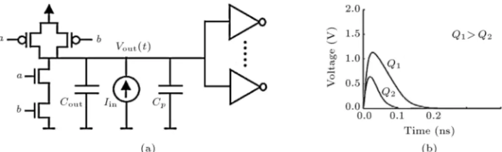
Figure 1. SE injection: a) A two inputs NAND gate and an SE injection to its output node; and b) transient voltage pulse at the strike region.
employed SE protection techniques considerably aects the design improvements gained by the new technology scales [2-5].
In this article, we try to improve the combina-tional logic reliability meeting the design constraints such as area and performance. In other words, the main goal is obtaining required reliability while imposing lower overhead comparing with previous techniques. To achieve this, at the rst step, we should identify the gates/paths of the combinational part, which have more sensitivity to soft errors in order to selectively apply our proposed techniques for soft error protection. For this reason, we use the method proposed in [5] for accurate and also fast estimation of Soft Er-ror Propagation Probability (SEPP) in combinational logic. Using this method, we identify more susceptive parts (i.e. gates and paths) of the circuit that have more impact on total circuit unreliability. Then, we employ our proposed techniques/algorithms to protect the identied parts in order to improve the circuit reliability imposing a reasonable overhead.
Our main contributions regarding Soft Error (SE) protection in combinational logic, which will be pre-sented in the following sections of this article, include:
1. Proposing a new gate resizing method that consid-ers gate inputs and their associated probabilities in order to have an eective and also cost-ecient SE protection. We refer to it as Cost-Aware Transistor Sizing method or simply CATS;
2. Proposing an eective, Low Delay and also Tunable (LDT) SET lter circuit for eliminating the SET pulses at the last possible time before reaching sequential logic or Primary Outputs (POs);
3. Oering an algorithm that, considering timing and area constraints, tries to eciently employ the pro-posed CATS and LDT SET lter circuit together in order to improve soft error robustness while having a reasonable overhead.
At rst, we proposed Algorithm-A and Algorithm-B to investigate the eects of the CATS rule and LTD SET lter circuit on soft error tolerance, individually.
Then we concluded Algorithm-C that is composed of the prior algorithms.
2. Backgrounds and preliminaries
In this section, we review some preliminary knowledge regarding SE modeling, SER estimation, and SE pro-tection in combinational logic.
2.1. Soft error modeling and soft error rate estimation
In order to model the eect of a particle strike in CMOS circuits, we have employed a double-exponential current model to mimic the behavior of a radiation-induced fault (Figure 1(a) and (b)). Using this model, we inject a fault into the desired fault site [1,2,5,6].
Iinj= Q a b
e at e bt ; (1)
where, Q denotes the (positive/negative) deposited charge, a and b are the collection time constants
of the junction and the ion-track establishment time, respectively. These time-constant parameters are de-pendent on various process related factors [7].
As mentioned above, in order to have a cost-ecient reliable design, Soft Error Rate (SER) es-timation is essential. Identifying the gates of the circuits with higher impact in overall circuit reliability, we could consider them as candidates for SE pro-tection. As SE protection would impose signicant overhead in performance, area, and power, selective protecting in CMOS circuits is a widely used approach in similar cases by researchers. An accurate and also fast estimation of SER could help us to identify the gates or paths of the circuit that have higher impact on circuit reliability and also evaluate eciency of the SE protection techniques. The SER of the circuit can be assumed as product of two metrics: SE Occurrence Rate (SEOR) and probability of SE propagation (SEPP). In the remaining of this article, we would consider the total SER of a circuit as:
SERtotal=
all gates of the circuitX k
(SEORGk SEPPGk):
In [3,5,8-10], various SER estimation techniques (mostly SEPP estimation techniques) have been pro-posed. Among all, the technique presented in [5] is a fast and also accurate method for SEPP estimation. This considers all three masking factors of the circuit. Moreover, it considers SEMTs in its computations. In [5], it has been reported that this technique has a high level of accuracy, while it has a signicant speedup factor (of up to 10000X) in comparison with simulation based fault injection.
The employed SER estimation technique (pro-posed in [5]) is based on a four-value probability system and a static timing analysis method that propagates all faulty pulses produced as a result of an SEMT event from originated fault site to reachable FFs/POs. At the rst step, this technique nds fault sites. A heuristic technique for identifying the adjacent gates for a given gate is proposed in this article. Based on this technique, fault sites including a gate as the rst af-fected site by a particle strike and its probable adjacent gate(s) as the secondary aected sites will be identied. At the next step, a fault in identied fault sites will be generated and propagated through the circuit while this fault and its consequences get to reachable FFs and POs. At the last step, failure probability of the circuit will be computed. In this technique, the three masking mechanisms including electrical, logical, and timing masking as well as probable multiple eects of the particles (SEMTs) are taken into consideration. 2.2. Soft error reduction in combinational
logic
There is a number of SER reduction techniques de-signed to prevent occurrence or propagation of erro-neous glitches in combinational logic. A traditional and widely used technique, mostly in gate-level, is Triple Modular Redundancy (TMR). In this technique, instead of any gate with a considerable eect in total SER of the circuit, three gates and a voter would be used. This technique would suer from a large overhead in terms of area, delay, and power [11,12]. Using time-redundancy is another approach that has been addressed for ltering out SET pulses. In [2], the authors proposed two soft error tolerant latches that are capable to lter out the SET pulses when their pulse width is smaller than a constant value. Similarly, in [12] another latch circuit with the capability of SET ltering is proposed. Although these circuits have the capability of SET ltering, their imposed delay and the maximum pulse width that they can lter are xed for xed transistor sizes. In [13], a keeper is employed as SET lter in order to lter the SET pulses. In this paper, we propose a tunable SET lter that could lter SET pulses with a rather small delay penalty (in the following, we refer to it as LTD SET lter). Using this circuit, we try to remove the propagated SET
pulses to avoid their arrival to reachable POs and FFs. Therefore, using LTD circuit in a combinational circuit, we would reduce the SEPP of this circuit.
In [14], a method called \Input Reordering" is proposed. This method with no penalty in power, performance, and area reduces the SER. Since the Qcrit
(critical charge: the minimum charge required to cause a transient pulse at the output node of a gate when deposited in a node) of a gate nodes can vary for various inputs, considering gate inputs probability, this technique re-arranges the input conguration in such a way that the gate has the most robustness against particle strikes [14].
In [15], a gate level method for improving logical masking is proposed. In this method, the existence of logic implications in the circuit is investigated to add \pertinent functionally redundant wires" to the circuit. These added redundant wires do not aect the functionality of circuit while they increase its probability of logical masking.
In [16], another method for SER reduction is proposed. In this method, the gates with higher SEPP are replaced with some other gates that have the same functionality, but higher complexity. The replacing gates have longer delay and result in improving elec-trical masking. As a result of using this technique, the probability of electrical masking is increased and consequently SER of the circuits is reduced.
Another widely used technique for SER reduction is transistor/gate resizing. In this technique, based on area/timing budget, transistors/gates would be resized with the purpose of SER reduction. In [7,17-22], a number of gate/transistor resizing techniques have been proposed. Gate/transistor resizing is a technique to avoid occurrence of SET. In this technique, by upsizing some selected gates/transistors, we try to improve the robustness of combinational circuits and, consequently, reduce their associated SER.
In [22], the eects of transistor sizing on the soft error rate of CMOS gates are investigated. In the proposed technique, the minimum size of transistors that are needed for the required immunity to SETs would be calculated. In [20], an algorithm for gate sizing that tries to balance the needed SER reduction and resulted area overhead is proposed. Also, using slack-times, the authors employed some ip-ops that are able to lter SETs. In [7], logical masking is used as a metric for sorting the gates. Then, 20% of the more vulnerable gates are selected for resizing. In this article, it is discussed that electrical masking could not make a considerable eect on SER in comparison with logical masking. In [19], some various algorithms for gate resizing are proposed. In these algorithms the gates are sorted in terms of their SEPP. Then considering various constraints including timing, area, and both timing and area together, the gates are resized. The
SEPP does not take into account the probability of SET occurrence while the total SER is dependent on it (as well as SEPP).
A rather large number of previously proposed gate resizing methods resize all the transistors of the selected gates. Moreover, the previous gate resizing techniques do not take into account the eect of gate-input on robustness of the gate. Here, we propose a method that, considering inputs of the gates, would eciently resize only some of the transistors of the gates. This technique lets us have the same robustness with less incurred area overhead. Our Cost Aware Transistor Sizing, the so called CATS method, tries to decrease Soft Error Occurrence Rate (SEOR) of the gates by selectively resizing their transistors. Another noticeable point is that in the above mentioned pro-posed methods, the selected metric for sorting the gates does not consider total SER that is dependent on the probability of soft error occurrence as well as soft error propagation. In this paper, we used a metric that considers both of these probabilities. Moreover, the method we employed for SEPP estimation takes into account the concept of SEME.
3. Proposed soft error reduction techniques for combinational logic
In this section, we explain our proposed soft error protection techniques with more details. At rst, we try to improve robustness of susceptive gates in order to reduce the rate of SET occurrence. For this reason, we introduce the CATS technique which is a cost optimized gate sizing technique. Then, we try to remove the occurred SET pulses to avoid their reaching POs and FFs. For this reason, we have proposed a low delay and tunable SET lter. To investigate the impact of the proposed CATS technique and LDT SET lter on SER reduction, we employ them in three algorithms. The simulation results are reported in the next section of this article.
3.1. The proposed Cost-Aware Transistor Sizing (CATS) technique
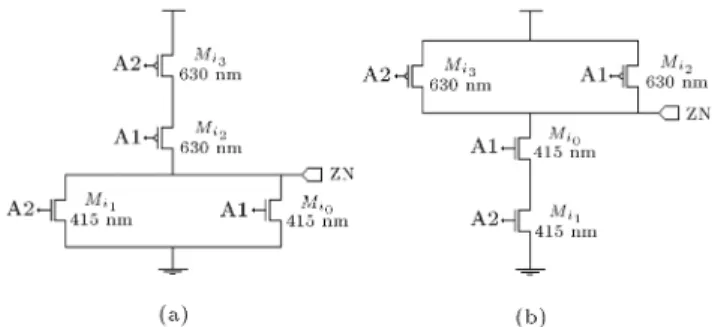
Various possible gate input vectors could result in various robustness levels of the gates. To investigate this issue, the output Qcirtof 2-input NAND and NOR
gates from Nangate open cell library [23] (Figure 2(a) and (b)) are indicated in Table 1. The gates are
Table 1. Qcirt(fc) vs. input for NAND2 and NOR2 gates of the employed cell library (VDD= 1:2 v).
Gateninput Qcirt(fc)
00 01 10 11
NAND2 9.9 5.62 5.56 6.92 NOR2 3.98 8.78 8.76 16.12
Figure 2. Transistor level schematic of a) NOR2, and b) NAND2 gates in Nangate open cell library.
employed from Nangate open cell library in 45-nm technology library.
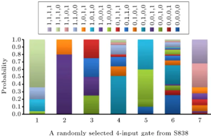
Various interconnection lines in a circuit have ei-ther a logic value of `1' or `0'. One of these values could have a higher probability of occurrence in comparison with the other. To conrm this issue, we selected twenty 2-input gates of benchmarks S838 and S526 on a random basis. Also, twenty 3-input gates as well as seven 4-input gates of the S838 benchmark circuits have been selected in the same way. As depicted in Figures 3-6, these gates, that have four/eight/sixteen possible input combinations, mainly have one or two of their possible input vectors with signicantly higher probability of occurrence in comparison with the other vectors. In this investigation, it is assumed that input SPs are 0.5 (the probability of having the logic value of `1'). For example, in circuit benchmark of S526, the
2-Figure 3. Input probability of 20 randomly selected 2-input gates from circuit S526.
Figure 4. Input probability of 20 randomly selected 2-input gates from circuit S838.
Figure 5. Input probability of 20 randomly selected 3-input gates from circuit S838.
Figure 6. Input probability of 4-input gates from circuit S838 assuming signal probability of 0.5 for circuit primary inputs.
input gate #1 has input vector of \10" in 90% of cases and has input vector of \00" only in 10%.
In benchmark circuit of S526, on average, the 2-input gates have one of their four possible 2-input vectors with probability of 72.9% (the maximum probability) and one other input combination with a probability of 3.26% (the minimum probability). Also, in the benchmark circuit of S838, on average, the 2-input gates have one of their four possible input vectors with probability of 66.8% (the maximum probability) and another with probability of 2.95% (the minimum probability).
This observation gave us this idea that, in order to improve the robustness of a gate against soft errors, it is not necessary to protect it for all cases of its inputs when some of them have a low or even zero probability of occurrence. Therefore, instead of upsizing all the transistors in a gate, we selectively enlarge only some of them and gain almost the same improvement in gate robustness.
In previously proposed gate resizing algorithms, in order to increase the Qcrit, mostly all transistors of
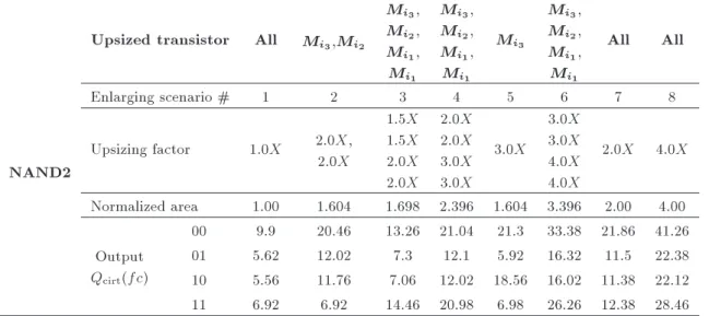
the selected gates were enlarged. Compared with our suggested method, this method can be considered as an area consuming method for SER reduction. As we have investigated for some gates of some evaluated bench-mark circuits, there is a low or even zero probability of occurrence for some input vectors. Therefore, for many of the gates, there is not such a need to enlarge all transistors of the gates. In Table 2, we showed the Qcirt of the output node of a NAND2 gate (shown in
Figure 2(a)) for its all four possible input combinations in 8 cases. In the rst case (enlarging scenario of #1), the transistors have their original sizes and in the other cases (as declared in the table), some of transistors are enlarged. In all the cases, the obtained improvement in critical charges is reported. As an example, we can suppose that a NAND2 gate has only two possible input vectors of \00" and \10". For this case, if we compare the enlarging scenarios of 2 and 5, we will nd that, although about 60% of original area has been added in both of these scenarios, there are larger Qcrits for input vectors of \00" and \10" in scenario
5. A similar Qcrits is also provided in scenario #7 in
which 100% area redundancy is imposed. This example shows us that we can selectively resize transistors of the gates considering their input vectors in such a way that the minimum area (and also delay) overhead being imposed.
In Figure 7, a rule for implementing the CATS idea is presented. This rule has a heuristic nature.
Generally, for every specic input, the ON tran-sistors should be enlarged. If the ON trantran-sistors are all PMOS, it is not needed to enlarge any of NMOS
Table 2. Output node Qcritof NAND2 gate of employed cell library for various scenarios of transistor resizing.
NAND2
Upsized transistor All Mi3,Mi2
Mi3,
Mi2,
Mi1,
Mi1
Mi3,
Mi2,
Mi1,
Mi1
Mi3
Mi3,
Mi2,
Mi1,
Mi1
All All
Enlarging scenario # 1 2 3 4 5 6 7 8
Upsizing factor 1:0X 2:0X, 2:0X
1:5X 1:5X 2:0X 2:0X
2:0X 2:0X 3:0X 3:0X
3:0X 3:0X 3:0X 4:0X 4:0X
2:0X 4:0X
Normalized area 1.00 1.604 1.698 2.396 1.604 3.396 2.00 4.00 Output
Qcirt(fc)
00 9.9 20.46 13.26 21.04 21.3 33.38 21.86 41.26 01 5.62 12.02 7.3 12.1 5.92 16.32 11.5 22.38 10 5.56 11.76 7.06 12.02 18.56 16.02 11.38 22.12 11 6.92 6.92 14.46 20.98 6.98 26.26 12.38 28.46
transistors. On the contrary, if there is any NMOS transistor between the ON transistors, its complemen-tary transistor should be enlarged as well.
Optimization 1: If there is a vector with probability higher than 80%, we only try for that input. For example, in a NAND2 gate, if there is an occurrence probability of 80% (or more) for input combination of \11", we only enlarge PMOS transistors instead of enlarging all 4 transistors. Therefore, if we double the PMOS sizes, we would save 20% of area budget for this gate (compared with the case of doubling all four transistors' sizes);
Optimization 2: We do not consider the input vectors with probability less than 20%;
Optimization 3: For some of the input vectors, it is not needed to enlarge even all the PMOS transistors and enlarging some of PMOSs (and not all) may result in the same robustness. For example, in a NAND2 gate, if there is a large probability for input \01", enlarging one of the PMOSs by 1:5X would give us higher robustness compared with enlarging both PMOSs by X (totally the increment would be 2X for both PMOSs). Furthermore, less area overhead would be imposed.
Figure 8. Proposed SET lter circuit.
3.2. Proposed LTD SET lter circuit
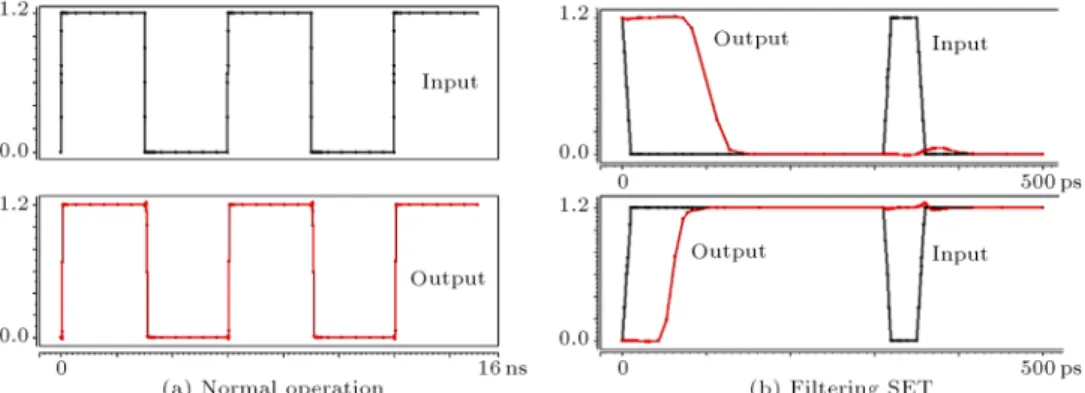
Our proposed SET lter circuit is shown in Fig-ure 8. Comparing this circuit with the ones proposed in [13,24], our simulation results show that our pro-posed circuit shows greater ability in SET ltering with the same area overhead. Also, this circuit has a lower propagation delay in comparison with them. In Table 3, a comparison has been made between our proposed circuit in this article and the ones proposed in [13,24]. In Figure 9, the LTD operation in normal mode (Figure 9(a)) and also in presence of SET pulse is shown (Figure 9(b)).
All the values in Table 3 are normalized to the related value of the proposed circuit in [24]. The rst column of the table shows propagation delay of the SET lter circuits and the second indicates
Table 3. Comparison of our proposed LTD SET lter with the proposed circuits in [13,24]. Circuit
Propagation delay (normalized)
Max. ltered SET pulse (normalized)
Area (normalized)
The proposed circuit in [24] 1.00 1.00 1.00
The proposed circuit in [13] 1.14 1.23 1.20
LTD with 1 TG 1.56 2.31 1.52
Figure 9. SET lter circuit in (a) normal operation, and (b) ltering SET.
the maximum SET pulse width that the circuits are capable of ltering out. Comparing our 1-TG LTD circuit with the one proposed in [24], our circuit has 56% more propagation delay while it is capable of ltering the SETs out with 131% larger pulse width. From Table 3, it is notable that two cascaded SET lters of [24] or [13] could lter normalized SET pulses of, respectively, 2.0 and 2.26 width, while our LTD circuit with two TGs can lter out a normalized SET pulse width of 3.69. It is also notable that, in these cases, our design has a normalized occupied area of 1.76, while the circuits represented in [24] and [13] have 2.0 and 2.4, respectively.
Our proposed LTD SET lter is tunable regard-less of transistor sizes. The circuit shown in Figure 8 includes two TG-gates; TG-0 and TG-1. We can justify the area, delay, and SET lter capability of our proposed circuit by varying the number of employed TGs. In Table 4, the propagation delay, maximum ltered SET pulse, and power consumption of our proposed LTD circuit versus number of its TGs are shown. All transistors have a minimum size, i.e. they are all sized with minimum applicable sizes in the employed library.
4. Proposed algorithms for soft error reduction and experimental results
In this section, we introduce three algorithms for SE protection. Algorithm-A employs only CATS
tech-nique and devotes the total area/timing budgets for this technique. Similarly, Algorithm-B dedicates all budgets for employing LTD circuits in various paths for removing the generated faulty pulses. Algorithm-C is a combination of Algorithm-A and Algorithm-B as the concluded algorithm. The impact of all three algorithms is evaluated via performed simulations. 4.1. Algorithm-A: Timing/area-aware
algorithm for gate resizing employing CATS
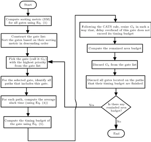
This algorithm considers both area and timing con-straints in employing the proposed CATS technique. This algorithm is presented in the following steps:
1. Constructions of gate list: Sort all gates based on their sorting metric in descending order (SM(Gk)):
SM(Gk) = SEPP(Gk)
X
i:all possible input vectors of gate Gk
Pi
1 Qcrit k i
all gates of the circuitAi P
j Aj
e Qcrit k iQs ; (3)
where SM(Gk) denotes the sorting metric of gate
Gk. SEPP(Gk) is soft error propagation
probabil-Table 4. Propagation delay, maximum ltered pulse width, and power consumption for various numbers of TGs. Number
of TGs
Propagation delay (ps)
Max. ltered
SET pulse (ps) Power (uW) Real Normalized Real Normalized Real Normalized
1 67 1.00 60 1.00 1.64 1.00
2 108 1.61 96 1.60 1.81 1.10
3 165 2.46 142 2.37 1.98 1.21
4 223 3.33 196 3.27 2.14 1.30
ity of Gk which is dened as the probability that
an SET originated at output of Gkgets to a
reach-able PO or FF. This parameter can be obtained using SER estimation technique proposed in [5]. Aiis drain area of the o-state transistor that was
hit. Qcrit k i is output critical charge of gate Gk
when it receives input vector i. Qs denotes the
charge slope which is discussed in detail in [25].
2. Pick the gate with the highest priority from the gate list (called Gk).
3. For the selected gate, identify all paths that contain this gate.
4. For all the paths, compute the average slack time (avg st(Pi)):
avg st(Pi) =dcritical pathn dpi
pi ; (4)
where, dcritical path, dpi, and npi denote delay of
critical path, delay of path Pi, and the number of
not resized gates in path Pi, respectively;
5. Compute the timing budget of the gate (tb(Gi)):
tb(Gk) =
minfavg st(Pi)gfor all associated paths of the gate Gk
max 8 > > > < > > > : 1 nP s;
SM(Gk) all not resized gates in the pathP
i SM(Gi)
9 > > > = > > > ; ; (5)
where nP sdenotes the number of not resized gates
in path Ps. The path Ps is the path that has the
minimum average slack time (avg st) among all paths consisted of gate Gk. It means that:
avg st(Ps)
= minfavg st(Pi)gfor all paths consisted of gate Gk:
6. Resize Gk in such a way that the delay overhead
of this gate does not exceed its timing budget (tb(Gk)). To resize the gate Gk, follow the CATS
rule represented in Figure 7.
7. Summate the imposed area overhead with previous area overheads and compute the remained area budget.
8. Discard the gate Gk from the gate list.
9. Check remained timing budget of all paths. For every path that its timing budget is nished, discard all its included gates from the gate list.
10. If there is any area budget, go back to step 2. Else, go to step 11.
11. End.
For the sake of clarity, this algorithm is repre-sented via a owchart in Figure 10.
To investigate the eect of the proposed algorithm on SER of the circuits, we performed a set of simula-tions to obtain the SEOR associated with each gate of some benchmark circuits. Also, the SEPP of each gate is obtained by the technique of [5]. To obtain the SEOR of each gate, the critical charge of each gate for all possible input vectors is achieved using the model presented in Eq. (1). Then, obtained critical charges were mapped to strike rate value of:
SEORGk =
all possible input vectorsX i
Pi F K
AAi
k e
Qcrit i k
Qs ; (6)
where, F denotes the particle ux with energy more than 10 Mev, K is a technology independent tting parameter, Piis the probability of input vector i, Ai is
drain area of the o-state transistor that was hit, Ak
is total area of gate Gk, and Qsis charge slope [25,26].
As we are interested in comparing the SER of some benchmark circuits after implementing our techniques with the state they had originally, we can normalize parameter SEOR to the metrics F and K. Therefore, we can re-write Eqs. (2) and then (6) as follow:
1
F K SEORGk=
all possible input vectors of GX k
i
Pi
Ai Ak e
Qcrit i k
Qs ; (7)
1
F K SERtotal=
all gates of the circuitX k
SEPPGk
SEOPGk; (8)
SERtotal-norm=
all gates of the circuitX k
SEPPGk
all possible input vectors of GX k
i
Pi
AAi
k e
Qcrit i k Qs
!
: (9)
To investigate the impact of our proposed CATS technique on SER and its eciency on cost overhead, we compared it with two other scenarios. Asadi and
Figure 10. The owchart of our proposed Algorithm-A.
Tahoori in [19], proposed an SER reduction technique as presented in the following (Algorithm-1):
Algorithm-1: At rst, they sort all gates based on their SEPP in decreasing order. Then, for the gate in list with highest priority, they enlarge the gate (enlarge all the transistors) by a factor of 4. Then, they check the timing and area budgets. This procedure will be continued while the timing and area budgets are not nished.
The second scenario considered for comparison is the following:
Algorithm-2: In this algorithm, we follow the steps of our proposed Algorithm-A with this dierence that in step 6, instead of our proposed CATS technique, we use the traditional transistor sizing approach. In other words, for resizing the selected gates, we simply enlarge all the transistors of the gates with no consideration regarding their inputs.
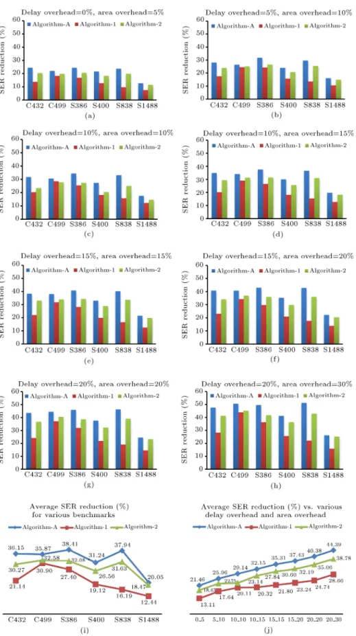
The simulation results for some benchmark cir-cuits in various cases of timing/area overhead are presented in Figure 11.
From the obtained results, it can be found that Algorithm-2 can reduce the SER of the circuits more
than Algorithm-1. It would be because it considers total SER instead of SEPP for sorting the gates. Moreover, as Algorithm-1 enlarges the gates by 4 orders of magnitude greedily, it can resize fewer numbers of gates before nishing its area budget. Our proposed algorithm (Algorithm-A) sorts the gates in terms of their total SER (instead of SEPP in Algorithm-1) and also considers input probability of the gates to resize them. As a result, it can aect the SER of the circuits with more eciency in comparison with Algorithm-1. Compared with 2, our proposed Algorithm-A considers input probability of the gates and resizes the transistors of the gate, selectively (instead of all transistors). For this reason, it generally can resize more numbers of gates in comparison with Algorithm-2 and therefore, it can reduce the total SER of the circuit more than Algorithm-2. In summary, it can be concluded that, our proposed algorithm (Algorithm-A) could reduce the SER of the circuits more than the two other considered algorithms.
4.2. Algorithm-B: Timing-aware algorithm for SET ltering using the proposed LTD circuit
In this scenario, we consider a timing budget in employing the LTD circuit. We insert an LTD circuit
Figure 11. Total SER reduction of our proposed Algorithm-A compared with Algorithm-1 and Algorithm-2 for various overheads of delay and area: a) 0% delay-5% area; b) 5% delay-10% area; c) 10% delay-10% area; d) 10% delay-15% area; e) 15% delay-15% area; f) 15% delay-20% area; g) 20% delay-20% area; h) 20% delay-30% area; i) average SER decrement for various benchmarks; and j) average SER decrement for various delay overheads and area overheads (the rst number is for delay and the second one is for area).
before every FFs or POs and tune it in a way that the timing budget is not exceeded. Using this technique, we reduce the probability of error propagation.
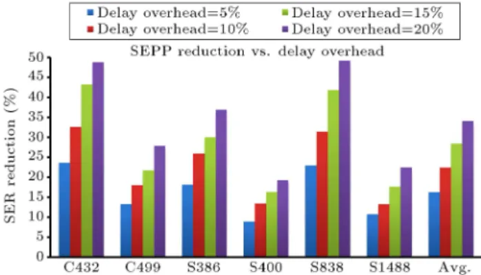
In Figure 12, the eect of this algorithm on SEPP reduction is investigated for some various benchmark circuits. In this gure, the SEPP reduction for various delay overheads is depicted. Moreover, In Figure 13, the area overhead imposed as result of this algorithm is shown. As can be found from the results, up to 50% SEPP reduction could be achieved using up to 30% area overhead and allowing delay overhead of 20%. Finally, in Figure 14, the eects of the proposed Algorithm-B on total SER reduction of the benchmarks are presented.
Figure 12. SEPP reduction of Algorithm-B versus various delay overheads.
Figure 13. Area overhead of Algorithm-B versus various delay overheads.
Figure 14. Total SER reduction of Algorithm-B versus various delay overheads.
As the results show, on average, about 22% reduction in total SER of the benchmark circuit is achieved with imposing 20% delay overhead in Algorithm-B.
4.3. Algorithm-C: Timing/area-aware algorithm for combining gate resizing employing CATS and SET ltering employing proposed LTD circuit
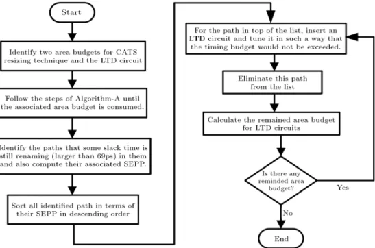
In Algorithm-A, we considered two constraints of area and timing together. During the performed simulations regarding implementation of Algorithm-A, we noticed that, in most cases, the area budget was nished whilst some timing budgets were still unused. Also, in Algorithm-B, inserting an LTD circuit before all POs/FFs imposes less than 10% area overhead in many of the benchmark circuits. The key idea behind the 3rd algorithm (Algorithm-C) is re-using the remaining tim-ing budgets after employtim-ing Algorithm-A by enhanctim-ing the paths with remaining slack time higher than 67 ps (the propagation delay of the LTD circuit, tuned with one TG) with an LTD circuit.
In Algorithm-C, we consider two area budgets for both the CATS resizing technique and LTD circuit employing. This algorithm can be pursued by the following steps:
1. Follow the steps of Algorithm-A until the associated area budget is consumed;
2. Identify the paths in which some slack time is still remained (larger than 69ps) for them, and also compute their associated SEPP;
3. Sort all identied paths in terms of their SEPP in descending order;
4. For the path in top of the list, insert an LTD circuit and tune it in such a way that the timing budget would not be exceeded;
5. Eliminate this path from the list;
6. Calculate the remained area budget for LTD cir-cuits;
7. If there is still some area budget, go back to step 4, else go to step 8.
8. End.
These steps are also presented in the depicted owchart of Figure 15.
The simulation results regarding Algorithm-C are presented in Figure 16. In all cases of these results, 70% of area budget is devoted to transistor resizing and the rest 30% to inserting the proposed LTD circuit. As can be found from the results, with more overhead of area and delay, the proposed Algorithm-C can achieve more decrement in SER reduction of the circuit in comparison with Algorithm-A (Figure 16(d)).
Figure 15. The owchart of our proposed Algorithm-C.
Figure 16. Total SER decrement of Algorithm-C in comparison with Algorithm-A for various delay and area overheads: a) 0% dely-5% area; b) 10% delay-15% area; c) 15% delay-20% area; d) 20% delay-30% area; e) average SER reduction for various benchmark circuits; and f) average SER reduction for various delay overheads and area overheads (the rst number is for delay and the second one is for area).
5. Conclusion
In this article, two soft error protection techniques were proposed. One of these techniques, that is a new cost aware gate re-sizing method, tries to reduce SEOR in combinational logic and the other, that is an SET lter circuit, tries to avoid the propagation of SEs in combinational logic. We also proposed three algorithms for SER reduction in combinational logic that employ our proposed gate sizing method and SET lter circuit. Various simulation results for dierent scenarios were presented and showed that our proposed algorithms have more eciency and also eect more on SER reduction in comparison with some other algorithms and techniques. The simulation results show that, at the expense of 20% delay and also 30% area overhead, up to 70% reduction in total SER is obtained by our nal proposed algorithm (Algorithm-C), that combines our proposed CATS technique and uses our proposed LTD SET lter circuit.
References
1. Rajaei, R., Tabandeh, M. and Rashidian, B. \Single event upset immune latch circuit design Using C-element", The IEEE 9th International Conference on ASIC (ASICON2011), Xiamen, China (25-28 Oct., 2011).
2. Rajaei, R., Tabandeh, M. and Fazeli, M. \Low cost soft error hardened latch designs for nano-scale cmos technology in presence of process variation", Micro-electronic Reliability, Elsevier (2013).
3. Fazeli, M., Miremadi, S.G., Asadi, H. and Ahmadian, S.N. \A fast and accurate multi-cycle soft error rate estimation approach to resilient embedded systems de-sign", The 40th Annual IEEEIFIP International Con-ference on Dependable Systems and Networks (DSN 2010), Chicago, USA (28 June-1 July, 2010).
4. Ahlbin, J.R., Gadlage, M.J., Atkinson, N.M., Narasimham, B., Bhuva, B.L., Witulski, A.F., Tim-othy Holman, W., Eaton, P.H. and Massengill, L.W. \Eect of multiple-transistor charge collection in single-event transient pulse widths", IEEE Transac-tion on Device and Material reliability, 11(3), pp. 401-406 (2011).
5. Rajaei, R., Tabandeh, M. and Fazeli, M. \Soft error rate estimation for combinational logic in presence of single event multiple transients", Journal of Circuits, Systems, and Computers, World Scientic, 23(6), 1450091-1 to 1450091-20 (20 pages) (2014).
6. Messenger, G.C. \Collection of charge on junction nodes from ion tracks", IEEE Trans. Nuclear Science, NS-29, pp. 2024-2031 (Dec. 1982).
7. Zhou, Q. and Mohanram, K. \Gate sizing to radia-tion harden combinaradia-tional logic", IEEE Transacradia-tions on Computer-Aided Desing of Integrated Circuits and Systems, 25(1), pp. 155-166 (Jan. 2006).
8. Asadi, H., Tahoori, M., Fazeli, M. and Miremadi, S.G. \Ecient algorithms to accurately compute derating factors of digital circuits", Elsevier Microelectronics Reliability (2012).
9. Asadi, G. and Tahoori, M.B. \An accurate ser es-timation method based on propagation probability", In Proceedings of the IEEE/ACM International Con-ference on Design, Automation and Test in Europe (DATE), pp. 306-7 (March 2005).
10. Asadi, G. and Tahoori, M.B. \An analytical approach for soft error rate estimation in digital circuits", In Proceedings of the IEEE International Symposium on Circuits and Systems (ISCAS), 3, pp. 2991-4 (May 2005).
11. Ebrahimi, M., Asadi, H. and Tahoori, M.B. \A layout-based approach for multiple event transient analysis", In Proceedings of 50th Design Automation Conference (DAC), USA (2013).
12. Fazeli, M. and Miremadi, S.G. \A power ecient masking technique for design of robust embedded systems against SEUs and SETs", IEEE International Symposium on Defect and Fault Tolerance of VLSI Systems (2010).
13. Bhattacharya, K. and Ranganathan, N. \RADJAM: A novel approach for reduction of soft errors in logic circuits", In Proceedings of 22nd International Confer-ence on VLSI Design, pp. 453-458, New Delhi, India (Jan. 2009).
14. Sootkaneung, W. and Saluja, K.K. \Gate input re-conguration for combating soft errors in combina-tional circuits", in Proceedings of Internacombina-tional Confer-ence on Dependable Systems and Networks Workshops (DSN-W'10), pp. 107-112, Chicago, USA (July 2010).
15. Almukhaizim, S. and Makris, Y. \Soft error mitigation through selective addition of functionally redundant wires", IEEE Transactions on Reliability, 57(1), pp. 23-31 (March 2008).
16. Ding, Q., Wang, Y., Wang, H., Luo, R. and Yang, H. \Output remapping technique for critical paths soft-error rate reduction", In Proceedings of Computers & Digital Techniques (IET'10), pp. 325-333, London, UK (Nov. 2010).
17. Sootkaneung, W. and Saluja, K.K. \Soft error reduc-tion through gate input dependent weighted sizing in combinational circuits", In Proceedings of the 12th International Symposium on Quality Electronic Design (ISQED 2011), Santa Clara, CA (2011).
18. Sootkaneung, W. and Saluja, K.K. \Optimizing de-vice size for soft error resilience in sub-micron logic circuits", In Proceedings of the 2nd Asia Symposium on Quality Electronic Design (ASQED 2010), Penang, Malaysia, pp. 235-242 (2010).
19. Asadi, H. and Tahoori, M.B. \Soft error modeling and remediation techniques in ASIC designs", Elsevier Journal of Microelectronics Engineering, 41(8), pp. 506-522 (Aug. 2010).
20. Rao, R.R., Blaauw, D. and Sylvester, D. \Soft error reduction in combinational logic using gate resizing and lipop selection", In Proceedings of IEEE/ACM International Conference on Computer-Aided Design, pp. 502-509, San Jose, USA (Nov. 2006).
21. Sheng, W., Xiao, L. and Mao, Z. \Soft error opti-mization of standard cell circuits based on gate sizing and multi-objective genetic algorithm", In Proceedings of Design Automation Conference (DAC'09), pp. 502-507, San Francisco, USA (July 2009).
22. Zhou, Q. and Mohanram, K. \Transistor sizing for radiation hardening", In Proceedings of the Interna-tional Reliability Physics Symposium (IRPS), pp. 310-315 (2004).
23. http://www.nangate.com
24. Sasaki, Y., Namba, K. and Ito, H. \Soft error mask-ing circuit and latch usmask-ing Schmitt trigger circuit", In Proceedings of IEEE International Symposium on Defect and Fault Tolerance in VLSI Systems, pp. 327-335, Arlington, USA (Oct. 2006).
25. Hazucha, P. and Svensson, C. \Impact of CMOS technology scaling on the atmospheric neutron soft error rate", IEEE Transactions on Nuclear Science, 47(06), pp. 2586-2594 (Dec. 2000).
26. Rajaei, R., Fazeli, M. and Tabandeh, M. \Soft error-tolerant design of MRAM-based non-volatile latches for sequential logics", IEEE Transaction on Magnetics (2014).
Biographies
Ramin Rajaei received his MSc and PhD degrees in Electrical Engineering/Digital Electronics from Sharif University of Technology (SUT) in 2009 and 2014,
respectively. In Fall 2015, he joined the Department of Electrical Engineering, Shahid Beheshti University (SBU) as an Assistant Professor. His research interests include reliability issues in VLSI circuits and emerging technologies (soft errors, process variation, aging), reliability modeling/estimation, and fault tolerant em-bedded system design.
Mahmoud Tabandeh received his Engineering Diploma in Electronics from INSA, Lyon, France, in 1967, MS degree in Control Systems from LSU, Baton Rouge, Louisiana, in 1969, and PhD degree in Computer Hardware from the University of California, Berkley, in 1974. He is currently an Associate Professor at the Department of Electrical Engineering, Sharif University of Technology, Tehran, Iran. His research interests include digital systems, hardware and soft-ware in general, and image and video processing in particular.
Mahdi Fazeli received the MSc and PhD degrees in Computer Engineering from Sharif University of Technology, Tehran, Iran, in 2005 and 2011, respec-tively. He has been working at the Department of Computer Engineering, Iran University of Science and Technology (IUST), since 2011, where he is currently an Assistant Professor. He has established and chaired the Dependable Systems and Architectures Laboratory (DSA Lab) at IUST, since 2012. His current research interests include reliable issues in VLSI circuits and emerging technologies, dependable embedded systems, Low power circuits and systems, fault-tolerant com-puter architectures, and reliability modeling and eval-uation.