1
1060fb
Universal Dual Filter
Building Block
DESCRIPTIO
U
APPLICATIO S
U
■ Guaranteed Filter Specification for ±2.37V and
±5V Supply
■ Operates Up to 30kHz
■ Low Power and 88dB Dynamic Range at ±2.5V Supply
■ Center Frequency Q Product Up to 1.6MHz
■ Guaranteed Offset Voltages
■ Guaranteed Clock-to-Center Frequency Accuracy Over
Temperature:
0.3% for LTC1060A 0.8% for LTC1060
■ Guaranteed Q Accuracy Over Temperature
■ Low Temperature Coefficient of Q and Center
Frequency
■ Low Crosstalk, 70dB
■ Clock Inputs TTL and CMOS Compatible
■ Single 5V Supply Medium Frequency Filters
■ Very High Q and High Dynamic Range Bandpass,
Notch Filters
■ Tracking Filters
■ Telecom Filters
Single 5V, Gain of 1000 4th Order Bandpass Filter
The LTC®
1060 consists of two high performance, switched capacitor filters. Each filter, together with 2 to 5 resistors, can produce various 2nd order filter functions such as lowpass, bandpass, highpass notch and allpass. The center frequency of these functions can be tuned by an external clock or by an external clock and resistor ratio. Up to 4th order full biquadratic functions can be achieved by cascading the two filter blocks. Any of the classical filter configurations (like Butterworth, Chebyshev, Bessel, Cauer) can be formed.
The LTC1060 operates with either a single or dual supply
from ±2.37V to ±8V. When used with low supply
(i.e. single 5V supply), the filter typically consumes 12mW and can operate with center frequencies up to 10kHz. With
±5V supply, the frequency range extends to 30kHz and
very high Q values can also be obtained.
The LTC1060 is manufactured by using Linear Technology’s enhanced LTCMOS™ silicon gate process. Because of this, low offsets, high dynamic range, high center frequency Q product and excellent temperature stability are obtained.
The LTC1060 is pinout compatible with MF10.
FEATURES
TYPICAL APPLICATIO
U
Amplitude Response LTC1060 • TA01 VIN 1mV(RMS) 0.1µF 3.16k 3.16k 100k 2k 100k LTC1060 2k 1 2 3 4 5 6 7 8 9 10 20 19 18 17 16 15 14 13 12 11 5V 5V OUTPUT 1k 1k CLOCK IN 17.5kHz INPUT FREQUENCY (Hz) 0 GAIN (dB) 30 50 275 LTC1060 • TA02 10 –10 125 175 225 100 150 200 250 70 20 40 0 60, LTC and LT are registered trademarks of Linear Technology Corporation. LTCMOS trademark of Linear Technology Corporation.
2
1060fb ORDER PART NUMBER LTC1060ACN LTC1060CN LTC1060CSW LTC1060ACJ LTC1060MJ LTC1060AMJ LTC1060CJ TOP VIEW J PACKAGE 20-LEAD CERDIP TJMAX = 150°C, θJA = 70°C/W TJMAX = 100°C, θJA = 100°C/W (N) 1 2 3 4 5 6 7 8 9 20 19 18 17 16 15 14 13 12 11 LPA BPA N/AP/HPA INVA S1A SA/B VA+ VD+ LSh CLKA LPB BPB N/AP/HPB INVB S1B AGND VA– VD– 50/100/HOLD CLKB 10 N PACKAGE 20-LEAD PDIP SW PACKAGE 20-LEAD PLASTIC SO WIDETJMAX = 150°C, θJA = 80°C/W (SW)
Supply Voltage ... 18V Power Dissipation ... 500mW Operating Temperature Range
LTC1060AC/LTC1060C ... – 40°C ≤ TA≤ 85°C
LTC1060AM/LTC1060M ... – 55°C ≤ TA≤ 125°C
Storage Temperature Range ... – 65°C to 150°C
Lead Temperature (Soldering, 10 sec)... 300°C
Consult LTC Marketing for parts specified with wider operating temperature ranges.
(Note 1)
OBSOLETE PACKAGE
Consider the N20 and SW20 Package for Alternate SourceABSOLUTE AXI U RATI GS
W
W
W
U
PACKAGE/ORDER I FOR ATIO
U
W
U
The ● denotes specifications which apply over the full operating
temperature range, otherwise specifications are at TA = 25°C. (Complete Filter) Vs = ±5V, unless otherwise noted.
ELECTRICAL CHARACTERISTICS
PARAMETER CONDITIONS MIN TYP MAX UNITS
Center Frequency Range f0 • Q ≤ 400kHz, Mode 1, Figure 4 0.1 to 20k Hz
(See Applications Information) f0 • Q ≤ 1.6MHz, Mode 1, Figure 4 0.1 to 16k Hz
Clock-to-Center Frequency Ratio
LTC1060A Mode 1, 50:1, fCLK = 250kHz, Q = 10 ● 50 ± 0.3% LTC1060 Mode 1, 50:1, fCLK = 250kHz, Q = 10 ● 50 ± 0.8% LTC1060A Mode 1, 100:1, fCLK = 500kHz, Q = 10 ● 100 ± 0.3% LTC1060 Mode 1, 100:1, fCLK = 500kHz, Q = 10 ● 100 ± 0.8% Q Accuracy LTC1060A Mode 1, 50:1 or 100:1, f0 = 5kHz, Q=10 ● ±0.5 3 % LTC1060 Mode 1, 50:1 or 100:1, f0 = 5kHz, Q=10 ● ±0.5 5 %
f0 Temperature Coefficient Mode 1, fCLK < 500kHz –10 ppm/°c
Q Temperature Coefficient Mode 1, fCLK < 500kHz, Q = 10 20 ppm/°c
DC Offset VOS1 ● 2 15 mV
VOS2 fCLK = 250kHz, 50:1, SA/B = High ● 3 40 mV
VOS2 fCLK = 500kHz, 100:1, SA/B = High ● 6 80 mV
VOS2 fCLK = 250kHz, 50:1, SA/B = Low ● 2 30 mV
VOS2 fCLK = 500kHz, 100:1, SA/B = Low ● 4 60 mV
VOS3 fCLK = 250kHz, 50:1, SA/B = Low ● 2 30 mV
VOS3 fCLK = 500kHz, 100:1, SA/B = Low ● 4 60 mV
DC Lowpass Gain Accuracy Mode 1, R1 = R2 = 50k ±0.1 2 %
BP Gain Accuracy at f0 Mode 1, Q = 10, f0 = 5kHz ±0.1 %
Clock Feedthrough fCLK≤ 1MHz 10 mV(P-P)
Max Clock Frequency 1.5 MHz
Power Supply Current 3 5 8 mA
● 12 mA
3
1060fb
The ● denotes specifications which apply over the full operating temperature
range, otherwise specifications are at TA = 25°C. (Complete Filter) VS = ±2.37V.
ELECTRICAL CHARACTERISTICS
Note 1: Absolute Maximum Ratings are those values beyond which the life of a device may be impaired.
PARAMETER CONDITIONS MIN TYP MAX UNITS
Center Frequency Range f0 • Q ≤ 100kHz 0.1 to 10k Hz
Clock-to-Center Frequency Ratio
LTC1060A Mode 1, 50:1, fCLK = 250kHz, Q = 10 ● 50 ± 0.5% LTC1060 Mode 1, 50:1, fCLK = 250kHz, Q = 10 50 ± 0.8% LTC1060A Mode 1, 100:1, fCLK = 250kHz, Q = 10 ● 100 ± 0.5% LTC1060 Mode 1, 100:1, fCLK = 250kHz, Q = 10 100 ± 0.8% Q Accuracy LTC1060A Mode1, 50:1 or 100:1, f0 = 2.5kHz, Q = 10 ±2 % LTC1060 Mode1, 50:1 or 100:1, f0 = 2.5kHz, Q = 10 ±4 %
Max Clock Frequency 500 kHz
Power Supply Current 2.5 4 mA
The ● denotes specifications which apply over the full operating temperature range, otherwise specifications are at TA = 25°C.
(Internal Op Amps).
PARAMETER CONDITIONS MIN TYP MAX UNITS
Supply Voltage Range ±2.37 ±8 V
Voltage Swings
LTC1060A ±4 ±4 V
LTC01060 VS = ±5V, RL = 5k (Pins 1,2,19,20) ±3.8 ±4 V
LTC01060, LTC01060A RL = 3.5k (Pins 3,18) ● ±3.6 ±4 V
Output Short-Circuit Current VS = ±5V
Source 25 mA
Sink 3 mA
Op Amp GBW Product VS = ±5V 2 MHz
Op Amp Slew Rate VS = ±5V 7 V/µs
Op Amp DC Open Loop Gain RL = 10k, VS = ±5V 85 dB
AGND TO AGND INVB CLKA CLKB 50/100/HOLD LEVEL SHIFT S2A S2B INVA + – – + – – LTC1060 • BD01 + – + – LEVEL SHIFT NON-OVERLAP CLOCK LEVEL SHIFT NON-OVERLAP CLOCK CONTROL 17 11 9 12 10 15 4 VD+ VA+ N/AP/HPAS1A BPA LPA 8 7 3 5 2 1 VD– VA– 14 13 18 19 20 BPB LPB N/AP/HPBS1B 16 SAB 6 ∑ ∑ ∫ ∫ ∫ ∫
BLOCK DIAGRA
W
4
1060fb Graph 1. Mode 1: (fCLK/f0) Deviation vs Q Graph 2. Mode 1: (fCLK/f0) Deviation vs Q Graph 3. Mode 1:Q Error vs Clock Frequency
Graph 7. Mode 1: (fCLK/f0) vs fCLK and Q IDEAL Q 0.1 –1.6 % DEVIATION ( fCLK /f0 ) –1.2 –0.8 –0.4 0 1 10 100 LT1060 • TPC01 –2.0 –2.4 0.4 VTSA = = 25±5V°C fCLK = 250kHz = 50 (TEST POINT) fCLK f0 IDEAL Q 0.1 – 0.3 % DEVIATION ( fCLK /f0 ) – 0.2 – 0.1 0 0.1 1 10 100 LT1060 • TPC02 – 0.4 – 0.5 – 0.6 fCLK = 100 (TEST POINT) fCLK f0 VS = ±5V TA = 25°C fCLK = 500kHz fCLK (MHz) 0.2 0
DEVIATION FROM IDEAL Q (%) 10
0 10 20 0.6 1.0 1.2 2.0 LTC1060 • TPC03 20 0.4 0.8 1.4 1.6 1.8 = 50:1 fCLK f0 = 100:1 fCLK f0 VS = ±2.5V TA = 25°C VS = ±2.5V VS = ±5V VS = ±5V 50 2010 10 20 50 100 Q = 5 100 20 10 20 Q = 5 50 10 Q = 5 Q = 5 50 = 50:1 fCLK f0 VS= ±5V TA = 25°C fCLK (MHz) 0 DEVIATION FROM 50:1 (%) 0.4 0.6 0.8 0.6 1.0 LTC1060 • TPC07 0.2 0 0.2 0.4 0.8 1.2 1.4 –0.2 –0.4 Q = 50 Q = 5 Q = 10 Q = 20
TYPICAL PERFOR A CE CHARACTERISTICS
W
U
Graph 4. Mode 1:
Q Error vs Clock Frequency
Graph 5. Mode 1: Measured Q vs
fCLK and Temperature Graph 6. Mode 1: (fCLK/f0) vs fCLK and Q Graph 8. Mode 1: (fCLK/f0) vs fCLK and Temperature Graph 9. Mode 1: (fCLK/f0) vs fCLK and Temperature fCLK (MHz) 0.2 0
DEVIATION FROM IDEAL Q (%) 10
0 200 50 10 20 0.6 1.0 1.2 2.0 LTC1060 • TPC04 20 0.4 0.8 1.4 1.6 1.8 = 50:1 fCLK f0 = 100:1 fCLK f0 VS = ±7.5V TA = 25°C 400 200 100 10 Q = 5 50 400 100 Q = 5 10 = 50:1 fCLK f0 = 100:1 fCLK f0 VS= ±5V Q = 10 fCLK (MHz) 0.2 –20
DEVIATION FROM IDEAL Q (%) 0
20 0 0.6 1.0 1.4 1.8 LTC1060 • TPC05 20 0.4 0.8 1.2 1.6 85°C 125°C 85°C 125°C –55°C – 55°C TA = 25°C TA = 25°C = 100:1 fCLK f0 VS= ±5V TA = 25°C fCLK (MHz) 0 DEVIATION FROM 100:1 (%) 0.4 0.6 0.8 0.6 1.0 LTC1060 • TPC06 0.2 0 0.2 0.4 0.8 1.2 1.4 –0.2 –0.4 Q = 50 Q = 5 Q = 10 Q = 20 fCLK (MHz) 0.2 –0.2 DEVIATION FROM 100:1 (%) 0 0.2 0.6 0.6 1.0 1.4 1.8 LTC1060 • TPC08 0.8 0.4 1.0 0.4 0.8 1.2 1.6 85°C TA = 25°C 125°C fCLK f0 = 100:1 VS= ±5V Q = 10 –55°C fCLK (MHz) 0.2 –0.2 DEVIATION FROM 50:1 (%) 0 0.2 0.6 0.6 1.0 1.4 1.8 LTC1060 • TPC09 0.8 0.4 1.0 0.4 0.8 1.2 1.6 fCLK f0 = 50:1 VS= ±5V Q = 10 –55°C TA= 25°C 85°C 125°C
5
1060fb Graph 10. Mode 1: (fCLK/f0) vs fCLK and Q Graph 11. Mode 1: (fCLK/f0) vs fCLK and Q Graph 12. Mode 1: (fCLK/f0) vs fCLK and Temperature Graph 13. Mode 1: (fCLK/f0) vs fCLK and Temperature Graph 14. Mode 1:Notch Depth vs Clock Frequency
Graph 15. Mode 3: Deviation of
(fCLK/f0) with Respect to Q = 10
Measurement
Graph 16. Mode 3: Q Error vs Clock Frequency
Graph 17. Mode 3 (R2 = R4): Q Error vs Clock Frequency
Graph 18. Mode 3 (R2 = R4): Measured Q vs fCLK and Temperature = 100:1 fCLK f0 VS= ±2.5V TA = 25°C fCLK (MHz) 0 DEVIATION FROM 100:1 (%) 0.6 0.8 1.0 300 500 LTC1060 • TPC10 0.4 0.2 100 200 400 600 700 0 –0.2 Q = 50 Q = 5 Q = 20 Q = 10 = 50:1 fCLK f0 VS= ±2.5V TA = 25°C fCLK (MHz) 0 DEVIATION FROM 50:1 (%) 0.4 0.6 0.8 300 500 LTC1060 • TPC11 0.2 0 100 200 400 600 700 – 0.2 –0.4 Q = 5 Q = 10 Q = 20 Q = 50 fCLK (kHz) 0 DEVIATION FROM 100:1 (%) 0 0.2 0.4 0.6 1 0.2 0.4 0.6 0.8 LTC1060 • TPC12 1.0 1.2 0.8 = 100:1 fCLK f0 VS= ±2.5V Q = 10 –55°C TA = 25°C 85°C 125°C fCLK (kHz) 0 DEVIATION FROM 50:1 (%) 0 0.2 –0.2 0.4 0.6 1.0 0.2 0.4 0.6 0.8 LTC1060 • TPC13 1.0 1.2 0.8 = 50:1 fCLK f0 VS= ±2.5V Q = 10 –55°C TA = 25°C 85°C 125°C fCLK (MHz) 0 0 NOTCH DEPTH (dB) 20 40 60 80 0.4 0.8 1.2 1.6 LTC1060 • TPC14 100 120 0.2 0.6 1.0 1.4 VS= ±5V TA = 25°C VIN = 1VRMS Q = 10 100:1 Q = 1 100:1 Q = 10 50:1 IDEAL Q (A) (B) 0.1 –0.2 Q = 10 MEASUREMENT (%) DEVIATION OF fCLK fO WITH RESPECT TO –0.1 0 0.1 1 10 100 LTC1060 • TPC15 –0.3 –0.4 –0.5 = 500: 1 fCLK fO R2 = R4 1 5 = 200: 1 fCLK fO R2 = R4 1 2 VS= ±5V TA = 25°C PIN 12 AT 100:1 fCLK (MHz) 0.2 0 Q ERROR (%) 10 0 10 20 0.6 1.0 1.2 2.0 LTC1060 • TPC17 20 0.4 0.8 1.4 1.6 1.8 = 100:1 fCLK f0 VS = ±7.5V TA = 25°C Q = 5 Q = 5 50 = 50:1 50 10 10 fCLK f0 = 50:1 fCLK f0 = 100:1 fCLK f0 VS= ±5V Q = 10 fCLK (MHz) 0.2 –20
DEVIATION FROM IDEAL Q (%) 0
20 0 0.6 1.0 1.4 1.8 LTC1060 • TPC18 20 40 –20 40 0.4 0.8 1.2 1.6 –55°C –55°C 125°C 85°C TA = 25°C 125°C 85°C TA = 25°C fCLK (MHz) 0.2 0
DEVIATION FROM IDEAL Q (%) 10
0 10 20 0.6 1.0 1.2 2.0 LTC1060 • TPC16 20 0.4 0.8 1.4 1.6 1.8 = 50:1 fCLK f0 = 100:1 fCLK f0 TA = 25°C 10 20 20 50 Q = 5 Q = 5 Q = 5 20 20 10 10 VS = ±2.5V VS = ±5V VS = ±2.5V VS = ±5V 50 50 Q = 5 10 50
6
1060fb Graph 19. Mode 3 (R2 = R4): (fCLK/f0) vs fCLK and Q Graph 20. Mode 3 (R2 = R4): (fCLK/f0) vs fCLK and Q Graph 21. Mode 3 (R2 = R4): (fCLK/f0) vs fCLK and Temperature Graph 22. Mode 3 (R2 = R4): (fCLK/f0) vs fCLK and Temperature Graph 23. Mode 3 (R2 = R4): (fCLK/f0) vs fCLK and Temperature Graph 24. Mode 3 (R2 = R4): (fCLK/f0) vs fCLK and Temperature Graph 25. Mode 1c (R5 = 0), Mode 2 (R2 = R4) Q Error vs Clock FrequencyGraph 26.Supply Current vs Supply Voltage = 100:1 fCLK f0 VS= ±5V TA = 25°C fCLK (MHz) 0 DEVIATION FROM 100:1 (%) 0.4 0.6 0.8 0.6 1.0 LTC1060 • TPC19 0.2 0 0.2 0.4 0.8 1.2 1.4 –0.2 –0.4 Q = 20, Q = 40, Q = 50 Q = 5 Q = 10 = 50:1 fCLK f0 VS= ±5V TA = 25°C fCLK (MHz) 0 DEVIATION FROM 50:1 (%) 0.4 0.6 0.8 0.6 1.0 LTC1060 • TPC20 0.2 0 0.2 0.4 0.8 1.2 1.4 –0.2 –0.4 Q = 10 Q = 5 Q = 50 Q = 20 = 100:1 fCLK f0 VS= ±5V Q = 10 fCLK (MHz) 0.2 –0.2 DEVIATION FROM100:1 (%) 0 0.2 0.6 0.6 1.0 1.4 1.8 LTC1060 • TPC21 0.8 0.4 1.0 0.4 0.8 1.2 1.6 85°C 125°C TA = 25°C –55°C = 100:1 fCLK f0 VS= ±5V Q = 10 fCLK (MHz) 0.2 DEVIATION FROM 50:1 (%) 0 0.2 0.6 0.6 1 1.4 1.8 LTC1060 • TPC22 0.8 0.4 1.0 0.4 0.8 1.2 1.6 85°C –55°C 125°C TA = 25°C fCLK (MHz) 0 DEVIATION FROM 100:1 (%) –0.2 –0.4 0 0.2 0.4 0.8 0.2 0.4 0.6 0.8 LTC1060 • TPC23 1.0 1.2 0.6 = 100:1 fCLK f0 VS= ±2.5V Q = 10 –55°C TA = 25°C 85°C 125°C fCLK (MHz) 0 DEVIATION FROM 50:1 (%) 0 0.2 0.4 0.6 1.0 0.2 0.4 0.6 0.8 LTC1060 • TPC24 1.0 0.8 = 100:1 fCLK f0 VS= ±2.5V Q = 10 – 55°C TA = 25°C 85°C 125°C fCLK f0 70.7 1 fCLK f0 35.37 1 VS= ±5V TA = 25°C fCLK (MHz) 0
DEVIATION FROM IDEAL Q (%)
10 20 0.6 1.0 LTC1060 • TPC25 0 20 0.2 0.4 0.8 1.2 1.4 10 0 MODE 2 R2 = R4 = Q = 10 Q = 10 Q = 20 Q = 20 MODE 2 R2 = R4 20 20 SUPPLY VOLTAGE (±V) 0 2 4 6 8 10 12 14 16 18 20
SUPPLY CURRENT (mA)
±3 ±5 ±7 ±9 LTC1060 • TPC26 ±11 ±2 ±1 ±4 ±6 ±8 ±10 fCLK ≤ 1MHz TA = –55°C TA = 25°C TA = 125°C
7
1060fb
operation of the device. By tying Pin 12 to 1/2 supplies (which should be the AGND potential), the LTC1060 operates in the 100:1 mode. The 1/2 supply bias of Pin 12 can vary around the 1/2 supply potential without affecting the 100:1 filter operation. This is shown in Table 1. When Pin 12 is shorted to the negative supply pin, the filter operation is stopped and the bandpass and lowpass outputs act as a S/H circuit holding the last sample. The
hold step is 20mV and the droop rate is 150µV/second!
Table 1
VOLTAGE RANGE OF PIN 12
TOTAL POWER SUPPLY FOR 100:1 OPERATION
5V 2.5 ± 0.5V
10V 5V ± 1V
15V 7.5V ± 1.5V
S1A, S1B (Pins 5 and 16)
These are voltage signal input pins and, if used, they
should be driven with a source impedance below 5kΩ. The
S1A, S1B pins can be used to alter the CLK to center
frequency ratio (fCLK/f0) of the filter (see Modes 1b, 1c, 2a,
2b) or to feedforward the input signal for allpass filter configurations (see Modes 4 and 5). When these pins are not used, they should be tied to the AGND pin.
SA/B (Pin 6)
When SA/B is high, the S2 input of the filter’s voltage
summer (see Block Diagram) is tied to the lowpass output. This frees the S1 pin to realize various modes of operation
for improved applications flexibility. When the SA/B pin is
connected to the negative supply, the S2 input switches to ground and internally becomes inactive. This improves the filter noise performance and typically lowers the value
of the offset VOS2.
AGND (Pln 15)
This should be connected to the system ground for dual supply operation. When the LTC1060 operates with a single positive supply, the analog ground pin should be
tied to 1/2 supply and bypassed with a 0.1µF capacitor, as
shown in the application, “Single 5V, Gain of 1000 4th Order Bandpass Filter.” The positive inputs of all the
Power Supplies
The V+A and V+D (pins 7 and 8) and the V–A and V–D
(Pins 14 and 13) are, respectively, the analog and digital positive and negative supply pins. For most cases, Pins 7
and 8 should be tied together and bypassed by a 0.1µF disc
ceramic capacitor. The same holds for Pins 13 and 14. If the LTC1060 operates in a high digital noise environment, the supply pins can be bypassed separately. Pins 7 and 8 are internally connected through the IC substrate and should be biased from the same DC source. Pins 13 and 14 should also be biased from the same DC source.
The LTC1060 is designed to operate with ±2.5V supply
(or single 5V) and with ±5V to ±8V supplies. The
mini-mum supply, where the filter operates reliably, is ±2.37V.
With low supply operation, the maximum input clock frequency is about 500kHz. Beyond this, the device exhib-its excessive Q enhancement and center frequency errors.
Clock Input Pins and Level Shift
The level shift (LSh) Pin 9 is used to accommodate T2L or
CMOS clock levels. With dual supplies equal or higher
to ±4.5V, Pin 9 should be connected to ground (same
potential as the AGND pin). Under these conditions the
clock levels can be T2L or CMOS. With single supply
operation, the negative supply pins and the LSh pin should be tied to the system ground. The AGND, Pin 15, should be biased at 1/2 supplies, as shown in the “Single 5V Gain of 1000 4th Order Bandpass Filter” circuit. Again, under
these conditions, the clock levels can be T2L or CMOS. The
input clock pins (10,11) share the same level shift pin. The clock logic threshold level over temperature is
typically 1.5V ± 0.1V above the LSh pin potential. The duty
cycle of the input clock should be close to 50%. For clock
frequencies below 1MHz, the (fCLK/f0) ratio is independent
from the clock input levels and from its rise and fall times. Fast rising clock edges, however, improve the filter DC
offsets. For clock frequencies above 1MHz, T2L level
clocks are recommended.
50/100/Hold (Pin 12)
By tying Pin 12 to (V+A and V+D), the filter operates in the
50:1 mode. With ±5V supplies, Pin 12 can be typically 1V
below the positive supply without affecting the 50:1
8
1060fb
internal op amps, as well as the reference point of all the internal switches are connected to the AGND pin. Because of this, a “clean” ground is recommended.
fCLK/f0 Ratio
The fCLK/f0 reference of 100:1 or 50:1 is derived from the
filter center frequency measured in mode 1, with a Q = 10
and VS = ±5V. The clock frequencies are, respectively,
500kHz/250kHz for the 100:1/150:1 measurement. All the curves shown in the Typical Performance Characteristics section are normalized to the above references.
Graphs 1 and 2 in the Typical Performance Characteristics
show the (fCLK/f0) variation versus values of ideal Q. The
LTC1060 is a sampled data filter and it only approximates continuous time filters. In this data sheet, the LTC1060 is treated in the frequency domain because this approxima-tion is good enough for most filter applicaapproxima-tions. The LTC1060 deviates from its ideal continuous filter model
when the (fCLK/f0) ratio decreases and when the Q’s are
low. Since low Q filters are not selective, the frequency domain approximation is well justified. In Graph 15 the
LTC1060 is connected in mode 3 and its ( fCLK/f0) ratio is
adjusted to 200:1 and 500:1. Under these conditions, the
filter is over-sampled and the (fCLK/f0) curves are nearly
independent of the Q values. In mode 3, the ( fCLK/f0) ratio
typically deviates from the tested one in mode 1 by ±0.1%.
f0 x Q Product Ratio
This is a figure of merit of general purpose active filter
building blocks. The f0 x Q product of the LTC1060
depends on the clock frequency, the power supply volt-ages, the junction temperature and the mode of operation.
At 25°C ambient temperature for ±5V supplies, and
for clock frequencies below 1MHz, in mode 1 and its
derivatives, the f0 x Q product is mainly limited by the
desired f0 and Q accuracy. For instance,from
Graph 4 at 50:1 and for fCLK below 800kHz, a predictable
ideal Q of 400 can be obtained. Under this condition, a
respectable f0 x Q product of 6.4MHz is achieved. The
16kHz center frequency will be about 0.22% off from the tested value at 250kHz clock (see Graph 1). For the same clock frequency of 800kHz and for the same Q value of
400, the f0 x Q product can be further increased if the
APPLICATIO S I FOR ATIO
U
U
W
U
clock-to-center frequency is lowered below 50:1. In mode 1c with R6 = 0 and R6 = ∞, the (fCLK/f0) ratio is 50/√2. The
f0 x Q product can now be increased to 9MHz since, with
the same clock frequency and same Q value, the filter can
handle a center frequency of 16kHz x √2.
For clock frequencies above 1MHz, the f0 x Q product is
limited by the clock frequency itself. From Graph 4 at
±7.5V supply, 50:1 and 1.4MHz clock, a Q of 5 has about
8% error; the measured 28kHz center frequency was skewed by 0.8% with respect to the guaranteed value at
250kHz clock. Under these conditions, the f0 x Q product
is only 140kHz but the filter can handle higher input signal frequencies than the 800kHz clock frequency, very high Q case described above.
Mode 3, Figure 11, and the modes of operation where R4 is finite, are “slower” than the basic mode 1. This is shown in Graph 16 and 17. The resistor R4 places the input op amp inside the resonant loop. The finite GBW of this op amp creates an additional phase shift and enhances the Q value at high clock frequencies. Graph 16 was drawn with
a small capacitor, CC, placed across R4 and as such, at VS
= ±5V, the (1/2πR4CC) = 2MHz. With VS = ±2.5V the (1/
2πR4CC) should be equal to 1.4MHz. This allows the Q
curve to be slightly “flatter” over a wider range of clock
frequencies. If, at ±5V supply, the clock is below 900kHz
(or 400kHz for VS = ±2.5V), this capacitor, CC, is not needed. For Graph 25, the clock-to-center frequency ratios are altered to 70.7:1 and 35.35:1. This is done by using mode
1c with R5 = 0, Figure 7, or mode 2 with R2 = R4 = 10kΩ.
The mode 1c, where the input op amp is outside the main loop, is much faster. Mode 2, however, is more versatile.
At 50:1, and for TA = 25°C the mode 1c can be tuned for
center frequencies up to 30kHz.
Output Noise
The wideband RMS noise of the LTC1060 outputs is nearly independent from the clock frequency, provided that the clock itself does not become part of the noise. The LTC1060
noise slightly decreases with ±2.5V supply. The noise at
the BP and LP outputs increases for high Q’s. Table 2 shows typical values of wideband RMS noise. The num-bers in parentheses are the noise measurement in mode 1
9
1060fb
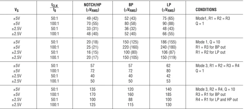
Table 2. Wideband RMS Noise
fCLK NOTCH/HP BP LP VS f0 (µVRMS) (µVRMS) (µVRMS) CONDITIONS ±5V 50:1 49 (42) 52 (43) 75 (65) Mode1, R1 = R2 = R3 ±5V 100:1 70 (55) 80 (58) 90 (88) Q = 1 ±2.5V 50:1 33 (31) 36 (32) 48 (43) ±2.5V 100:1 48 (40) 52 (40) 66 (55) ±5V 50:1 20 (18) 150 (125) 186 (155) Mode 1, Q = 10 ±5V 100:1 25 (21) 220 (160) 240 (180) R1 = R3 for BP out ±2.5V 50:1 16 (15) 100 (80) 106 (87) R1 = R2 for LP out ±2.5V 100.1 20 (17) 150 (105) 150 (119) ±5V 50:1 57 57 62 Mode 3, R1 = R2 = R3 = R4 ±5V 100:1 72 72 80 Q = 1 ±2.5V 50:1 40 40 42 ±2.5V 100.1 50 50 53 ±5V 50:1 135 120 140 Mode 3, R2 = R4, Q = 10 ±5V 100:1 170 160 185 R3 = R1 for BP out
±2.5V 50:1 100 88 100 R4 = R1 for LP and HP out
±2.5V 100:1 125 115 130
Short-Circuit Currents
Short circuits to ground, positive or negative power supply are allowed as long as the power supplies do not exceed
±5V and the ambient temperature stays below 85˚C.
Above ±5V and at elevated temperatures, continuous
short circuits to the negative power supply will cause excessive currents to flow. Under these conditions, the device will get damaged if the short-circuit current is allowed to exceed 80mA.
Each building block of the LTC1060, together with an external clock and a few resistors, closely approximates 2nd order filter functions. These are tabulated below in the frequency domain.
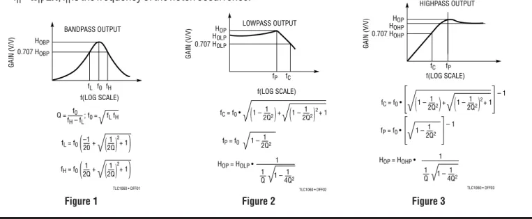
1.Bandpass function: available at the bandpass output Pins 2 (19). (Figure 1.)
G(s) = HOBP sωo/Q
s2 + (sωo/Q) + ωo2
HOBP = Gain at ω = ωo
f0 = ω/2π; f0 is the center frequency of the complex
pole pair. At this frequency, the phase shift between input and output is –180˚.
Q = Quality factor of the complex pole pair. It is the
ratio of f0 to the –3dB bandwidth of the 2nd
or-der bandpass function. The Q is always mea-sured at the filter BP output.
2.Lowpass function: available at the LP output Pins 1 (20). (Figure 2.) G(s) = HOLP ωo s2 + s(ωo/Q) + ω o 2 2
HOLP DC gain of the LP output.
APPLICATIO S I FOR ATIO
U
U
W
U
10
1060fb
3.Highpass function: available only in mode 3 at the ouput Pins 3 (18). (Figure 3.)
G(s) = HOHP
HOHP = gain of the HP output for f→
s2 s2 + s(ω o/Q) + ωo fCLK 2 2
4.Notch function: available at Pins 3 (18) for several modes of operation.
G(s) = (HON2)
HON2 = gain of the notch output for f→
s2 + ω2 o s2 + (sωo/Q) + ωo fCLK 2 2
HON1 = gain of the notch output for f→0
fn = ωn/2π; fn is the frequency of the notch occurrence.
5.Allpass function: available at Pins 3(18) for mode 4, 4a.
G(s) = HOAP
HOAP = gain of the allpass output for 0 < f <
[s2 – s(ω o/Q) + ωo] s2 + s(ωo/Q) + ω o fCLK 2 2 2
For allpass functions, the center frequency and the Q of the numerator complex zero pair is the same as the denominator. Under these conditions, the magnitude response is a straight line. In mode 5, the center frequency
fz, of the numerator complex zero pair, is different than f0.
For high numerator Q’s, the magnitude response will have a notch at fz.
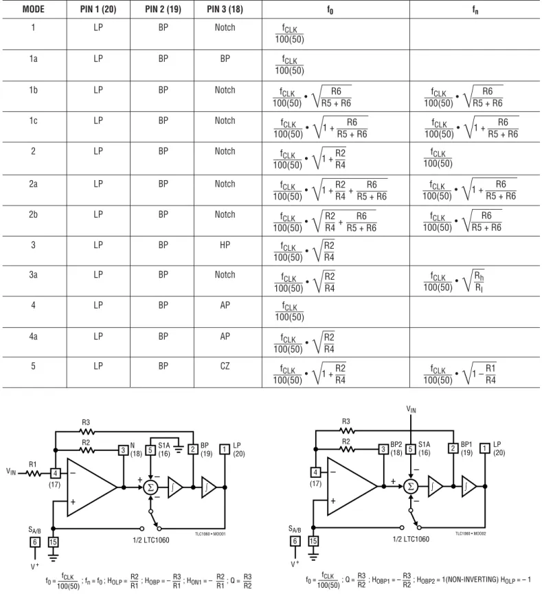
Table 3. Modes of Operation: 1st Order Functions
MODE PIN 2 (19) PIN 3 (18) fC fZ
6a LP HP • fCLK 100(50) R2 R3 6b LP LP • fCLK 100(50) R2 R3 7 LP AP • fCLK 100(50) R2 R3 • fCLK 100(50) R2 R3
Figure 1 Figure 2 Figure 3
f0 ; f 0 = fH –fL fL fH HOBP 0.707 HOBP f0 fL fH Q = –1 20 1 2 2Q fL = f0
(
+( (
+ 1)
1 2Q 1 2 2Q fH = f0(
+( (
+ 1)
BANDPASS OUTPUT f(LOG SCALE) GAIN (V/V) TLC1060 • DFF01 HOP HOLP fP fC 0.707 HOLP 1 2 2Q fC = f0 •(
1 – +(
1 + 1 2 2 2Q 1 –(
(
LOWPASS OUTPUT f(LOG SCALE) GAIN (V/V) TLC1060 • DFF02 1 2 2Q 1 1 Q fP = f0 HOP = HOLP • 1 – 1 2 4Q 1 – fC 1 2 2Q fC = f0 • 1 – + + 1 – 1 – 1 1(
(
1 2 2 2Q 1 –(
(
f(LOG SCALE) TLC1060 • DFF03 HOP HOHP fP 0.707 HOHP HIGHPASS OUTPUT GAIN (V/V) 1 2 2Q 1 Q fP = f0 • HOP = HOHP • 1 – 1 2 4Q 1 –DEFI
N
ITIO
U
N
U
OF FILTER FU
N
CTIO
U
N
S
U
11
1060fb
Table 4. Modes of Operation: 2nd Order Functions
MODE PIN 1 (20) PIN 2 (19) PIN 3 (18) f0 fn
1 LP BP Notch fCLK 100(50) 1a LP BP BP fCLK 100(50) 1b LP BP Notch 1c LP BP Notch 2 LP BP Notch fCLK 100(50) 2a LP BP Notch 2b LP BP Notch 3 LP BP HP 3a LP BP Notch 4 LP BP AP fCLK 100(50) 4a LP BP AP 5 LP BP CZ
Figure 4. Mode 1: 2nd Order Filter Providing Notch, Bandpass, Lowpass
Figure 5. Mode 1a: 2nd Order Filter Providing Bandpass, Lowpass
1/2 LTC1060 SA/B
VIN
f0 = fCLK ; fn = f0 ; HOLP = ; HOBP = – ; HON1 = – ; Q =
100(50) TLC1060 • MOO01 1 – + – – + R1 R3 R2 N (18) LP (20) BP (19) S1A (16) V + (17) R2 R1 R3 R1 R3 R2 R2 R1 15 4 3 5 2 Σ 6 ∫ ∫ 1/2 LTC1060 SA/B VIN
f0 = ; Q= ; HOBP1 = – ; HOBP2 = 1(NON-INVERTING) HOLP = – 1
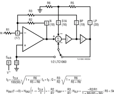
fCLK 100(50) TLC1060 • MOO02 1 – + – – + R3 R2 BP2 (18) LP (20) BP1 (19) S1A (16) V + (17) R3 R2 R3 R2 15 4 3 5 2 Σ 6 ∫ ∫ • fCLK 100(50) R6 R5 + R6 • fCLK 100(50) R6 R5 + R6 • 1 + fCLK 100(50) R6 R5 + R6 • 1 + fCLK 100(50) R6 R5 + R6 • 1 + fCLK 100(50) R2 R4 • 1 + fCLK 100(50) R6 R5 + R6 • 1 + + fCLK 100(50) R2 R4 R6 R5 + R6 • + fCLK 100(50) R2 R4 R6 R5 + R6 • fCLK 100(50) R6 R5 + R6 • fCLK 100(50) R2 R4 • fCLK 100(50) R2 R4 • fCLK 100(50) Rh RI • fCLK 100(50) R2 R4 • 1 + fCLK 100(50) R2 R4 • 1 – fCLK 100(50) R1 R4
ODES OF OPERATIO
W
U
12
1060fb
Figure 6. Mode 1b: 2nd Order Filter Providing Notch, Bandpass, Lowpass
Figure 7. Mode 1c: 2nd Order Filter Providing Notch, Bandpass, Lowpass
Figure 8. Mode 2: 2nd Order Filter Providing Notch, Bandpass, Lowpass
Figure 9. Mode 2a: 2nd Order Filter Providing Notch, Bandpass, Lowpass 1/2 LTC1060 SA/B VIN 1 + – – – + R3 R6 R5 R2 R1 N LP (20) BP (19) S1A (16) V – (17) 15 4 3 5 2 Σ 6 f0 = ; fn = f0 ; Q = fCLK 100(50) TLC1060 • MOO03 fCLK 2 R6 R5 + R6 R6 R5 + R6 R3 R2
(
)
–R2/R1 R6/(R5 + R6) R2 R1 H0N1(f 0)← = H0N2 f ← = – ; H0LP = ; H0BP = –R1R3; R5 < 5kΩ ∫ ∫ 1/2 LTC1060 SA/B VIN 1 + – – – + R3 R6 R5 R2 R1 N (18) LP (20) BP (19) S1A (16) V + (17) 15 4 3 5 2 Σ 6 f0 = 1 + ; fn = f0 ; Q = ; fCLK 100(50) TLC1060 • MOO04 fCLK 2 R6 R5 + R6 R3 R2(
)
1 + R6 R5 + R6 –R2/R1 1 + R6/(R5 + R6) R2 R1 H0N1(f 0)← = H0N2f ← = – ; H0BP = –R1R3; H0LP = ; R5 < 5kΩ ∫ ∫ 1/2 LTC1060 SA/B VIN 1 + – – – + R3 R4 R2 R1 N (18) LP (20) BP (19) S1A (16) V+ (17) 15 4 3 5 2 Σ 6 f0 = fCLK 1 + ; fn = ; Q = ; H0LP = 100(50) TLC1060 • MOO05 fCLK 100(50) fCLK 2 R3 R2 R2 R4(
)
1 +R2 R4 –R2/R1 1 + (R2 + R4) –R2/R1 1 + (R2 + R4) H0BP = – R3/R1 ; H0N1(f 0)← = ; H0N2 = f ← = – R2/R1 ∫ ∫ 1/2 LTC1060 SA/B VIN 1 + – – – + R3 R6 R5 R4 R2 R1 N (18) LP (20) BP (19) S1A (16) V+ (17) 15 4 3 5 2 Σ 6 f0 = 1 + + ; fn = ; Q = fCLK 100(50) TLC1060 • MOO06 fCLK 100(50) fCLK 2 R3 R2 R2 R1 R2 R4( )
R6 R5 + R6 1 + + R2 R4 R6 R5 + R6 1 + R6 R5 + R6 1 + R6/(R5 + R6) 1 + (R2/R4) + [R6/(R5 + R6)] –R2/R1 1 + (R2/R4) + [R6/(R5 + R6)] H0N1(f 0)← = – ; H0N2 f ← = – R2/R1 H0BP = – R3/R1 ; H0LP = ∫ ∫ODES OF OPERATIO
W
U
13
1060fb
Figure 10. Mode 2b: 2nd Order Filter Providing Notch, Bandpass, Lowpass
Figure 11. Mode 3: 2nd Order Filter Providing Highpass, Bandpass, Lowpass
Figure 12. Mode 3a: 2nd Order Filter Providing Highpass, Bandpass, Lowpass, Notch
1/2 LTC1060 SA/B VIN 1 + – – – + R3 R6 R5 R4 R2 R1 N (18) LP (20) BP (19) S1A (16) V – (17) 15 4 3 5 2 Σ 6 f0 = + ; fn = ; Q = fCLK 100(50) TLC1060 • MOO07 fCLK 100(50) fCLK 2 R3 R2 R2 R1 R2 R4
(
)
R6 R5 + R6 + R2 R4 R6 R5 + R6 R6 R5 + R6 R6/(R5 + R6) (R2/R4) + [R6/(R5 + R6)] –R2/R1 (R2/R4) + [R6/(R5 + R6)] H0N1(f 0)← = – ; H0N2 f ← = – R2/R1 H0BP = – R3/R1 ; H0LP = ∫ ∫ 1/2 LTC1060 SA/B VIN 1 + – – – + R3 R4 R2 R1 N (18) LP (20) BP (19) S1A (16) V – (17) 15 4 3 5 2 Σ 6 f0 = ; Q = ; H0HP = –R2/R1; H0BP = –R3/R1; H0LP = –R4/R1 fCLK 100(50) TLC1060 • MOO08 R3 R2 R2 R4 R2 R4 ∫ ∫ 1/2 LTC1060 NOTCH SA/B VIN 1 + – – – + R3 R4 R2 Rh Rg RI R1 HP (18) LP (20) BP (19) S1A (16) V – (17) 15 4 3 5 2 Σ 6 f0 = fCLK ; fn = ; H0HP = –R2/R1; H0BP = –R3/R1, H0LP = – R4/R1 100(50) TLC1060 • MOO09 fCLK 100(50) fCLK 2 R2 R4(
)
(
)
Rh RI Rg RI Rg RI Rg Rh R4 R1 R3 R2 R2 R4 H0N1(f 0)= • = Rg Rh R2 R1 • ; H0N2 f ; H0N(f = f0) = Q H0LP – H0HP ; Q = ← ← – + EXTERNAL OP AMP ∫ ∫ODES OF OPERATIO
W
U
14
1060fb
Figure 13. Mode 4: 2nd Order Filter Providing Allpass, Bandpass, Lowpass
Figure 14. Mode 4a: 2nd Order Filter Providing Highpass, Bandpass, Lowpass, Allpass
Figure 15. Mode 5: 2nd Order Filter Providing Numerator Complex Zeros, Bandpass, Lowpass
Figure 16. Mode 6a: 1st Order Filter Providing Highpass, Lowpass
1/2 LTC1060 SA/B
VIN
f0 = fCLK ; Q= ; HOAP = – ; HOLP = –2 HOBP = – 2
100(50) TLC1060 • MOO10 1 – + – – + R3 R2 R1 = R2 AP2 (18) LP (20) BP (19) S1A (16) V + (17) R3 R2 R3 R2 R2 R1 15 3 5 2 Σ 6 4
( )
∫ ∫ 1/2 LTC1060 SA/B VIN 1 + – – – + R3 R4 R2 2R R R5 R1 HP (18) LP (20) BP (19) S1A (16) V – (17) 15 4 5 2 Σ 6 f0 = ; Q= ; H0AP = ; H0HP = – ; H0BP = – fCLK 100(50) TLC1060 • MOO11 R2 R4 R3 R2 R3 R1; H0LP = – R4 R1 R2 R1 R5 2R R2 R4 – + EXTERNAL OP AMP 3 ∫ ∫ 1/2 LTC1060 SA/B VIN TLC1060 • MOO12 1 – + – – + R3 R4 R2 R1 CZ (18) LP (20) BP (19) S1A (16) V + (17) 15 3 5 2 Σ 6 4 f0 = Q2 = 1 + ; fz = ; Q = fCLK 100(50) fCLK 100(50) fCLK 2 R2 R4 R3 R1(
)
1 +R2 R4 1 –R1 R4 R3 R2 = 1 –R1R4; HOZ = (f 0)= R3 R2 =R2 R1 (R4/R1) –1 (R4/R2) + 1; HOZ f ; ← ←( )
R2 = R1 1 + (R2/R1) 1 + (R2/R4) HOBP 1 + ; HOLP ∫ ∫ 1/2 LTC1060 SA/B VIN 1 + – – – + R3 R2 R1 N (18) LP (20) BP (19) S1A (16) V – (17) 15 4 3 5 2 Σ 6 fC = ; H0LP = –R3/R1 ; H0HP = –R2/R1 fCLK R2 100(50) R3 TLC1060 • MOO13 ∫ ∫ODES OF OPERATIO
W
U
15
1060fb
CO
MM
W
E TS O
W
U
N
U
THE
M
ODES OF OPERATIO
W
U
There are basically three modes of operation: mode 1, mode 2, mode 3. In the mode 1 (Figure 4), the input amplifier is outside the resonant loop. Because of this, mode 1 and its derivatives (mode 1a, 1b, 1c) are faster than modes 2 and 3. In mode 1, for instance, the Q errors are becoming noticeable above 1MHz clock frequency. Mode 1a (Figure 5), represents the most simple hook-up of the LTC1060. Mode 1a is useful when voltage gain at the bandpass output is required. The bandpass voltage gain, however, is equal to the value of Q; if this is acceptable, a second order, clock tunable, BP resonator can be achiev-ed with only 2 resistors. The filter center frequency directly depends on the external clock frequency. For high order filters, mode 1a is not practical since it may require several clock frequencies to tune the overall filter response. Mode 1 (Figure 4), provides a clock tunable notch; the depth is shown in Graph 14. Mode 1 is a practical configuration for second order clock tunable bandpass/ notch filters. In mode 1, a bandpass output with a very high Q, together with unity gain, can be obtained without creating problems with the dynamics of the remaining notch and lowpass outputs.
Modes 1b and 1c (Figures 6 and 7), are similar. They both produce a notch with a frequency which is always equal to the filter building block center frequency. The notch and the center frequency, however, can be adjusted with an external resistor ratio.
The practical clock-to-center frequency ratio range is:
≥fCLK≥ f0 500 1 100 1 or ; mode 1b 50 1 ≥fCLK≥ fo 100 1 100 √2 or50 or ; mode 1c 1 50 √2
The input impedance of the S1 pin is clock dependent, and in general R5 should not be larger than 5k. Mode 1b can be used to increase the clock-to-center frequency ratio beyond 100:1. For this mode, a practical limit for the
(fCLK/f0) ratio is 500:1. Beyond this, the filter will exhibit
large output offsets. Mode 1c is the fastest mode of
operation: In the 50:1 mode and with (R5 = 0, R6 = ∞) the
clock-to-center frequency ratio becomes (50/√2) and
cen-ter frequencies beyond 20kHz can easily be achieved as shown in Graph 25. Figure 19 illustrates how to cascade the two sections of the LTC1060 connected in mode 1c to obtain a sharp fourth order, 1dB ripple, BP Chebyshev filter. Note that the center frequency to the BW ratio for this fourth order bandpass filter is 20/1. By varying the clock frequency to sweep the filter, the center frequency of the overall filter will increase proportionally and so will the BW to maintain the 20:1 ratio constant. All the modes of operation yield constant Q’s; with any filter realization the BW’s will vary when the filter is swept. This is shown in Figure 19, where the BP filter is swept from 1kHz to 20kHz center frequency.
Figure 17. Mode 6b: 1st Order Filter Providing Lowpass Figure 18. Mode 7: 1st Order Filter Providing Allpass, Lowpass
1/2 LTC1060 SA/B VIN fC = fCLK R2 ; HOLP1 = 1 ; HOLP2 = – 100(50) R3 TLC1060 • MOO14 1 – + – – + R3 R2 LP1 (18) (20) LP2 (19) S1A (16) V – (17) R3 R2 15 4 3 5 2 Σ 6 ∫ ∫ 1/2 LTC1060 SA/B VIN
fP = ; fz = ; GAIN AT AP OUTPUT = 1 FOR 0 ≤ f ≤
HOLP = 2 x fCLK R2 100(50) R3 TLC1060 • MOO15 1 – + – – + R3 R2=R1 R1=R2 AP (18) (20) LP (19) S1A (16) V – (17) fCLK R2 100(50) R3 fCLK 2 R3 R2 15 3 5 2 Σ 6 4 ∫ ∫
ODES OF OPERATIO
W
U
16
1060fb
Modes 2, 2a, and 2b have a notch output which frequency,
fn, can be tuned independently from the center frequency,
f0. For all cases, however, fn<f0. These modes are useful
when cascading second order functions to create an
overall elliptic highpass, bandpass or notch response. The input amplifier and its feedback resistors (R2/R4) are now part of the resonant loop. Because of this, mode 2 and its derivatives are slower than mode 1’s.
In mode 3 (Figure 11), a single resistor ratio (R2/R4) can
tune the center frequency below or above the fCLK/100
(or fCLK/50) ratio. Mode 3 is a state variable configuration
since it provides a highpass, bandpass, lowpass output through progressive integration; notches are obtained by summing the highpass and lowpass outputs (mode 3a, Figure 12). The notch frequency can be tuned below or above the center frequency through the resistor ratio
(Rh/Ri). Because of this, modes 3 and 3a are the most
versatile and useful modes for cascading second order sections to obtain high order elliptic filters. Figure 20 shows the two sections of an LTC1060 connected in mode 3a to obtain a clock tunable 4th order sharp elliptic bandpass filter. The first notch is created by summing directly the HP and LP outputs of the first section into the inverting input of the second section op amp. The indi-vidual Q’s are 29.6 and the filter maintains its shape and performance up to 20kHz center frequency (Figure 21). For this circuit an external op amp is required to obtain the 2nd notch. The dynamics of Figure 20 are excellent
be-cause the amplitude response at each output pin does not exceed 0dB. The gain in the passband depends on the ratio
of (Rg/Rh2) • (R22/Rh1)• (R21/R11). Any gain value can be
obtained by acting on the (Rg/Rh2) ratio of the external op
amp, meanwhile the remaining ratios are adjusted for optimum dynamics of the LTC1060 output nodes. The external op amp of Figure 20 is not always required. In Figure 22, one section of the LTC1060 in mode 3a is cascaded with the other section in mode 2b to obtain a 4th order, 1dB ripple, elliptic bandreject filter. This configura-tion is interesting because a 4th order funcconfigura-tion with two different notches is realized without requiring an external op amp. The clock-to-center frequency ratio is adjusted to 200:1; this is done in order to better approximate a linear R,C notch filter. The amplitude response of the filter is shown in Figure 23 with up to 1MHz clock frequency. The 0dB bandwidth to the stop bandwidth ratio is 9/1. When the filter is centered at 1kHz, it should theoretically have a 44dB rejection with a 50Hz stop bandwidth. For a more narrow filter than the above, the unused BP output of the
Figure 19. Cascading the Two Sections of the LTC1060 Connected in Mode 1c to Obtain a Clock Tunable 4th Order 1dB Ripple Bandpass Chebyshev Filter with (Center Frequency)/(Ripple Bw) = 20/1.
0.9kHz –15dB –10dB –5dB 0dB 1.1kHz –25dB –20dB 1kHz 50Hz fCLK = 40kHz 18kHz –15dB –10dB –5dB 0dB 22kHz TLC1060 • CMO01b –25dB –20dB 20kHz 19kHz 21kHz 1kHz fCLK = 800kHz LTC1060 • CM01 VIN R31 R21 R52 R32 1 2 3 4 5 6 7 8 9 10 20 19 18 17 16 15 14 13 12 11 V+ = 5V VOUT T2L OR CMOS CLK IN R51 R22 R62 R12 LPA BPA NA INVA S1A SA/B VA+ VD+ LSh CLKA LPB BPB NB INVB S1B AGND VA– VD– 50/100 CLKB LTC1060 R61 R11 5V
PRECISE RESISTOR VALUES R11 = 149.21k R21 = 4.99k R31 = 149.12k R51 = 2.55k R61 = 2.49k R12 = 45.14k R22 = 5.00k R32 = 142.64k R5 = 2.49k R62 = 4.29k V– = –5V
17
1060fb
mode 2b section (Figure 22), has a gain exceeding unity which limits the dynamic range of the overall filter. For very selective bandpass/bandreject filters, the mode 3a
approach, as in Figure 20, yields better dynamic range since the external op amp helps to optimize the dynamics of the output nodes of the LTC1060.
Figure 20. Combining Mode 3 with Mode 3a to Make The 4th Order BP Filter of Figure 21 with Improved
Dynamics. The Gain at Each Output Node is ≤ 0dB for all Input Frequencies.
Figure 21. The BP Filter of Figure 20, When Swept From a 2kHz to 20kHz Center Frequency.
1.5kHz –30dB –20dB –10dB 0dB 2.5kHz –50dB –40dB 2kHz 1.75kHz 2.25kHz fCLK = 100kHz 15kHz –30dB –20dB –10dB 0dB 25kHz –50dB –40dB 20kHz 17.5kHz 22.5kHz fCLK = 1MHz TLC1060 • CMO03 LTC1060 • CM02 VIN R42 R32 1 2 3 4 5 6 7 8 9 10 20 19 18 17 16 15 14 13 12 11 V+ = 7.5V –7.5V VOUT T2L OR CMOS CLOCK IN R22 LTC1060 R11 7.5V
PRECISE RESISTOR VALUES R11 = 155.93k
RH1 = 13.2k
R42 = 5k
NOTE: FOR CLOCK FREQUENCIES ABOVE 700kHz, A 12pF CAPACITOR ACROSS R41 AND A 20pF CAPACITOR ACROSS R42 WERE USED TO PREVENT THE PASSBAND RIPPLE FROM ANY ADDITIONAL PEAKING R21 = 5k RL1 = 10.74k RL2 = 6.11k R31 = 152k R22 = 5.26k RH2 = 5k R41 = 5.27k R32 = 151.8k RG = 37.3k –7.5V R31 R21 R41 RL1 RH1 RL2 RH2 – + RG EXTERNAL OP AMP LPA BPA HPA INVA S1A SA/B VA+ VD+ LSh CLKA LPB BPB HPB INVB S1B AGND VA– VD– 50/100 CLKB
18
1060fb
Figure 22. Combining Mode 3 with Mode 2b to Create a 4th Order BR Elliptic Filter with 1dB Ripple and a Ratio of 0dB to Stop Bandwidth Equal to 9/1.
Figure 23. Amplitude Response of the Notch Filter of Figure 22
Switched capacitor integrators generally exhibit higher input offsets than discrete R, C integrators. These offsets are mainly due to the charge injection of the CMOS switches into the integrating capacitors and they are temperature independent.
The internal op amp offsets also add to the overall offset budget and they are typically a couple of millivolts. Be-cause of this, the DC output offsets of switched capacitor filters are usually higher than the offsets of discrete active filters.
Figure 24 shows half of an LTC1060 filter building block
with its equivalent input offsets VOS1, VOS2, VOS3. All three
are 100% tested for both sides of the LTC1060. VOS2 is
generally the larger offset. When the SA/B, Pin 6, of the
LTC1060 is shorted to the negative supply (i.e., mode 3),
the value of the VOS2 decreases. Additionally, with SA/B
low, a 20% to 30% noise reduction is observed. Mode 1 can still be achieved, if desired, by shorting the S1 pin to the lowpass output (Figure 25).
LTC1060 • CM04 VIN R31 R21 R52 R32 1 2 3 4 5 6 7 8 9 10 20 19 18 17 16 15 14 13 12 11 V+ = – 5V – 5V VOUT T2L OR CMOS CLOCK IN R41 RL1 RH1 R22 R62 R42 LPA BPA HPA INVA S1A SA/B VA+ VD+ LSh CLKA LPB BPB NB INVB S1B AGND VA– VD– 50/100 CLKB LTC1060 R11 RESISTOR VALUES R11 = 60k R41 = 28.84k R52 = 5k R32 = 455.75k R21 = 5k RH1 = 5k R62 = 1.59k R42 = 503.85k R31 = 54.75k RL1 = 19.3k R22 = 60k V– = – 5V 0.7 –30 –20 –10 0 1.1 1.2 1.3 – 60 – 50 – 40 0.9 0.8 f0 = 1.0 VOUT /VIN (dB)
INPUT FREQUENCY NORMALIZED TO FILTER CENTER FREQUENCY
TLC1060 • CMO05 fCLK f0 200 1 = ; fCLK ≤ 1MHz + (17) 4 + + – – – – – + (18) (16) (19) (20) 15 VOS1 VOS2 3 5 Σ TLC1060 • LO01 1 2 – + – + + – VOS3
Figure 24. Equivalent Input Offsets of 1/2 LTC1060 Filter Building Block
Figure 25. Mode 1(LN): Same Operation as Mode 1 but Lower
VOS2 Offset and Lower Noise
LTC1060 OFFSETS
CO
MM
W
E TS O
W
U
N
U
THE
M
ODES OF OPERATIO
W
U
1/2 LTC1060 SA/B VIN 1 + – – – + R3 R2 R1 N (18) LP (20) BP (19) S1A (16) V – (17) 15 4 3 5 2 Σ 6 TLC1060 • LO02 ∫ ∫
19
1060fb
Output Offsets
The DC offset at the filter bandpass output is always equal
to VOS3. The DC offsets at the remaining two outputs
(Notch and LP) depend on the mode of operation and external resistor ratios. Table 5 illustrates this.
It is important to know the value of the DC output offsets, especially when the filter handles input signals with large
dynamic range. As a rule of thumb, the output DC offsets increase when:
1. The Q’s decrease.
2. The ratio (fCLK/f0) increases beyond 100:1. This is
done by decreasing either the (R2/R4) or the R6/(R5 + R6) resistor ratios.
Information furnished by Linear Technology Corporation is believed to be accurate and reliable. However, no responsibility is assumed for its use. Linear Technology Corporation makes no represen-tation that the interconnection of its circuits as described herein will not infringe on existing patent rights.
N Package
20-Lead PDIP (Narrow .300 Inch)
(Reference LTC DWG # 05-08-1510)
LTC1060 OFFSETS
U
PACKAGE DESCRIPTIO
.255 ± .015* (6.477 ± 0.381) 1.040* (26.416) MAX 1 2 3 4 5 6 7 8 9 10 19 18 17 16 15 14 13 12 11 20 NOTE:1. DIMENSIONS ARE INCHES MILLIMETERS
*THESE DIMENSIONS DO NOT INCLUDE MOLD FLASH OR PROTRUSIONS. MOLD FLASH OR PROTRUSIONS SHALL NOT EXCEED .010 INCH (0.254mm)
N20 1002 .020 (0.508) MIN .120 (3.048) MIN .125 – .145 (3.175 – 3.683) .065 (1.651) TYP .045 – .065 (1.143 – 1.651) .018 ± .003 (0.457 ± 0.076) .005 (0.127) MIN .100 (2.54) BSC .008 – .015 (0.203 – 0.381) .300 – .325 (7.620 – 8.255) .325+.035–.015 +0.889 –0.381 8.255
(
)
Table 5VOSN VOSBP VOSLP
MODE PIN 3 (18) PIN 2 (19) PIN 1 (20)
1,4 VOS1 [(1/Q) + 1 + ||HOLP||] – VOS3/Q VOS3 VOSN – VOS2
1a VOS1 [1 + (1/Q)] – VOS3/Q VOS3 VOSN – VOS2
1b VOS1 [(1/Q) + 1 + R2/R1] – VOS3/Q VOS3 ~ (VOSN – VOS2) (1 + R5/R6)
1c VOS1 [(1/Q) + 1 + R2/R1] – VOS3/Q VOS3 (R5 + R6)
(R5 + 2R6)
~ (VOSN – VOS2)
2, 5 [VOS1(1 + R2/R1 + R2/R3 + R2/R4) – VOS3(R2/R3)] VOS3 VOSN – VOS2
• [R4/(R2 + R4)] + VOS2[R2/(R2 + R4)] 2a VOS3 (R5 + R6) (R5 + 2R6) ~ (VOSN – VOS2) 2b
VOS3 ~ (VOSN – VOS2) (1 + R5/R6)
3, 4a VOS2 VOS3 R4 R1 VOS1 1 + +R4R2+R4R3 – VOS2 R4R2 – VOS3 R4 R3 R4(1 + k) R2 + R4(1 + k) + VOS2 ;k = • R2 R2 + R4(1 + k) R6 R5 + R6 [VOS1(1 + R2/R1 + R2/R3 + R2/R4) – VOS3(R2/R3)] R4k R2 + R4k + VOS2 ;k = • R2 R2 + R4k R6 R5 + R6 [VOS1(1 + R2/R1 + R2/R3 + R2/R4) – VOS3(R2/R3)]
20
1060fb
Linear Technology Corporation
1630 McCarthy Blvd., Milpitas, CA 95035-7417 (408) 432-1900 ● FAX: (408) 434-0507 ● www.linear.com
LW/TP 1202 1K REV B • PRINTED IN USA
LINEAR TECHNOLOGY CORPORATION 1988
J Package
20-Lead CERDIP (Narrow .300 Inch, Hermetic)
(Reference LTC DWG # 05-08-1110)
OBSOLETE PACKAGE
S20 (WIDE) 0502 NOTE 3 .496 – .512 (12.598 – 13.005) NOTE 4 20 N 19 18 17 16 15 14 13 1 2 3 4 5 6 7 8 .394 – .419 (10.007 – 10.643) 9 10 N/2 11 12 .037 – .045 (0.940 – 1.143) .004 – .012 (0.102 – 0.305) .093 – .104 (2.362 – 2.642) .050 (1.270) BSC .014 – .019 (0.356 – 0.482) TYP 0° – 8° TYP NOTE 3 .009 – .013 (0.229 – 0.330) .016 – .050 (0.406 – 1.270) .291 – .299 (7.391 – 7.595) NOTE 4 × 45° .010 – .029 (0.254 – 0.737) .420 MIN .325 ±.005RECOMMENDED SOLDER PAD LAYOUT .045 ±.005 N 1 2 3 N/2 .050 BSC .030 ±.005 TYP .005 (0.127) RAD MIN INCHES (MILLIMETERS) NOTE: 1. DIMENSIONS IN 2. DRAWING NOT TO SCALE
3. PIN 1 IDENT, NOTCH ON TOP AND CAVITIES ON THE BOTTOM OF PACKAGES ARE THE MANUFACTURING OPTIONS. THE PART MAY BE SUPPLIED WITH OR WITHOUT ANY OF THE OPTIONS
4. THESE DIMENSIONS DO NOT INCLUDE MOLD FLASH OR PROTRUSIONS. MOLD FLASH OR PROTRUSIONS SHALL NOT EXCEED .006" (0.15mm)
SW Package
20-Lead Plastic Small Outline (Wide .300 Inch)
(Reference LTC DWG # 05-08-1620)
U
PACKAGE DESCRIPTIO
J20 0801 3 5 6 7 9 10 1 2 4 8 11 20 19 18 17 16 15 14 13 12 .005 (0.127) MIN .025 (0.635) RAD TYP .220 – .310 (5.588 – 7.874) 1.060 (26.924) MAX 0° – 15° .008 – .018 (0.203 – 0.457) .015 – .060 (0.381 – 1.524) .125 (3.175) MIN .014 – .026 (0.356 – 0.660) .045 – .065 (1.143 – 1.651) (2.54).100 BSC .200 (5.080) MAX .300 BSC (7.62 BSC) .045 – .065 (1.143 – 1.650) FULL LEAD OPTION .023 – .045 (0.584 – 1.143) HALF LEAD OPTION CORNER LEADS OPTION(4 PLCS)
NOTE: LEAD DIMENSIONS APPLY TO SOLDER DIP/PLATE OR TIN PLATE LEADS