Impact of image features on the electron microscope sweep circuits
Meizhi Zhang
Inner Mongolia Electronic Information College Hohhot, Inner Mongolia, 010050, China. [email protected]
ABSTRACT: This study deduced a set of theory computational formula, and optimized and improved the heat-conductivity of vias in printed circuit board (PCB) of electrical power apparatus. We adopted numerical simulation and experimental measurement to verify the reliability of this formula. Through the theory computational formula, this paper studied the influence of aperture of vias, filled materials and thickness of copper plated on vias on thermal conductivity. Research result showed that 0.45mm was the optimal diameter of bore of vias; the conductivity had no obvious improvement when filling material was FR4 or Rogers, but if it was filled with texture of high thermal conductivity like soldering tine, the conductivity would improved a lot; the plating thickness of vias had greater influence on thermal conductivity. The adoption of three optimization scheme of vias recommended by the result could respectively improve 6.5%, 35% and 51% of thermal conductivity.
Keywords: Heat dissipation vias, Thermal conductivity, Copper plating thickness, Thermal simulation
Received: 11 August 2016, Revised 10 September 2016, Accepted 18 September 2016
© 2016 DLINE. All Rights Reserved 1. Introduction
its working mode, collects information and acquires microscopic appearance characteristics and chemical composition information of the material using different information detector according to the mechanism of different information when high-energy electron interacts with substances. EM is able to allocate different detector components with a variety of functions to meet the specific application requirements (Tu, 2012), and the continuous development of SEM technology has become an indispensable tool in scientific research institutions and enterprises for high-tech research and routine analytical test (Zhang, 2012).
The greatest strength of SEM is to change the temperature, gas composition and pressure in microscope sample room, which solves the limitation of high vacuum in sample room from conventional SEM and non-conducting material is capable of scanning (Yu, 2000). Sweep circuit, the heart of SEM, directly affects the imaging quality and output image resolution of SEM. EM, divided into SEM and transmission electron microscope (TEM), is mainly made up of electronic gun, image capture, display system and vacuum system. The image resolution and definition of EM is influenced by the size of electron beam spot, stability of acceleration voltage, aberration and astigmatism of magnetic lens in electron optical system, electronic noise of image acquisition, vibration of mechanical parts, noise of scanning signal and irregular deflection of electron beam caused by nonlinearity, etc (Sandra and Dirk, 2006).
2. Computer image acquisition
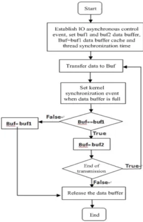
Computer image acquisition and display are completed by computer USB communication program and data processor. Data processor is used for processing image data and displaying image data after processing on computer screen; USB communication program includes USB driver and USB application program, the former controls equipment by invoking device driver to concentrate the USB communication program writing on image data transmission, and the latter mainly contains USB device initialize and data transmission. Sweep signal has an important influence on EM imaging quality, and it is hard to acquire high quality images. Main reasons influencing EM imaging quality include accelerated voltage, sweep speed and signal to noise ratio (SNR), beam spot diameter and working distance, probe electric current, astigmatism calibration (Zhang, 2004; Zhou, 2010; Tang and Qu, 2005; Liu et al., 2003). Figure 1 shows the process of USB data transmission.
3. Development of sweep circuit
The main function of sweep circuit is to output frame and line scanning signals, drive deflected scanning coil to control the deflection of electron beam, output and scan synchronizing signal, and synchronize image acquisition and display. Sweep circuit has two ways to produce sweep signal: one of them is to produce linear scanning signal using capacitance charge-discharge of analog circuit. According to the capacitance characteristic equations and in circuit theory can be obtained, in which, changes linearly with time, and linear sweep voltage signal is acquired. The other one is to generate linear voltage signal through high-speed digital analog converter (DAC), which is flexible in control and simple in design.
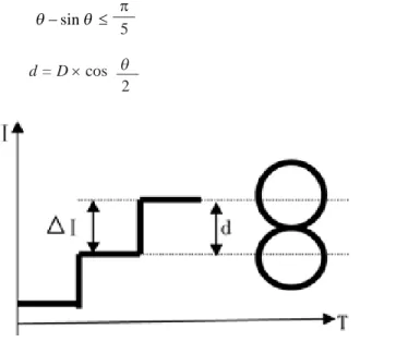
The image resolution of EM is decided by various factors. Assume the electron beam spot is a round with the diameter of D, and the electric current changes in corresponding scanning coil when electron beam is tangent with scanning adjacent two points on the surface of sample is ΔI (figure 2), the distance between two spots center is d = D at this time. The noise in electric circuit will change current in scanning coil, thus making two adjacent beam spots overlap. Assume Äi is the current change induced by noise. Generally speaking, two beam spots can be distinguished when the overlapping area of two adjacent beam spots is 20% smaller than electron beam spot area (figure 3), and the shaded area is 20% larger than area of the round. A geometrical relationship can be obtained based on above.
π θ − sinθ ≤
5 (1)
d = D × cos θ
2 (2)
Figure 2. Location relationships between scanning signal and scanning electron beam spot
In formula (1), θ ≤ 1.626 (radian) is obtained using numerical value, i.e., θ ≤ 93.20; if substituting è into formula (2), d ≥ 0.69D is available. Two adjacent electron beam spots is believed to be separated completely as long as the actual moving distance d of scanning spot is 0.69 time larger than diameter of electron beam spot. The distance of two adjacent scanning spots is linearly related to current change ΔI in coil, so two adjacent scanning spots is identified as parted as long as current change caused by noise in scanning coil is Δi ≤ 0.31 ΔI.
Sweep circuit is made up of three modules of control module, sweep signal production module, signal amplification module. Control module, including C8051F120 single chip microcomputer and its necessary external circuit for work, works normally when direct current 3.3 v working voltage and corresponding decoupling capacitance, JATG program debugging interface, clock vibration source, RS232 serial interface circuit are ready. The core of sweep signal production module is high-speed DAC, one of them is used for generating line scanning signal, and the other one is applied to producing frame scanning signal. The process of control program is displayed in figure 4.
4. Control of SEM scanning circuit based on computer image acquisition
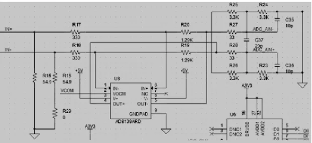
There are three difficulties in the design of computer image acquisition circuit: first is to ensure distortionless image signal input in the process of analog to digital converter (ADC); second is to transfer image data to computer in time; third is to synchronize image data and electron beam deflection. Two points, suitable bandwidth of signal amplification circuit in the front end of DAC, matched DAC input interface and front-end amplifying circuit impedance, are critical in order to guarantee distortionless image signal input in the process of DAC. Image signal is required to be amplified appropriately before it is converted into digital signal because the signal output by signal detector of electron microscope is weak. Image data conversion mainly converts amplified image signal into image data with AD9245, then it is saved into FIFO buffer. AD9245 front-end amplifier amplifies image signal using AD8139 differential operational amplifier, and part of the principle of signal amplification is shown in figure 5.
EM changes the angle of deflection of electron beam through altering the magnetic field produced by scanning coil, thereby obtaining its scanned image after electron beam scans the surface of sample. Electron beam has to scan the surface of sample evenly; otherwise, the obtained image will be distorted, so the magnetic field produced by scanning coil has to change linearly
Figure 5. Part of the principle of signal amplification
and evenly. Thus, the current through scanning coil also changes on average. Figure 6 explains the principle of sweep current signal production, and the whole sweep circuit consists of three parts: micro control unit (MCU), digital/analog converter and current amplification.
Figure 6. Principle of sweep current signal production
MCU is able to control high-speed DAC output to produce sweep signal, and meanwhile control current amplification module to amplify sweep signal produced by high-speed DAC to required range and load it into scanning field produced by scanning coil to realize electronic scanning. The core of DAC is high speed, high precision and low noise, which aims to convert accurate digital scanning signal into analog current signal. Different DAC has diverse output analog signal linearity, and sectional convertor had good monotonicity less differential linearity errors (Wang, 2011; Si and He, 2011; Li, 2011), hence, it has excellent linearity output.
5. Conclusion
Computer image acquisition controls the scanning circuit of SEM, and SEM hand image data processing over computer, which greatly reduce the complexity of image acquisition circuit and computer can process image data in a high speed. Image acquisition circuit applying USB for transferring image data not only make sure distortionless in the process of image data transmission, but also processes and displays image data timely, improving the scanning speed of EM consequently. Larger noise of sweep signal, undesirable interface of analog image signal of image acquisition circuit and image signal reflection observed in debugging process reduce dynamic range of analog digital conversion of acquisition circuit, which are issues existing in this study and need further improvement.
References
[2] Jon, O. (2009). Handbook of Charged Particle Optics Second Edition. New York: Taylor & Francis Group.
[3] Liu, YS., Liu, Y, Huang, L., Zeng, JG. (2014). Application and Development Trend of Microscope in the Experiment Teaching and Scientific Research. Theory and Practice of Contemporary Education. 6 (10) 66-69.
[4] Li, P, (2011). DAC Design of 12 Bit 80 MHZ Current Steering. Xi’an Electronic and Eng. Univ.
[5] Liu, JS., Xie, F., Wu, XJ., Chen, Y, Hu, G. (2003). Scanning Electron Microscope. Shanghai Measurement and Testing 30 (6) 37-39
[6] Sandra, V A., Dirk, V.D. (2006). Resolution of Coherent and Incoherent Imaging Systems Reconsidered-classical Criteria and a Statistical Alternative. Optics Express 14 (9) 3830-3839.
[7] Si, H.W, He, L.N. (2011).Analysis and Modeling of Dynamic Error in Current-steering DAC. Mechanical & Electrical Eng. Magazine. 28 (7) 850-854.
[8] Wang, Y. (2011). System Modeling and Validation of High Speed D/A Converter. Xi’an Electronic and Eng. Univ.
[9] Tang, X.S, Qu JL, (2005).Defeds and Improvesent of Images from Scanning Electronic Microscope, J. of Zhanjiang Normal College. 26 (3) 123-125
[10] Tu, J.J. (2012). Scanning Circuit and Image Acquisition Circuit of Scanning Electron Microscope. Shanghai Normal Univ.
[11] Yu, S.Y. (2000). The Characteristics and Development of Conventional Scanning Electron Microscope. Analytical Instrumentation (1) 51-53.
[12] Zhang, Z.K. (2012). Noise Control of Main Control System of Scanning Electron Microscopy. Nanjing Univ.