Doc. NO: QRD-310
DMZ1015E/DMX1015E
Full Datasheet
Issue of Department: RD
According to GB/T19001-2016 idt ISO9001:2015
Prepared by
:
Review by
:
Countersign by
:
Approved by
:
Effective Date
:
2020/12/24
Rev. Description of Change(s) ECN No. Eff. Date Prepared by
1.0 Initialization -- 2019/09/03 Zhongjian Zhou
2.0 Zhongjian Zhou
2.1 Change the test method of ESD 2020/05/29 Chuan Zhong
2.2 Update Package Dimensions 2020/10/12 Zhongjian Zhou
Ultrahigh Threshold Voltage Depletion-Mode Power MOSFET
General Features
ESD Improved Capability
Depletion Mode (Normally On)
Proprietary Advanced Planar Technology
Proprietary Advanced Ultrahigh Vth Technology
RoHS Compliant
Halogen-free Available
Applications
Quick Charger
Current Source
Voltage Source
General Description
This novel depletion mode MOSFET, developed and manufactured by ARK proprietary ultrahigh threshold voltage technology. By using the sub threshold characteristics, the depletion mode MOSFET can provide stably power to the load, and the voltage can be clamped to protect the load without Zener diode, and the circuit consumption is reduced.
Ordering Information
Part Number
Package
Marking
Remark
DMZ1015E SOT-23 1015 Halogen Free
DMX1015E SOT-89 1015 Halogen Free
Absolute Maximum Ratings
TA=25℃ unless otherwise specifiedSymbol Parameter DMZ1015E DMX1015E Unit
VDSX Drain-to-Source Voltage [1]
100 V
ID Continuous Drain Current 0.1
A IDM Pulsed Drain Current
[2]
0.4
PD Power Dissipation 0.5 1.0 W
VGS Gate-to-Source Voltage ±30 V
VESD
Gate to Source ESD[3] 700 V
Source to Gate ESD[3] 700 V
TL
Soldering Temperature
Distance of 1.6mm from case for 10 seconds 300 ℃
TJ and TSTG Operating and Storage Temperature Range -55 to 150
Caution: Stresses greater than those listed in the “Absolute Maximum Ratings” may cause permanent damage to the device.
Thermal Characteristics
Symbol Parameter DMZ1015E DMX1015E Unit
RθJA Thermal Resistance, Junction-to-Ambient 250 125 K/W
D G S SOT-23 D S G D D S G SOT-89
Electrical Characteristics
OFF Characteristics
TA =25℃ unless otherwise specified
Symbol Parameter Min. Typ. Max. Unit Test Conditions
BVDSX Drain-to-Source Breakdown Voltage 100 -- -- V VGS=-30V, ID=1mA
IGSS Gate-to-Source Leakage Current
-- -- 20
µA
VGS=+30V, VDS=0V
-- -- -20 VGS=-30V, VDS=0V
ON Characteristics
TA =25℃ unless otherwise specified
Symbol Parameter Min. Typ. Max. Unit Test Conditions
IDSS Saturated Drain-to-Source Current 100 -- -- mA VGS=0V, VDS=25V
RDS(ON) Static Drain-to-Source On-Resistance -- -- 30 Ω VGS=0V,ID=100mA [4]
VGS(OFF) Gate-to-Source Cut-off Voltage -- -- -27 V VDS=9V, ID=8µA
VCL Source-to-Gate Clamp Voltage 11.5 -- -- V VDS=9V, ID=5mA
Source-Drain Diode Characteristics
TA=25℃ unless otherwise specified
Symbol Parameter Min Typ. Max. Units Test Conditions
VSD Diode Forward Voltage -- -- 1.2 V ISD=100mA, VGS=-30V
NOTE:
[1] TJ=+25℃ to +150℃
[2] Repetitive rating, pulse width limited by maximum junction temperature. [3] The test is based on JEDEC EIA/JESD22-A114 (HBM).
Typical and highlight Characteristics
DMZ1015E/ DMX1015E is an ultra-high threshold voltage depletion mode MOS device. A stable output voltage source or current source is implemented by using the sub-threshold characteristics of the device. Its basic application is shown as Figure 1:
DMZ1015E/DMX1015E
RL
D S
G
Vin+
Vin
-Vout+
Vout
-Figure1. Drain Current ID is decided by Load Resistance
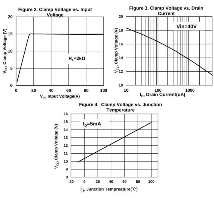
0 5 10 15 20
0 20 40 60 80 100
VCL , Cla m p Vol ta ge (V)
Vin, Input Voltage(V)
Figure 2. Clamp Voltage vs. Input Voltage
RL=2kΩ
10 12 14 16 18 20
10 100 1000
VCL , Cla m p Vol ta ge (V)
ID, Drain Current(uA)
Figure 3. Clamp Voltage vs. Drain Current Vin=40V 8 9 10 11 12 13 14 15 16
-20 0 20 40 60 80 100
VCL , Cla m p Vol ta ge (V)
TJ, Junction Tempreature(℃)
Figure 4. Clamp Voltage vs. Junction Temperature
Typical Application
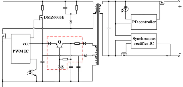
In the QC2.0/3.0 and Type-C/PD charger circuits, using DMZ1015E/DMX1015E as a high voltage linear regulagors can make the PWM IC power supply circuit more simplified, as shown below:
In Figure 5, the transistor Q is used to provide power, and the zener diode Z is used to clamp voltage, the power supply circuit of IC is composed of several components.
DMZ6005E
PWM IC
Q
Z
VCC
PD controller
Synchronous rectifier IC
+
-Figure 5. Normal Circuit with Transistor and Diode
In Figure 6, providing power and clamp voltage use only one device- DMZ1015E /DMX1015E, the circuit is simplified.
DMZ6005E
PWM IC
VCC
PD controller
Synchronous rectifier IC
+
-DMZ1015E /DMX1015E
Figure 6. Circuit with DMZ1015E/DMX1015E
At room temperature and under 2~4mA working current (most IC’s working current), the output voltage of DMZ1015E/DMX1015E is between 12~22V.
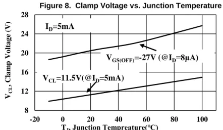
Due to strict design and process control,DMZ1015E/DMX1015E parameters have good consistency, but there are still some VGS(OFF) parameter distribution range, so we strictly control the final testing standard, the upper limit is ∣VGS(OFF)∣=27V (under normal temperature ID=8μA), the lower limit is VCL=11.5V of clamping voltage ( under
8μA≤ID≤5mA, the clamping voltage: 11.5V≤VCL≤27V. Figure 7 shows the clamping voltage VCL lower limit of
11.5V and the threshold voltage VGS(OFF) upper limit of VGS(OFF) =-27V, and the clamping working voltage
distribution when the working current does not exceed 5mA.
The clamping voltage will also change with the temperature. When the working temperature increases, the clamping voltage will increase; when the working temperature decreases, the clamping voltage will also decrease.
As shown in Figure 8, in the practical application of DMZ1015E/DMX1015E, with the increase of device temperature, its output voltage will also increase, and the drain-source voltage will decrease, so that the device's power consumption will also decrease. In this way, the temperature of DMZ1015E/DMX1015E will decrease. This negative feedback mechanism enables DMZ1015E/ DMX1015E to reach a stable thermal equilibrium state.
Ultra-high threshold voltage depletion mode MOSFET and its application were first proposed by ARK Microelectronics Co., LTD. Design engineers can determine the applicable range of DMZ1015E/DMX1015E according to the product specifications of DMZ1015E/DMX1015E and this application note.
10 14 18 22 26
10 100 1000
VCL , Cla m p Vo lt a g e (V)
ID, Drain Current(μA)
Figure 7. Clamp Voltage vs. Drain Current
Vin=40V
VGS(OFF)=-27V (@ID=8μA)
VCL=11.5V(@ID=5mA)
8 12 16 20 24 28
-20 0 20 40 60 80 100
VCL , Cla m p Vo lt a g e (V)
TJ, Junction Tempreature(℃)
Figure 8. Clamp Voltage vs. Junction Temperature
ID=5mA
VGS(OFF)=-27V (@ID=8μA) VCL=11.5V(@ID=5mA)
Published by
ARK Microelectronics Co., Ltd.
ADD: D26,UESTC National Science Park No. 1 Shuangxing Avenue, Chengdu, Sichuan.
All Rights Reserved.
Disclaimers
ARK Microelectronics Co., Ltd. reserves the right to make change without notice in order to improve reliability, function or design and to discontinue any product or service without notice. Customers should obtain the latest relevant information before orders and should verify that such information is current and complete. All products are sold subject to ARK Microelectronics Co., Ltd’s terms and conditions supplied at the time of order acknowledgement.
ARK Microelectronics Co., Ltd. warrants performance of its hardware products to the specifications at the time of sale, Testing, reliability and quality control are used to the extent ARK Microelectronics Co., Ltd deems necessary to support this warrantee. Except where agreed upon by contractual agreement, testing of all parameters of each product is not necessary performed.
ARK Microelectronics Co., Ltd. does not assume any liability arising from the use of any product or circuit designs described herein. Customers are responsible for their products and applications using ARK Microelectronics Co., Ltd’s components. To minimize risk, customers must provide adequate design and operating safeguards.
ARK Microelectronics Co., Ltd. does not warrant or convey any license either expressed or implied under its patent rights, nor the rights of others. Reproduction of information in ARK Microelectronics Co., Ltd’s data sheets or data books is permissible only if reproduction is without modification or alteration. Reproduction of this information with any alteration is an unfair and deceptive business practice. ARK Microelectronics Co., Ltd is not responsible or liable for such altered documentation.
Resale of ARK Microelectronics Co., Ltd’s products with statements different from or beyond the parameters stated by ARK Microelectronics Co., Ltd. for the product or service voids all express or implied warrantees for the associated ARK Microelectronics Co., Ltd’s product or service and is unfair and deceptive business practice. ARK Microelectronics Co., Ltd is not responsible or liable for any such statements.
Life Support Policy:
ARK Microelectronics Co., Ltd’s products are not authorized for use as critical components in life devices or systems without the expressed written approval of ARK Microelectronics Co., Ltd.
As used herein:
1. Life support devices or systems are devices or systems which: a. are intended for surgical implant into the human body, b. support or sustain life,
c. whose failure to perform when properly used in accordance with instructions for used provided in the labeling, can be reasonably expected to result in significant injury to the user.
2. A critical component is any component is any component of a life support device or system whose failure to perform can be reasonably expected to cause the failure of the life support device or system, or to affect its safety or effectiveness.