Design And Implementation of Modular Multilevel Inverter With Reduced
Number Of Components
B Satya*1, G V Ram Mohan2
M.Tech Student, Department of EEE, KIET-II, kakinada, India.1 Asst. Professor, Department of EEE, KIET-II, Kakinada, India.2
ABSTRACT-In this paper, utilizing H-connect topology a general course multilevel inverter for the execution of 49th level inverter and another calculation in producing all voltage levels for a 49th level with less number of dc sources. Brings about diminished intricacy and practical. The examination is finished with the customary topologies and affirmed by recreation comes about.
Index Terms— voltage source inverter, developed H-bridge, multilevel inverter, Cascaded multilevel inverter.
I. INTRODUCTION
With the advancement in inverters, multilevel inverters have received more attention because high-power and medium voltage ratings provides advantage in of high power quality, lower order harmonics, and better electromagnetic interference etc. By appropriately arranging the semi-conductor based switches the inverter will generate a stepped voltage waveform. The primary structures of the multilevel inverters have been exhibited: "diode clasped multilevel inverter", "flying capacitor multilevel inverter," and "fell multilevel inverter". Multilevel inverters is made out of symmetric and deviated bunches in view of the dc voltage sources.
The fell multilevel inverter is made out of various single-stage H-connect inverters and is arranged into symmetric and hilter kilter bunches in view of the extent of dc voltage sources. In the symmetric sorts, the sizes of the dc voltage wellsprings of all H-extensions are equivalent while in the awry sorts, the estimations of the dc voltage wellsprings of all H-scaffolds are distinctive. As of late, a few topologies with different control methods have been introduced for fell multilevel inverters [5]–[8]. In [4] and [9]–[15], distinctive symmetric fell multilevel inverters have been exhibited. The primary preferred standpoint of
every one of these structures is the low assortment of dc voltage sources, which is a standout amongst the most imperative components in deciding the cost of the inverter. Then again, on the grounds that some of them utilize a high number of bidirectional power switches, a high number of protected entryway bipolar transistors (IGBTs) are required, which is the primary hindrance of these topologies. A lopsided topology has been exhibited in [16]. The primary inconvenience of this structure is identified with its bidirectional power switches, which cause an expansion in the quantity of IGBTs and the aggregate cost of the inverter. In [15], another topology with three calculations have been exhibited, which decrease the quantity of required power switches yet increment the assortment of dc voltage sources. In [1], [4] and [17], and [18], a few calculations for deciding the extents of dc voltage hotspots for the customary fell multilevel inverter have been exhibited. The significant preferred standpoint of this topology and its calculations is identified with its capacity to produce an impressive number of yield voltage levels by utilizing a low number of dc voltage sources and power switches yet the high assortment in the extent of dc voltage sources is their most wonderful weakness. In this paper, with a specific end goal to expand the quantity of yield voltage levels and diminish the quantity of energy switches, driver circuits, and the aggregate cost of the inverter, another topology of fell multilevel inverters is proposed. It is critical to note that in the proposed topology, the unidirectional power switches are utilized. At that point, to decide the size of the dc voltage sources, another calculation is proposed. Also, the proposed topology is contrasted and different topologies from various perspectives, for example, the quantity of IGBTs, number of dc voltage sources, the assortment of the estimations of the dc voltage sources, and the estimation of the blocking voltages per switch. At long last, the execution of the proposed topology in creating all voltage levels through a 49 - level inverter is affirmed by MATLAB reenactment.
II. PROPOSEDTOPOLOGY
Design And Implementation of Modular Multilevel Inverter With Reduced
Number Of Components
B Satya*1, G V Ram Mohan2
M.Tech Student, Department of EEE, KIET-II, kakinada, India.1 Asst. Professor, Department of EEE, KIET-II, Kakinada, India.2
ABSTRACT-In this paper, utilizing H-connect topology a general course multilevel inverter for the execution of 49th level inverter and another calculation in producing all voltage levels for a 49th level with less number of dc sources. Brings about diminished intricacy and practical. The examination is finished with the customary topologies and affirmed by recreation comes about.
Index Terms— voltage source inverter, developed H-bridge, multilevel inverter, Cascaded multilevel inverter.
I. INTRODUCTION
With the advancement in inverters, multilevel inverters have received more attention because high-power and medium voltage ratings provides advantage in of high power quality, lower order harmonics, and better electromagnetic interference etc. By appropriately arranging the semi-conductor based switches the inverter will generate a stepped voltage waveform. The primary structures of the multilevel inverters have been exhibited: "diode clasped multilevel inverter", "flying capacitor multilevel inverter," and "fell multilevel inverter". Multilevel inverters is made out of symmetric and deviated bunches in view of the dc voltage sources.
The fell multilevel inverter is made out of various single-stage H-connect inverters and is arranged into symmetric and hilter kilter bunches in view of the extent of dc voltage sources. In the symmetric sorts, the sizes of the dc voltage wellsprings of all H-extensions are equivalent while in the awry sorts, the estimations of the dc voltage wellsprings of all H-scaffolds are distinctive. As of late, a few topologies with different control methods have been introduced for fell multilevel inverters [5]–[8]. In [4] and [9]–[15], distinctive symmetric fell multilevel inverters have been exhibited. The primary preferred standpoint of
every one of these structures is the low assortment of dc voltage sources, which is a standout amongst the most imperative components in deciding the cost of the inverter. Then again, on the grounds that some of them utilize a high number of bidirectional power switches, a high number of protected entryway bipolar transistors (IGBTs) are required, which is the primary hindrance of these topologies. A lopsided topology has been exhibited in [16]. The primary inconvenience of this structure is identified with its bidirectional power switches, which cause an expansion in the quantity of IGBTs and the aggregate cost of the inverter. In [15], another topology with three calculations have been exhibited, which decrease the quantity of required power switches yet increment the assortment of dc voltage sources. In [1], [4] and [17], and [18], a few calculations for deciding the extents of dc voltage hotspots for the customary fell multilevel inverter have been exhibited. The significant preferred standpoint of this topology and its calculations is identified with its capacity to produce an impressive number of yield voltage levels by utilizing a low number of dc voltage sources and power switches yet the high assortment in the extent of dc voltage sources is their most wonderful weakness. In this paper, with a specific end goal to expand the quantity of yield voltage levels and diminish the quantity of energy switches, driver circuits, and the aggregate cost of the inverter, another topology of fell multilevel inverters is proposed. It is critical to note that in the proposed topology, the unidirectional power switches are utilized. At that point, to decide the size of the dc voltage sources, another calculation is proposed. Also, the proposed topology is contrasted and different topologies from various perspectives, for example, the quantity of IGBTs, number of dc voltage sources, the assortment of the estimations of the dc voltage sources, and the estimation of the blocking voltages per switch. At long last, the execution of the proposed topology in creating all voltage levels through a 49 - level inverter is affirmed by MATLAB reenactment.
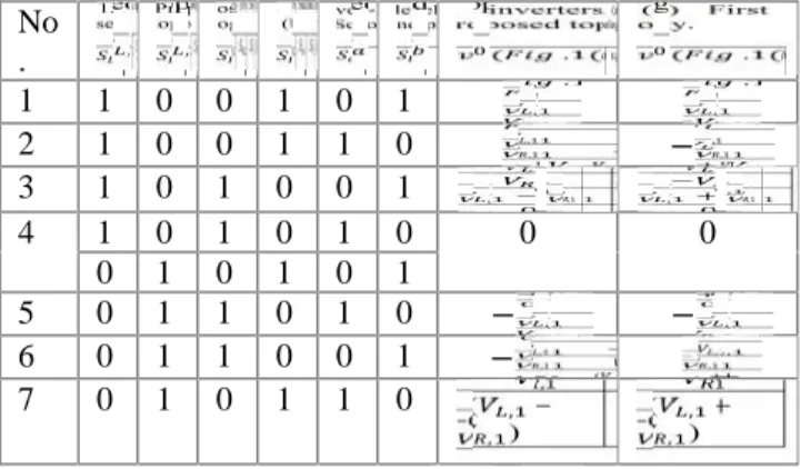
In Fig. 1, two new topologies are proposed for a seven-level inverter [19]. As appeared in Fig. 1, the proposed topologies are gotten by including two unidirectional power switches and one dc voltage source to the H-connect inverter structure. At the end of the day, the proposed inverters are included six unidirectional power switches ( , , , , , , , ,
, )and two dc voltage sources( , , ). In
this paper, these topologies are called developed H-bridge. As shown in Fig. 1, the simultaneous turn-on of
, , ( , , )
Fig. 1. Proposed seven-level inverters. (a) First proposed topology. (b) Second proposed topology.
No
. , , , ,
( .1( )) ( .1( ))
1 1 0 0 1 0 1 , ,
2 1 0 0 1 1 0 , − , 3 1 0 1 0 0 1 , − , , + ,
4 1 0 1 0 1 0 0 0
0 1 0 1 0 1
5 0 1 1 0 1 0 − , − , 6 0 1 1 0 0 1 − , , 7 0 1 0 1 1 0 -( , −
, )
-( , +
, )
causes the voltage sources to short-circuit. Therefore, the simultaneous turn-on of the mentioned switches must be avoided. In addition, and should not turn on, simultaneously. The distinction in the topologies delineated in Fig. 1 is in the association of the dc voltage sources extremity. Table I demonstrates the yield voltages of the proposed inverters for various conditions of the switches. In this table, 1 and 0 show the ON-and OFF-conditions of the switches, individually. As it is evident from Table I, if the estimations of the dc voltage sources are equivalent, the quantity of voltage levels abatements to three. Along these lines, the estimations of dc voltage sources ought to be distinctive to create more voltage levels without expanding the quantity of switches and dc voltage sources. Considering Table I, to produce all voltage
levels (odd and even) in the proposed topology appeared in Fig. 1(a), the extents of〖 V〗_(L,1) and V_(R,1) ought to be viewed as 3pu and 1pu, separately. Thus, for the topology appeared in Fig. 1(a), the extents of V_(L,1) and V_(R,1) ought to be viewed as 2pu and 1pu, individually. Considering the previously mentioned clarifications, the aggregate cost of the proposed topology in Fig. 1(b) is low since dc voltage sources with low sizes are required. By building up the seven-level inverter appeared in Fig. 1(b), the 31-level inverter appeared in Fig. 2 can be proposed. This topology comprises of ten unidirectional power switches and four dc voltage sources. As per Fig. 2, if the power switches of (S_(L,1),S_(L,2)), (S_(L,3),S_(L,4)), (S_(R,1),S_(R,2)), and (S_(R,3),S_(R,4)) turn on all the while, the dc voltage sources ofV_(L,1),V_(L,2),V_(R,1), and V_(R,2) will be shortcircuited, individually. Consequently, the concurrent turn-on of these switches ought to be kept away from. In addition, and should not turn on simultaneously. It is important to note that the 127-level topology can be provided through the structure presented in Fig. 1(a), where the only difference will be in the polarity of the applied dc voltage sources. By developing the proposed 49th level inverter, a 49th -level inverter can be proposed as shown in Fig. 3. This topology
Fig. 3. Proposed 49-level inverter.
consists of 14 unidirectional power switches and 6 dc voltage sources. Similarly, by developing the proposed basic topology, a general topology, as shown in Fig. 4, can be proposed. The general topology consists of2 dc voltage sources ( is the number of the dc voltage sources on each leg) and 4 + 2 unidirectional power switches. In the proposed general topology, the number of output voltage levels( ), number of switches( ), number of dc voltage sources( ), and the maximum magnitude of the generated voltage( , ) are calculated as follows, respectively:
= 2 − 1
--- (1)
= 4 + 2
--- (2)
= 2
--- (3)
, = , + ,
--- (4) The other important parameters of the total cost of a multilevel inverter for evaluation are the variety of the values of dc voltage sources and the value of the blocking voltage of the switches. As the variety of dc voltage sources and the value of the blocking voltage of the switches are low, the inverter’s totalcost decreases [20]. The number of variety of the values of dc voltage sources is given by
= 2
--- (5) The following pattern is utilized to calculate the maximum magnitude of the blocking voltage of the power switches. As shown in Fig. 1(b), the blocking voltage of , and , are calculated as follows:
, = , = ,
--- (6) Where , and , indicate the maximum blocking voltages of , and , , respectively. The blocking voltage of , and , are as follows:
, = , = ,
--- (7) Where , and , indicate the maximum blocking voltages of , and , , respectively. Therefore, the maximum blocking voltage of all switches in the proposed seven-level inverter( , )is calculated as follows:
, = , + , + , + , + +
= 4( , + , )
--- (8)
Considering Fig. 2, the maximum blocking voltage of the switches is as follows:
, = , = ,
--- (9)
, = , = , − ,
--- (10)
, = , = ,
--- (11)
, = , = , − ,
---(12)
= = , + ,
--- (13) Therefore, the maximum blocking voltage of all switches of the proposed 31-level inverter( , )is as follows:
, = , + , + , + , + , + ,
+ , + , + +
= 4( , + , )
--- (14) Similarly, the maximum blocking voltage of all switches of the 49-level inverter is calculated as follows:
, = 4( , + , )
--- (15) Finally, the maximum blocking voltage of all the switches of the general topology , is calculated as follows:
, = 4( , + , )
--- (16)
III. PROPOSED ALGORITHM TO DETERMINE THE MAGNITUDES OF DC VOLTAGE SOURCES In this paper, the following algorithm is applied to determine the magnitude of dc voltage sources. It is important to note that all voltage levels (even and odd) can be generated.
A. Proposed 49-Level Inverter
The magnitudes of the dc voltage sources of the proposed 127-level inverter are calculated as follows:
, =
--- (17)
, = 2
--- (18)
, = 5
--- (19)
, = 10
--- (20)
, = 25
--- (21)
, = 50
By using this algorithm, the inverter can generate all negative and positive voltage levels from 0 to 63 with steps of
D. Proposed General Multilevel Inverter
The magnitudes of the dc voltage sources of the proposed general multilevel inverter can be obtained as follows:
= 5 = 1,2,3, … . ,
--- (23)
= 2 × 5 = 1,2,3, … . ,
--- (24) Considering (4) and (16), the values of
, and , of the proposed general multilevel
inverter are as follows, respectively:
, = , + , = 3 × 5
--- (25)
, = 4 , + , = 12(5 )
--- (26)
IV. CALCULATION OF LOSSES
Mainly, two kinds of losses (i.e., conduction and switching losses) are associated with the switches. Since the switches include IGBTs and diodes, the conduction losses of an IGBT( , ( ))and a diode
( , ( )) are calculated as follows, respectively [7],
[22]:
, ( ) = + ( ) ( )
--- (27)
, ( ) = + ( ) ( )
--- (28) Where and are the forward voltage drops of the IGBT and diode, respectively. and are the equivalent resistances of the IGBT and diode, respectively, and is a constant related to the specification of the IGBT. Considering that at instant , there are transistors and diodes in the current path, the average value of the conduction power loss( )of the multilevel inverter can be written as follows:
=12 [ ( ) , ( ) + ( ) , ( )]
--- (29) The switching losses are calculated based on the energy loss calculation. The switching losses occur during the turn-off and turn-on periods. For simplicity, the linear variations of the voltage and current of the switches in the switching period are considered. Based on this assumption, the following relations can be written [7], [22]:
, = ( ) ( ) =16 ,
--- (28)
, = ( ) ( ) =16 , ′
--- (29) Where , and , are the turn-off and turn-on losses of the switch , respectively. and are the turn-off and turn-on times of the switch, respectively, is the current through the switch before turning off, ′is the current through the switch after
turning on, and , is the OFF-state voltage on the switch. The switching power loss ( ) is equal to the sum of all turn-on and turn-off energy losses in a fundamental cycle of the output voltage. This can be written as follows [7], [22]:
= , + ,
, ,
--- (30) Where is the fundamental frequency and , and
, are the numbers of turn-on and turn-off of the
switch during a fundamental cycle. Also, , is the energy loss of the switch during the ℎ turn-on and
, is the energy loss of the switch during the ℎ
turn-off. The total loss( )of the multilevel converter is the sum of the conduction and switching losses as follows:
= +
--- (31) Finally, the efficiency ( )of the inverter is calculated as follows:
= = +
--- (32) Where and denote the output and input powers of the inverter.
V. COMPARING THE PROPOSED GENERAL TOPOLOGY WITH THE CONVENTIONAL
TOPOLOGIES
and the conventional binary asymmetric cascaded multilevel inverter is shown by . Three other algorithms have been presented for this topology in [1], [17], and [18], which are indicated by – , respectively. Moreover, another topology with three different algorithms for determining the value of dc voltage sources has been introduced in [15], which are shown by – in this comparison. In [9]–[12], four different structures for the cascaded multilevel inverter have been presented, and in this paper, they are indicated by – and – . It is important to note that the power switches in the aforementioned topologies are unidirectional. In addition, other topologies based on bidirectional switches have been presented in [13] and [14]. In [14], three different algorithms have been recommended, which are denoted as – , and the presented topology in [13] is indicated by in this comparison. Fig. 5 shows all of the aforementioned structures. Fig. 6 compares the number of IGBTs of the proposed general topology with the aforementioned cascaded multilevel inverters. It is obvious that the proposed inverter requires a lesser number of IGBTs in comparison with the other mentioned topologies to generate particular levels. Fig. 7 compares the number of dc voltage sources of the proposed inverter with the aforementioned cascaded multilevel inverter. As shown in Fig. 7, the proposed inverter has better performance in comparison with the other presented topologies except the topology presented in . However, the magnitude of the dc voltage sources in is a little more than that of the proposed topology.
Fig. 8 compares the variety of magnitudes of the dc voltage sources of the proposed inverter with that of the aforementioned cascaded multilevel inverter. Obviously, the proposed inverter uses a wider variety of magnitudes of the dc voltage sources in comparison with those of all the aforementioned topologies. This feature is the most important disadvantage of the proposed topology because the variety of the values of dc voltage sources is as one of the remarkable factors in determining the cost of the inverter. However, this feature in the proposed topology is similar to the presented topologies of
and . Fig. 9 compares the magnitude of the blocking voltage of the switches of the proposed inverter with that of the aforementioned cascaded multilevel inverter. This figure shows the reduction of the magnitude of the blocking voltage of the proposed inverter in comparison with those of all the aforementioned multilevel inverters.
VI. SIMULATION RESULTS
In order to verify the correct performance of the proposed multilevel inverter in generating all output voltage levels (even and odd), a 49-level inverter based on the topology shown in Fig. 2 has been used for the simulation. Table II shows the switching states of the 49-level inverter.
Fig. 11 49 level voltage and current
The simulation is done by using MATLAB software, and the practical prototype is made in the experimental environment. Fig. 10 shows the experimental setup. It is important to note that the IGBTs used in the prototype are HGTP10N40CID (with an internal anti-parallel diode) with the voltage and current ranges of 400 V and 10 A, respectively. The 89C52 microcontroller by ATMEL Company has been used to generate all switching patterns. In all processes of the simulation and experiment, the load is assumed as R–L with R=
45ΩandL=55mH. Moreover, the magnitude ofVL,1 is
harmonic spectrum of the output voltage and current, respectively. The figure shows that the magnitudes of harmonics of both voltage and current waveforms are low. However, the harmonics of the current waveform are lower than the voltage
(a)Harmonic spectrum of output voltage of 31 level
inverter
(b)
Fig. 12. Harmonic spectrum of (a) output voltage of 49 level inverter
considered nonlinear. In the test condition, the measured input and output powers are about 1203 and 1112 W, respectively. Therefore, the efficiency is about 92.4%. Based on the loss calculations given before, the power loss is about 86 W. Therefore, the calculated loss has a good accordance with the measured efficiency. As mentioned before, the power switches in the proposed topology are unidirectional from the voltage viewpoint.
In order to prove this issue, the voltages on the switches of a single leg of the inverter
( . . , , , , , , , , , ) are shown in Fig. 13.
As can be seen, the maximum blocking voltage by switches , , , , , , , , are equal to 15, 15, 60, 60, and 225 V, respectively. Obviously, the voltage values are zero or equal to the positive ones, which is well in accordance to the unidirectional feature of the switches from the voltage view point. Considering the magnitude of the blocking voltage of the switches, the relations associated to the maximum voltage drop of the switches are well confirmed. Fig. 14 shows the experimental results of the implemented inverter. It is important to note that there is a good agreement between the experimental and simulation results.
VII. CONCLUSION
In this paper, two basic topologies have been proposed for multilevel inverters to generate seven voltage levels at the output. The basic topologies can be developed to any number of levels at the output where the 49-level and general topologies are consequently presented. In addition, a new algorithm to determine the magnitude of the dc voltage sources has been proposed. The proposed general topology was compared with the different kinds of presented topologies in literature from different points of view. According to the comparison results, the proposed topology requires a lesser number of IGBTs, power diodes, driver circuits, and dc voltage sources. Moreover, the magnitude of the blocking voltage of the switches is lower
Fig. 13. Voltages of switches (a) SL,1 , (b) SL,2
voltage sources in comparison with the others. The performance accuracy of the proposed topology was verified through the MATLAB simulation and the experimental results of a 49-level inverter.
REFERENCES
[1] Ebrahim Babaei, Member, IEEE, Somayeh Alilu, and Sara Laali, Student Member, IEEE” A New General Topology for Cascaded Multilevel Inverters With Reduced Number of Components Based on Developed H-Bridge” IEEE TRANSACTIONS ON INDUSTRIAL ELECTRONICS, VOL. 61, NO. 8, AUGUST 2014
[2] E. Babaei and S. H. Hosseini, “Charge balance
control methods for asymmetrical cascade multilevel converters,” inProc. ICEMS, Seoul, Korea, 2007, pp. 74–79.
[3] K. Wang, Y. Li, Z. Zheng, and L. Xu, “Voltage
balancing and fluctuationsuppression methods of floating capacitors in a new modular multilevel
converter,”IEEE Trans. Ind. Electron., vol. 60, no. 5,
pp. 1943–1954, May 2013.
[4] J. Ebrahimi, E. Babaei, and G. B. Gharehpetian, “A
new topology of cascaded multilevel converters with reduced number of components for high-voltage
applications,”IEEE Trans. Power Electron., vol. 26, no.
11, pp. 3109–3118, Nov. 2011.
[5] M. Manjrekar and T. A. Lipo, “A hybrid multilevel
inverter topology fordrive application,” inProc. APEC,
1998, pp. 523–529.
[6] M. Narimani and G. Moschopoulos, “A novel
single-stage multilevel type full-bridge converter,”IEEE
Trans. Ind. Electron., vol. 60, no. 1, pp. 31– 42, Jan. 2013.
[7] N. Abd Rahim, M. F. Mohamad Elias, and W. P.
Hew, “Transistor-clamped H-bridge based cascaded
multilevel inverter with new method of capacitor
voltage balancing,”IEEE Trans. Ind. Electron., vol. 60,
no. 8, pp. 2943–2956, Aug. 2013.
[8] S. R. Pulikanti, G. Konstantinou, and V. G.
Agelidis, “Hybrid seven-level cascaded active
neutral-point-clamped-based multilevel converter under
SHE-PWM,”IEEE Trans. Ind. Electron.,vol. 60, no. 11, pp.
4794–4804, Nov. 2013.
[9] Y. Hinago and H. Koizumi, “A single-phase
multilevel inverter using switched series/parallel dc voltage sources,”IEEE Trans. Ind. Electron., vol. 57, no. 8, pp. 2643–2650, Aug. 2010.
[10] G. Waltrich and I. Barbi, “Three-phase cascaded
multilevel inverter using power cells with two inverter legs in series,”IEEE Trans. Ind. Appl., vol. 57, no. 8, pp. 2605–2612, Aug. 2010.
[11] W. K. Choi and F. S. Kang, “H-bridge based
multilevel inverter using PWM switching function,”
inProc. INTELEC, 2009, pp. 1–5.
[12] E. Babaei, M. Farhadi Kangarlu, and F. Najaty
Mazgar, “Symmetric and asymmetric multilevel
inverter topologies with reduced switching
devices,”Elect. Power Syst. Res., vol. 86, pp. 122–130,
May 2012.
[13] J. Ebrahimi, E. Babaei, and G. B. Gharehpetian,
“A new multilevel converter topology with reduced
number of power electronic components,”IEEE Trans. Ind. Electron., vol. 59, no. 2, pp. 655–667, Feb. 2012. [14] E. Babaei, S. H. Hosseini, G. B. Gharehpetian, M. Tarafdar Haque, and M. Sabahi, “Reduction of DC
voltage sources and switches in asymmetrical multilevel converters using a novel topology,”Elect.
Power Syst. Res., vol. 77, no. 8, pp. 1073–1085, Jun. 2007.
[15] E. Babaei and S. H. Hosseini, “New cascaded
multilevel inverter topology with minimum number of
switches,”Energy Convers. Manage., vol. 50, no. 11,
pp. 2761–2767, Nov. 2009.
[16] S. Mekhilef and M. N. Kadir,“Voltage control of
three-stage hybrid multilevel inverter using vector transformation,”IEEE Trans. Power Electron., vol. 25, no. 10, pp. 2599–2606, Oct. 2010.
[17] A. Rufer, M. Veenstra, and K. Gopakumar,
“Asymmetric multilevel converter for high resolution
voltage phasor generation,” presented at theProc. EPE, Lausanne, Switzerland, 1999.
[18] S. Laali, K. Abbaszades, and H. Lesani, “A new
algorithm to determine the magnitudes of dc voltage sources in asymmetrical cascaded multilevel converters capable of using charge balance control methods,”